EP0455322B1 - Halbleiteranordnung - Google Patents
Halbleiteranordnung Download PDFInfo
- Publication number
- EP0455322B1 EP0455322B1 EP91301366A EP91301366A EP0455322B1 EP 0455322 B1 EP0455322 B1 EP 0455322B1 EP 91301366 A EP91301366 A EP 91301366A EP 91301366 A EP91301366 A EP 91301366A EP 0455322 B1 EP0455322 B1 EP 0455322B1
- Authority
- EP
- European Patent Office
- Prior art keywords
- main
- terminal
- support plate
- auxiliary
- electrode
- Prior art date
- Legal status (The legal status is an assumption and is not a legal conclusion. Google has not performed a legal analysis and makes no representation as to the accuracy of the status listed.)
- Expired - Lifetime
Links
Images


Classifications
-
- H—ELECTRICITY
- H02—GENERATION; CONVERSION OR DISTRIBUTION OF ELECTRIC POWER
- H02M—APPARATUS FOR CONVERSION BETWEEN AC AND AC, BETWEEN AC AND DC, OR BETWEEN DC AND DC, AND FOR USE WITH MAINS OR SIMILAR POWER SUPPLY SYSTEMS; CONVERSION OF DC OR AC INPUT POWER INTO SURGE OUTPUT POWER; CONTROL OR REGULATION THEREOF
- H02M7/00—Conversion of AC power input into DC power output; Conversion of DC power input into AC power output
- H02M7/003—Constructional details, e.g. physical layout, assembly, wiring or busbar connections
-
- H—ELECTRICITY
- H10—SEMICONDUCTOR DEVICES; ELECTRIC SOLID-STATE DEVICES NOT OTHERWISE PROVIDED FOR
- H10W—GENERIC PACKAGES, INTERCONNECTIONS, CONNECTORS OR OTHER CONSTRUCTIONAL DETAILS OF DEVICES COVERED BY CLASS H10
- H10W44/00—Electrical arrangements for controlling or matching impedance
- H10W44/501—Inductive arrangements
-
- H—ELECTRICITY
- H10—SEMICONDUCTOR DEVICES; ELECTRIC SOLID-STATE DEVICES NOT OTHERWISE PROVIDED FOR
- H10W—GENERIC PACKAGES, INTERCONNECTIONS, CONNECTORS OR OTHER CONSTRUCTIONAL DETAILS OF DEVICES COVERED BY CLASS H10
- H10W70/00—Package substrates; Interposers; Redistribution layers [RDL]
- H10W70/40—Leadframes
- H10W70/481—Leadframes for devices being provided for in groups H10D8/00 - H10D48/00
-
- H—ELECTRICITY
- H10—SEMICONDUCTOR DEVICES; ELECTRIC SOLID-STATE DEVICES NOT OTHERWISE PROVIDED FOR
- H10W—GENERIC PACKAGES, INTERCONNECTIONS, CONNECTORS OR OTHER CONSTRUCTIONAL DETAILS OF DEVICES COVERED BY CLASS H10
- H10W90/00—Package configurations
-
- H—ELECTRICITY
- H10—SEMICONDUCTOR DEVICES; ELECTRIC SOLID-STATE DEVICES NOT OTHERWISE PROVIDED FOR
- H10W—GENERIC PACKAGES, INTERCONNECTIONS, CONNECTORS OR OTHER CONSTRUCTIONAL DETAILS OF DEVICES COVERED BY CLASS H10
- H10W72/00—Interconnections or connectors in packages
- H10W72/071—Connecting or disconnecting
- H10W72/075—Connecting or disconnecting of bond wires
- H10W72/07551—Connecting or disconnecting of bond wires characterised by changes in properties of the bond wires during the connecting
- H10W72/07554—Connecting or disconnecting of bond wires characterised by changes in properties of the bond wires during the connecting changes in dispositions
-
- H—ELECTRICITY
- H10—SEMICONDUCTOR DEVICES; ELECTRIC SOLID-STATE DEVICES NOT OTHERWISE PROVIDED FOR
- H10W—GENERIC PACKAGES, INTERCONNECTIONS, CONNECTORS OR OTHER CONSTRUCTIONAL DETAILS OF DEVICES COVERED BY CLASS H10
- H10W72/00—Interconnections or connectors in packages
- H10W72/50—Bond wires
- H10W72/541—Dispositions of bond wires
- H10W72/5445—Dispositions of bond wires being orthogonal to a side surface of the chip, e.g. parallel arrangements
-
- H—ELECTRICITY
- H10—SEMICONDUCTOR DEVICES; ELECTRIC SOLID-STATE DEVICES NOT OTHERWISE PROVIDED FOR
- H10W—GENERIC PACKAGES, INTERCONNECTIONS, CONNECTORS OR OTHER CONSTRUCTIONAL DETAILS OF DEVICES COVERED BY CLASS H10
- H10W72/00—Interconnections or connectors in packages
- H10W72/50—Bond wires
- H10W72/541—Dispositions of bond wires
- H10W72/547—Dispositions of multiple bond wires
- H10W72/5473—Dispositions of multiple bond wires multiple bond wires connected to a common bond pad
-
- H—ELECTRICITY
- H10—SEMICONDUCTOR DEVICES; ELECTRIC SOLID-STATE DEVICES NOT OTHERWISE PROVIDED FOR
- H10W—GENERIC PACKAGES, INTERCONNECTIONS, CONNECTORS OR OTHER CONSTRUCTIONAL DETAILS OF DEVICES COVERED BY CLASS H10
- H10W72/00—Interconnections or connectors in packages
- H10W72/50—Bond wires
- H10W72/541—Dispositions of bond wires
- H10W72/547—Dispositions of multiple bond wires
- H10W72/5475—Dispositions of multiple bond wires multiple bond wires connected to common bond pads at both ends of the wires
-
- H—ELECTRICITY
- H10—SEMICONDUCTOR DEVICES; ELECTRIC SOLID-STATE DEVICES NOT OTHERWISE PROVIDED FOR
- H10W—GENERIC PACKAGES, INTERCONNECTIONS, CONNECTORS OR OTHER CONSTRUCTIONAL DETAILS OF DEVICES COVERED BY CLASS H10
- H10W72/00—Interconnections or connectors in packages
- H10W72/90—Bond pads, in general
- H10W72/921—Structures or relative sizes of bond pads
- H10W72/926—Multiple bond pads having different sizes
-
- H—ELECTRICITY
- H10—SEMICONDUCTOR DEVICES; ELECTRIC SOLID-STATE DEVICES NOT OTHERWISE PROVIDED FOR
- H10W—GENERIC PACKAGES, INTERCONNECTIONS, CONNECTORS OR OTHER CONSTRUCTIONAL DETAILS OF DEVICES COVERED BY CLASS H10
- H10W72/00—Interconnections or connectors in packages
- H10W72/90—Bond pads, in general
- H10W72/951—Materials of bond pads
-
- H—ELECTRICITY
- H10—SEMICONDUCTOR DEVICES; ELECTRIC SOLID-STATE DEVICES NOT OTHERWISE PROVIDED FOR
- H10W—GENERIC PACKAGES, INTERCONNECTIONS, CONNECTORS OR OTHER CONSTRUCTIONAL DETAILS OF DEVICES COVERED BY CLASS H10
- H10W90/00—Package configurations
- H10W90/701—Package configurations characterised by the relative positions of pads or connectors relative to package parts
- H10W90/751—Package configurations characterised by the relative positions of pads or connectors relative to package parts of bond wires
- H10W90/754—Package configurations characterised by the relative positions of pads or connectors relative to package parts of bond wires between a chip and a stacked insulating package substrate, interposer or RDL
Definitions
- the present invention relates to a semiconductor device that includes switching elements to control a current flowing between a pair of electrodes by means of signals given between an auxiliary electrode of the device and one of the main electrodes.
- switching elements include power transistors, and power MOSFET or insulation gate bipolar transistors (IGBT).
- DE-OS-37 34 067 discloses a semiconductor package wherein wire connection between the base and one of the main terminals and auxiliary terminals are made by attaching wires to the upstanding parts of the terminal strips.
- the upstanding parts are straight sections, and the connecting wires are intertwined.
- each electrode is conventionally connected to a lead-out terminal via a conductor plate that is insulated and fixed on the same support plate as the semiconductor piece.
- the electrode and the conductor plate are connected by an ordinary lead wire, and the conductor plate and the draw-out terminal are connected either by linking the draw-out terminal directly to the conductor plate or by means of a lead wire.
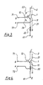
- Figures 2A, 2B and 2C show a prior art example of an IGBT semiconductor piece 1 fixed to a metal support plate 2 by means of a collector electrode beneath the semiconductor piece.
- a first conductor strip 41 is fixed via an insulating plate 3, and a second conductor strip 42 is fixed via a further insulating plate (not shown).
- An emitter electrode 11 on top of the semiconductor piece 1 is connected to the first conductor strip 41, and gate electrode 12 is connected to the second conductor strip 42, by lead wires 51 and 52 respectively.
- One end of the first conductor strip 41 is raised to form a main emitter terminal 6.
- auxiliary terminals 71 and 72 are fixed to the support plate 2 by means of an insulating plate 31.
- the auxiliary terminal 71 is connected to the second conductor strip 42 by a lead wire 53, thereby forming a gate terminal, and the auxiliary terminal 72 is connected to the first conductor strip 41 by a lead wire 54, thereby forming an auxiliary emitter terminal.
- FIG. 3 shows a circuit diagram of the prior art semiconductor device shown in Figures 2A, 2B and 2C.
- the same numerals are given to corresponding parts in Figures 2A, 2B, 2C and Figure 3.
- a resistance is connected in series to the gate terminal 71, and a voltage is applied between the gate electrode 12 and the emitter electrode 11 of the element 1 so slowly that it is determined by a time constant defined by the parasitic capacities 23 and 24 of the resistance and the element.
- This arrangement prevents the collector current from changing excessively upon start-up and shutdown.
- the delay time before the voltage reaches across the gate is too long, and the emitter voltage required for. the collector current 21 to start flowing into the element 1 is too great.
- the delay time across the gate and emitter causes the voltage to drop too much upon shutdown.
- the objective of the present invention is to provide a semiconductor device that prevents damage to elements caused by the surge voltages that are caused by the internal wiring board upon start-up or shutdown in the case where a switching element that has a fast turn-on/turn-off response speed is included. At the same time, this invention circumvents the excessive delay time at start-up or shutdown.
- a semiconductor device mounted on a planar metal support plate comprising;
- the wire controls the main current by applying a voltage across the first and second auxiliary terminals.
- the operation of the device will now be described. While the main current of the semiconductor flows in the wires connecting the main electrode to the main terminal, the circuit from the main electrode to the second auxiliary terminal also goes through most of the connecting wires. Therefore, the counter electromotive voltage generated by the main current and the inductance of the wiring to the main electrode is also applied between the first and second auxiliary terminals, thereby slowly increasing and decreasing the control voltage applied between the first and second auxiliary terminals. Thus, the surge voltage generated by a change in the main current, and the connecting wiring inductance, is suppressed.
- Figures 1A, 1B and 1C show a conventional IGBT arrangement, with the same reference numbers given to parts common to Figures 1A, 1B, 1C and Figures 2A, 2B, 2C.
- the emitter electrode 11 on top of the IGBT semiconductor piece 1 fixed on the metal support plate 2 by the collector electrode is connected to the first conductor strip 41 by the lead wire 51, and the gate electrode 12 is connected to the second conductor strip 42 by the lead wire 52, similar to the arrangement seen in Figures 2A, 2B and 2C.
- the terminal 71 rising from the support plate 2 and mounted on an insulating plate 31, and the auxiliary emitter terminal 72 are connected respectively to the conductor strips 41 and 42 by the lead wires 53 and 54.
- the upstanding part of the main emitter terminal 6 is located at the end of the first conductor strip 41 proximate to the auxiliary terminal 72, and provides the location for the connection point with the lead wire 54.
- connection point of the auxiliary emitter terminal 72 with the IGBT element 1 is placed in a position opposite to the element of the wiring inductance 22 in the lead wire 51 and the first conductor strip 41.
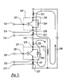
- Figure 5 shows a circuit diagram of one phase of a three-phase inverter circuit.
- IGBT elements 120 and 121 when IGBT elements 120 and 121 are housed in a container, inductances 122 to 125 comprising package components are inserted equivalently.
- the electrodes for each of the IGBT elements 120 and 121 are connected to each part constituting the semiconductor device at positions 126 to 131, while 132 and 133 refer to gate terminals, and 134 and 135 are auxiliary emitter terminals, being the conventional case in which they are remote from the vicinity of the semiconductor elements.
- Parts 136 and 137 are the lead-out positions according to the present invention.
- the counter electromotive voltage generated between the main current IC 138 and the inductance 123 will suppress the rise rate of the signal given between the gate and the emitter, whereby the rise of the main current IC is slowed down, and the surge voltage is less likely to generate. Additionally, when turned off, the reverse takes place, allowing the main current IC to reduce more slowly, and an overvoltage becomes less likely to happen.
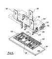
- Figure 6 is an exploded perspective view showing the package structure of a semiconductor device as shown by the equivalent circuit in Figure 5.
- FIG 6 the IGBT elements 120 and 121, and diode element 139 are fixed on the metal supporting plate 102.
- the current flows through the circuit pattern, and is led to an external circuit by the main terminals 126, 131, 141 held on a package component 103, and the auxiliary terminals 132, 133, 136, 137.
- Part 101 is a base to fix the metal supporting plate 102.
- Figures 7A to 7C are partially expanded drawings of the main emitter terminal 131 according to different embodiments of the invention. As shown in Figures 7A, 7B and 7C, an attempt is made to optimise the wiring inductance by means of changing the position of the connecting wire fixing to the auxiliary emitter terminal, and changing the shape of the main emitter terminal.
- FIG. 8 An semiconductor device utilising the inductance of a conduction pattern is shown in Figure 8.
- Parts 155 and 156 are IGBT elements, and 157 and 158 are diode elements.
- the main currents 181 and 182 flow through the conduction pattern formed on a circuit constituting component 152, and are led to the main terminal from positions 183 and 184.
- the take-out position of auxiliary terminals 185 and 186 shall be in the vicinity of the main terminais 183 and 184 that utilise inductance of the conduction pattern.
- the rapid rise or attenuation of the control voltage can be suppressed, and a generation of the excessive surge voltage can be prevented by the counter electromotive voltage generated from the main electrode connecting wiring when it is turned on or turned off, by placing the upstanding portion of the main terminal from the wiring connected to the main electrode of a switching element closer to the position of connection between the main terminal conductor and the auxiliary terminal. It was proved that an effect can be obtained to prevent the elements from an overvoltage destruction. Moreover, the time when the main current starts flowing when turned on, and the time when the main current starts to decrease when turned off, are not delayed.
Landscapes
- Engineering & Computer Science (AREA)
- Power Engineering (AREA)
- Power Conversion In General (AREA)
- Electronic Switches (AREA)
Claims (1)
- Halbleiteranordnung, die auf einer ebenen Metallhalteplatte (102) befestigt ist, mit:einer Halbleiterschaltungsanordnung (120), die eine auf einer erste Fläche angeordnete erste Hauptelektrode und eine zweite Hauptelektrode und Steuerelektrode, die auf ihrer zweiten Fläche angeordnet ist, aufweist, worin die Halbleiteranordnung an der Metallhalteplatte mittels ihrer ersten Hauptelektrode befestigt ist;einem Hauptanschluß (131) und ersten (132) und zweiten (136) Hilfsanschlüssen, die an der Halteplatte befestigt, aber von dieser elektrisch isoliert sind, wobei - jeder der Haupt- und Hilfsanschlüsse einen Leiterstreifen, der sich parallel zur Ebene der Halteplatte erstreckt, und einen hochstehenden Teil, der sich senkrecht zur Ebene der Halteplatte erstreckt, aufweist, die Steuerelektrode elektrisch durch eine Leitung mit dem Leiterstreifen des ersten Hilfsanschlusses (132) verbunden ist, der Leiterstreifen des Hauptanschlusses (131) mit der zweiten Hauptelektrode durch eine Leitung verbunden ist, worin das Anlegen einer Steuerspannung zwischen den ersten und zweiten Hilfsanschlüsse (132,136) gestattet, daß Strom zwischen den ersten und zweiten Hauptelektroden fließtund dadurch gekennzeichnet, daß der hochstehende Teil des Hauptanschlusses (131) erste und zweite Abschnitte aufweist, die sich senkrecht zur Ebene der Halteplatte (102) erstrecken, wobei der erste Abschnitt an dem Leiterstreifen angebracht ist, die ersten und zweiten Abschnitte durch zwei, vier, oder sechs rechtwinklige Winkelstücke verbunden sind, und dadurch, daß der Hauptanschluß (131) mit dem zweiten Hilfsanschluß (136) durch eine Leitung (154) verbunden ist, die an den zweiten Abschnitt des Hauptanschlusses (131) befestigt ist.
Applications Claiming Priority (4)
| Application Number | Priority Date | Filing Date | Title |
|---|---|---|---|
| JP4305590 | 1990-02-23 | ||
| JP43055/90 | 1990-02-23 | ||
| JP84254/90 | 1990-03-30 | ||
| JP2084254A JPH03263363A (ja) | 1990-02-23 | 1990-03-30 | 半導体装置 |
Publications (2)
| Publication Number | Publication Date |
|---|---|
| EP0455322A1 EP0455322A1 (de) | 1991-11-06 |
| EP0455322B1 true EP0455322B1 (de) | 1997-09-03 |
Family
ID=26382805
Family Applications (1)
| Application Number | Title | Priority Date | Filing Date |
|---|---|---|---|
| EP91301366A Expired - Lifetime EP0455322B1 (de) | 1990-02-23 | 1991-02-20 | Halbleiteranordnung |
Country Status (4)
| Country | Link |
|---|---|
| US (1) | US5164877A (de) |
| EP (1) | EP0455322B1 (de) |
| JP (1) | JPH03263363A (de) |
| DE (1) | DE69127494T2 (de) |
Families Citing this family (12)
| Publication number | Priority date | Publication date | Assignee | Title |
|---|---|---|---|---|
| JP2882143B2 (ja) * | 1991-12-10 | 1999-04-12 | 富士電機株式会社 | 半導体装置の内部配線構造 |
| JP3120575B2 (ja) * | 1992-06-29 | 2000-12-25 | 富士電機株式会社 | 半導体装置 |
| US5327318A (en) * | 1992-12-07 | 1994-07-05 | Texas Instruments Incorporated | Telecommunication equipment protector |
| JP2973799B2 (ja) * | 1993-04-23 | 1999-11-08 | 富士電機株式会社 | パワートランジスタモジュール |
| US5563447A (en) * | 1993-09-07 | 1996-10-08 | Delco Electronics Corp. | High power semiconductor switch module |
| US5978195A (en) * | 1998-02-23 | 1999-11-02 | Goder; Dimitry | Circuit protection arrangement |
| JP2003060157A (ja) * | 2001-08-08 | 2003-02-28 | Mitsubishi Electric Corp | パワーモジュール |
| DE10230156A1 (de) * | 2002-07-04 | 2004-01-22 | eupec Europäische Gesellschaft für Leistungshalbleiter mbH | Leistungshalbleitermodul und Schaltungsanordnung |
| JP4713963B2 (ja) * | 2005-07-07 | 2011-06-29 | 矢崎総業株式会社 | 過電流検出装置 |
| JP4701052B2 (ja) * | 2005-09-21 | 2011-06-15 | 矢崎総業株式会社 | 過電流検出装置 |
| CN104380463B (zh) | 2012-06-19 | 2017-05-10 | Abb 技术有限公司 | 用于将多个功率晶体管安装在其上的衬底和功率半导体模块 |
| JP6427589B2 (ja) | 2014-02-14 | 2018-11-21 | アーベーベー・シュバイツ・アーゲー | 2つの補助エミッタ導体経路を有する半導体モジュール |
Family Cites Families (6)
| Publication number | Priority date | Publication date | Assignee | Title |
|---|---|---|---|---|
| SU678585A1 (ru) * | 1978-02-10 | 1979-08-05 | Московский Ордена Трудового Красного Знамени Инженерно-Строительный Институт Им.В.В.Куйбышева | Устройство защиты инвертора с входным дросселем |
| JPS5892243A (ja) * | 1981-11-27 | 1983-06-01 | Mitsubishi Electric Corp | 電界効果トランジスタ用パツケ−ジ |
| JPS5984458A (ja) * | 1982-11-04 | 1984-05-16 | Mitsubishi Electric Corp | ゲ−トタ−ンオフサイリスタ組立体 |
| US4635158A (en) * | 1985-11-22 | 1987-01-06 | The United States Of America As Represented By The Secretary Of The Army | Filtering transient voltage suppression device assembly |
| JPS6393126A (ja) * | 1986-10-08 | 1988-04-23 | Fuji Electric Co Ltd | 半導体装置 |
| US4791521A (en) * | 1987-04-07 | 1988-12-13 | Western Digital Corporation | Method and apparatus for reducing transient noise by premagnetization of parasitic inductance |
-
1990
- 1990-03-30 JP JP2084254A patent/JPH03263363A/ja active Pending
-
1991
- 1991-02-20 DE DE69127494T patent/DE69127494T2/de not_active Expired - Fee Related
- 1991-02-20 EP EP91301366A patent/EP0455322B1/de not_active Expired - Lifetime
- 1991-02-22 US US07/659,995 patent/US5164877A/en not_active Expired - Lifetime
Also Published As
| Publication number | Publication date |
|---|---|
| US5164877A (en) | 1992-11-17 |
| DE69127494D1 (de) | 1997-10-09 |
| DE69127494T2 (de) | 1998-03-19 |
| JPH03263363A (ja) | 1991-11-22 |
| EP0455322A1 (de) | 1991-11-06 |
Similar Documents
| Publication | Publication Date | Title |
|---|---|---|
| JP2960375B2 (ja) | 電力モジュール | |
| EP0809292B1 (de) | Leistungstransistormodul | |
| EP0379346B1 (de) | Energieumwandlungseinheit und Modul für ihren Aufbau | |
| US6359331B1 (en) | High power switching module | |
| EP0455322B1 (de) | Halbleiteranordnung | |
| JP2004214452A (ja) | 電力用半導体モジュールおよび外部電極との結線方法 | |
| US4825279A (en) | Semiconductor device | |
| US6452261B1 (en) | Flat semiconductor device and power converter employing the same | |
| US20020024134A1 (en) | Semiconductor device | |
| EP0418891B1 (de) | Leistungshalbleiteranordnung mit Plastikumhüllung | |
| US6281569B1 (en) | Pressure-contact semiconductor device | |
| JP2005216876A (ja) | 電力用半導体モジュール | |
| EP0417747B1 (de) | Modultyp-Halbleiteranordnung von hoher Leistungskapazität | |
| US6795324B2 (en) | Power converter | |
| US5617293A (en) | Bridge module | |
| JP3787037B2 (ja) | 半導体モジュール | |
| JP3421544B2 (ja) | 半導体モジュール | |
| JP3156461B2 (ja) | スナバユニット | |
| EP0527033B1 (de) | Halbleitermodul | |
| JP2002238260A (ja) | 半導体装置 | |
| JP2002171768A (ja) | 電力変換装置 | |
| JPH03108749A (ja) | 電力変換装置用トランジスタモジュール | |
| US20020145188A1 (en) | Flat semiconductor device and power converter employing the same | |
| JPH07297695A (ja) | 半導体装置 | |
| JP2894402B2 (ja) | 半導体装置 |
Legal Events
| Date | Code | Title | Description |
|---|---|---|---|
| PUAI | Public reference made under article 153(3) epc to a published international application that has entered the european phase |
Free format text: ORIGINAL CODE: 0009012 |
|
| AK | Designated contracting states |
Kind code of ref document: A1 Designated state(s): DE FR GB |
|
| 17P | Request for examination filed |
Effective date: 19920212 |
|
| 17Q | First examination report despatched |
Effective date: 19940613 |
|
| GRAG | Despatch of communication of intention to grant |
Free format text: ORIGINAL CODE: EPIDOS AGRA |
|
| GRAH | Despatch of communication of intention to grant a patent |
Free format text: ORIGINAL CODE: EPIDOS IGRA |
|
| GRAH | Despatch of communication of intention to grant a patent |
Free format text: ORIGINAL CODE: EPIDOS IGRA |
|
| GRAA | (expected) grant |
Free format text: ORIGINAL CODE: 0009210 |
|
| AK | Designated contracting states |
Kind code of ref document: B1 Designated state(s): DE FR GB |
|
| REF | Corresponds to: |
Ref document number: 69127494 Country of ref document: DE Date of ref document: 19971009 |
|
| ET | Fr: translation filed | ||
| PLBE | No opposition filed within time limit |
Free format text: ORIGINAL CODE: 0009261 |
|
| STAA | Information on the status of an ep patent application or granted ep patent |
Free format text: STATUS: NO OPPOSITION FILED WITHIN TIME LIMIT |
|
| 26N | No opposition filed | ||
| PGFP | Annual fee paid to national office [announced via postgrant information from national office to epo] |
Ref country code: FR Payment date: 20010213 Year of fee payment: 11 |
|
| PGFP | Annual fee paid to national office [announced via postgrant information from national office to epo] |
Ref country code: GB Payment date: 20010214 Year of fee payment: 11 |
|
| REG | Reference to a national code |
Ref country code: GB Ref legal event code: IF02 |
|
| PG25 | Lapsed in a contracting state [announced via postgrant information from national office to epo] |
Ref country code: GB Free format text: LAPSE BECAUSE OF NON-PAYMENT OF DUE FEES Effective date: 20020220 |
|
| GBPC | Gb: european patent ceased through non-payment of renewal fee |
Effective date: 20020220 |
|
| PG25 | Lapsed in a contracting state [announced via postgrant information from national office to epo] |
Ref country code: FR Free format text: LAPSE BECAUSE OF NON-PAYMENT OF DUE FEES Effective date: 20021031 |
|
| REG | Reference to a national code |
Ref country code: FR Ref legal event code: ST |
|
| PGFP | Annual fee paid to national office [announced via postgrant information from national office to epo] |
Ref country code: DE Payment date: 20080214 Year of fee payment: 18 |
|
| PG25 | Lapsed in a contracting state [announced via postgrant information from national office to epo] |
Ref country code: DE Free format text: LAPSE BECAUSE OF NON-PAYMENT OF DUE FEES Effective date: 20090901 |