EP0455832A1 - Electrode ohmique a base de nitrure de bore cubique de type n et procede de production d'une telle electrode - Google Patents
Electrode ohmique a base de nitrure de bore cubique de type n et procede de production d'une telle electrode Download PDFInfo
- Publication number
- EP0455832A1 EP0455832A1 EP90917695A EP90917695A EP0455832A1 EP 0455832 A1 EP0455832 A1 EP 0455832A1 EP 90917695 A EP90917695 A EP 90917695A EP 90917695 A EP90917695 A EP 90917695A EP 0455832 A1 EP0455832 A1 EP 0455832A1
- Authority
- EP
- European Patent Office
- Prior art keywords
- alloy
- thin
- ohmic electrode
- film
- cbn
- Prior art date
- Legal status (The legal status is an assumption and is not a legal conclusion. Google has not performed a legal analysis and makes no representation as to the accuracy of the status listed.)
- Withdrawn
Links
Images
Classifications
-
- H—ELECTRICITY
- H10—SEMICONDUCTOR DEVICES; ELECTRIC SOLID-STATE DEVICES NOT OTHERWISE PROVIDED FOR
- H10D—INORGANIC ELECTRIC SEMICONDUCTOR DEVICES
- H10D64/00—Electrodes of devices having potential barriers
- H10D64/01—Manufacture or treatment
- H10D64/011—Manufacture or treatment of electrodes ohmically coupled to a semiconductor
- H10D64/0116—Manufacture or treatment of electrodes ohmically coupled to a semiconductor to Group III-V semiconductors
-
- H—ELECTRICITY
- H10—SEMICONDUCTOR DEVICES; ELECTRIC SOLID-STATE DEVICES NOT OTHERWISE PROVIDED FOR
- H10D—INORGANIC ELECTRIC SEMICONDUCTOR DEVICES
- H10D62/00—Semiconductor bodies, or regions thereof, of devices having potential barriers
- H10D62/80—Semiconductor bodies, or regions thereof, of devices having potential barriers characterised by the materials
- H10D62/85—Semiconductor bodies, or regions thereof, of devices having potential barriers characterised by the materials being Group III-V materials, e.g. GaAs
-
- H—ELECTRICITY
- H10—SEMICONDUCTOR DEVICES; ELECTRIC SOLID-STATE DEVICES NOT OTHERWISE PROVIDED FOR
- H10D—INORGANIC ELECTRIC SEMICONDUCTOR DEVICES
- H10D64/00—Electrodes of devices having potential barriers
- H10D64/60—Electrodes characterised by their materials
- H10D64/62—Electrodes ohmically coupled to a semiconductor
Definitions
- the present invention relates to a process for producing an ohmic electrode for n-type cubic boron nitride.
- One object of the present invention is to provide an even n-type cBN electrode having good ohmic characteristics which are effectively utilized, e. g., for the preparation of a semiconductor device using a cBN crystal.
- the present invention relates to an ohmic electrode for n-type cBN, and also relates to a process for producing an ohmic electrode for n-type cBN, which comprises the following steps; providing at least one thin alloy film selected from Au-Si alloy, Au-Ge alloy and Au-Si-Ge alloy, the weight ratio of Si, Ge and Si plus Ge being 0.1 to 35 % by weight, on n-type cBN; providing a thin film of at least one metal selected from Ni, Cr, Mo and Pt on the thin alloy film; and subjecting the n-type cBN having the thin films thus provided to a heat treatment in an inert gas or in a vaccum at a temperature ranging from 350°C to 600 °C . Concerning the inert gas, N2, Ar and a mixture of Ar and N2 are preferable.
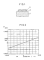
- FIG. 1 showing a schematic sectional view of the electrode produced by the process of the present invention, one embodiment of the article and the process for producing an ohmic electrode according to the present invention is explained.
- This invention provides the ohmic electrode for n-type cBN 1, on which the first thin film 2 of at least one alloy selected from Au-Si alloy, Au-Ge alloy and Au-Si-Ge alloy is coated, and the second thin film of at least one metal or alloy selected from Ni, Cr, Mo and Pt is coated.
- the process of the present invention may comprise the following steps: one, providing at least one thin film 2 of an alloy selected from Au-Si alloy, Au-Ge alloy and Au-Si-Ge alloy onto the surface of an n-type cBN crystal 1; two, providing at least one thin film 3 of a metal selected from Ni, Cr, Mo and Pt onto the thin film 2, and three, heat-treating the n-type cBN having the aforesaid thin film 2 and the thin film 3 at a temperature ranging from 350 °C to 600 °C in an inert gas atmosphere or in a vacuum.
- the wetting property of the Au-Si alloy, Au-Ge alloy and Au-Si-Ge alloy is improved to solve the aforesaid problem caused by poor wetting properties, and an ohmic electrode having the desired form can be obtained by means of a heat-treatment after vapor depositing a thin film of a metal selected from Ni, Cr, Mo and Pt or a thin alloy film thereby onto the thin Au-Si alloy, Au-Ge alloy and Au-Si-Ge alloy film.
- the heat treatment is generally conducted for from 5 to 60 minutes.
- the method for providing the thin alloy film and the thin film of Ni, Cr, Mo or Pt is not limited, and may be vapor deposition or sputtering.
- Ni, Cr, Mo and Pt are preferably used especially Ni and Cr are preferable from an economical point of view, and Ni is more preferably used in the present invention in view of a stability of the thin film.
- the content of Si, Ge, Si plus Ge in the Au-Si alloy, Au-Ge alloy and Au-Si-Ge alloy is from 0.1 % to 35 % by weight. If the content of Si, Ge, Si plus Ge is less than 0.1 % by weight, the electrode obtained does not show good ohmic characteristics, while if the content is over 35 % by weight, a thin alloy film having a sufficient junction strength with the cBN crystal is not obtained.
- the thickness of the aforementioned thin film of Ni, Cr, Mo and Pt with the ability to inhibit the aggregation of Au-Si alloy, Au-Ge alloy and Au-Si-Ge alloy film may generally be at least about 200 ⁇ , preferably from 200 to 2000 ⁇ .
- the aforementioned thin film of Ni, Cr, Mo and Pt are formed by itself or as an alloy film.
- the thickness of the thin alloy film of Au-Si alloy, Au-Ge alloy and Au-Si-Ge alloy is generally from 1000 ⁇ to 1 ⁇ m , preferably from 1000 to 3000 ⁇ .
- Vacuum deposition, sputtering and an ion plating method can be used for making a thin film of Au-Si alloy, Au-Ge alloy, Au-Si-Ge alloy, Ni, Cr, Mo and Pt.
- the ion plating method is preferably employed.
- the vapor deposition method is preferably employed in view of the production cost.
- an n-type cBN crystal consists of two layers can be used for n-type cBN crystals, but after the heat treatment the n-type cBN crystal has markedly better ohmic properties.
- a thin Au-Si alloy film containing 2.5 % of Si by weight, and having thickness of about 2000 ⁇ was vacuum vapor deposited on an n-type cBN crystal and then a thin Cr film having a thickness of about 500 ⁇ is further deposited thereon.
- the crystal having the coated film was heat treated for 10 minutes in an inert gas atmosphere at 480 °C .
- the electrode thus formed did not cause the phenomenon of aggregation such as an island and when current voltage characteristics were measured, good ohmic characteristics as shown in Fig. 2 were obtained.
- a flat n-type cBN electrode having good ohmic characteristics could be obtained and hence the present invention can be effectively utilized for the preparation of a semiconductor device using a cBN crystal.
Landscapes
- Electrodes Of Semiconductors (AREA)
Abstract
L'invention se rapporte à une électrode ohmique à base de nitrure de bore cubique de type N, qui se compose d'au moins deux films minces, la première couche étant constituée par au moins un alliage choisi dans le groupe composé des alliages Au-Si, Au-Ge et Au-Si-Ge et la seconde couche étant constituée par au moins un métal choisi dans le groupe composés des éléments Ni, Cr, Mo et Pt, ou par un alliage de ces éléments. L'invention se rapporte en outre à un procédé de production d'une électrode ohmique à base de nitrure de bore cubique de type N, qui consiste à former sur un nitrure de bore cubique de type N une première couche constituée par au moins un alliage choisi dans le groupe composé des alliages Au-Si, Au-Ge et Au-Si-Ge contenant 0,1 à 35 % en poids de Si et Ge, à former une seconde couche constituée par un métal choisi dans le groupe composé des éléments Ni, Cr, Mo et Pt ou par un alliage de ces éléments, puis à soumettre le produit ainsi formé à un traitement thermique dans une atmosphère inerte ou sous vide.
Applications Claiming Priority (2)
| Application Number | Priority Date | Filing Date | Title |
|---|---|---|---|
| JP308431/89 | 1989-11-28 | ||
| JP1308431A JPH03167877A (ja) | 1989-11-28 | 1989-11-28 | n型立方晶窒化硼素のオーム性電極及びその形成方法 |
Publications (2)
| Publication Number | Publication Date |
|---|---|
| EP0455832A1 true EP0455832A1 (fr) | 1991-11-13 |
| EP0455832A4 EP0455832A4 (en) | 1992-10-07 |
Family
ID=17980969
Family Applications (1)
| Application Number | Title | Priority Date | Filing Date |
|---|---|---|---|
| EP19900917695 Withdrawn EP0455832A4 (en) | 1989-11-28 | 1990-11-28 | Ohmic electrode of n-type cubic boron nitride and method of forming the same |
Country Status (5)
| Country | Link |
|---|---|
| US (1) | US5187560A (fr) |
| EP (1) | EP0455832A4 (fr) |
| JP (1) | JPH03167877A (fr) |
| WO (1) | WO1991008582A1 (fr) |
| ZA (1) | ZA909561B (fr) |
Cited By (1)
| Publication number | Priority date | Publication date | Assignee | Title |
|---|---|---|---|---|
| EP0458353A3 (en) * | 1990-05-24 | 1992-04-08 | Sumitomo Electric Industries, Ltd. | Ohmic contact electrodes for n-type semiconductor cubic boron nitride |
Families Citing this family (9)
| Publication number | Priority date | Publication date | Assignee | Title |
|---|---|---|---|---|
| JPH0697690B2 (ja) * | 1992-09-28 | 1994-11-30 | 科学技術庁無機材質研究所長 | オーム性電極を備えたcBN半導体装置とその製造方法 |
| JP2942452B2 (ja) * | 1993-10-21 | 1999-08-30 | 財団法人地球環境産業技術研究機構 | n型半導体立方晶窒化ホウ素のオ−ミック電極およびその形成方法 |
| US6143655A (en) | 1998-02-25 | 2000-11-07 | Micron Technology, Inc. | Methods and structures for silver interconnections in integrated circuits |
| US6121126A (en) | 1998-02-25 | 2000-09-19 | Micron Technologies, Inc. | Methods and structures for metal interconnections in integrated circuits |
| US5920121A (en) * | 1998-02-25 | 1999-07-06 | Micron Technology, Inc. | Methods and structures for gold interconnections in integrated circuits |
| US6492694B2 (en) | 1998-02-27 | 2002-12-10 | Micron Technology, Inc. | Highly conductive composite polysilicon gate for CMOS integrated circuits |
| US6815303B2 (en) * | 1998-04-29 | 2004-11-09 | Micron Technology, Inc. | Bipolar transistors with low-resistance emitter contacts |
| KR100461788B1 (ko) * | 2002-04-29 | 2004-12-14 | 학교법인 포항공과대학교 | 실리콘 게르마늄 반도체 기판에서의 저 저항 메탈 전극구조와 제조방법 |
| CN108400227B (zh) * | 2018-05-04 | 2023-08-15 | 佛山市国星半导体技术有限公司 | 一种倒装led芯片及其制作方法 |
Family Cites Families (12)
| Publication number | Priority date | Publication date | Assignee | Title |
|---|---|---|---|---|
| US3684930A (en) * | 1970-12-28 | 1972-08-15 | Gen Electric | Ohmic contact for group iii-v p-types semiconductors |
| US3753804A (en) * | 1971-08-31 | 1973-08-21 | Philips Corp | Method of manufacturing a semiconductor device |
| US3850688A (en) * | 1971-12-29 | 1974-11-26 | Gen Electric | Ohmic contact for p-type group iii-v semiconductors |
| US3965279A (en) * | 1974-09-03 | 1976-06-22 | Bell Telephone Laboratories, Incorporated | Ohmic contacts for group III-V n-type semiconductors |
| JPS5629381A (en) * | 1979-08-17 | 1981-03-24 | Toshiba Corp | Compound-semiconductor light emitting element containing garium and manufacture thereof |
| US4366186A (en) * | 1979-09-27 | 1982-12-28 | Bell Telephone Laboratories, Incorporated | Ohmic contact to p-type InP |
| JPS58112336A (ja) * | 1981-12-25 | 1983-07-04 | Mitsubishi Electric Corp | 化合物半導体装置の電極形成法 |
| EP0105324A4 (fr) * | 1982-04-12 | 1986-07-24 | Motorola Inc | CONTACT OHMIQUE POUR GaAs DE TYPE N. |
| US4831212A (en) * | 1986-05-09 | 1989-05-16 | Nissin Electric Company, Limited | Package for packing semiconductor devices and process for producing the same |
| US5006914A (en) * | 1988-12-02 | 1991-04-09 | Advanced Technology Materials, Inc. | Single crystal semiconductor substrate articles and semiconductor devices comprising same |
| JPH03137081A (ja) * | 1989-10-23 | 1991-06-11 | Sumitomo Electric Ind Ltd | p型cBNのオーム性電極形成方法 |
| JP3382484B2 (ja) * | 1996-12-27 | 2003-03-04 | 東芝テック株式会社 | 電気掃除機の吸込口体 |
-
1989
- 1989-11-28 JP JP1308431A patent/JPH03167877A/ja active Pending
-
1990
- 1990-11-28 WO PCT/JP1990/001537 patent/WO1991008582A1/fr not_active Ceased
- 1990-11-28 EP EP19900917695 patent/EP0455832A4/en not_active Withdrawn
- 1990-11-28 ZA ZA909561A patent/ZA909561B/xx unknown
- 1990-11-28 US US07/689,887 patent/US5187560A/en not_active Expired - Fee Related
Cited By (3)
| Publication number | Priority date | Publication date | Assignee | Title |
|---|---|---|---|---|
| EP0458353A3 (en) * | 1990-05-24 | 1992-04-08 | Sumitomo Electric Industries, Ltd. | Ohmic contact electrodes for n-type semiconductor cubic boron nitride |
| US5285109A (en) * | 1990-05-24 | 1994-02-08 | Sumitomo Electric Industries, Ltd. | Ohmic contact electrodes for n-type semiconductor cubic boron nitride |
| US5422500A (en) * | 1990-05-24 | 1995-06-06 | Sumitomo Electric Industries, Ltd. | Ohmic contact electrodes for N-type semiconductor cubic boron nitride |
Also Published As
| Publication number | Publication date |
|---|---|
| US5187560A (en) | 1993-02-16 |
| JPH03167877A (ja) | 1991-07-19 |
| ZA909561B (en) | 1992-04-29 |
| WO1991008582A1 (fr) | 1991-06-13 |
| EP0455832A4 (en) | 1992-10-07 |
Similar Documents
| Publication | Publication Date | Title |
|---|---|---|
| JPH03133176A (ja) | 炭化珪素半導体装置およびその製造方法 | |
| EP0455832A1 (fr) | Electrode ohmique a base de nitrure de bore cubique de type n et procede de production d'une telle electrode | |
| US4509066A (en) | Sputtered semiconducting films of catenated phosphorus material and devices formed therefrom | |
| EP0424857B1 (fr) | Procédé de fabrication d'une électrode ohmique pour nitrure de bore cubique de type P | |
| US4853346A (en) | Ohmic contacts for semiconductor devices and method for forming ohmic contacts | |
| US4035526A (en) | Evaporated solderable multilayer contact for silicon semiconductor | |
| US5240877A (en) | Process for manufacturing an ohmic electrode for n-type cubic boron nitride | |
| US5192994A (en) | Au-ge-ni ohmic contact for ga-al-as compound semiconductor | |
| JPH07122724A (ja) | n型半導体立方晶窒化ホウ素のオ−ミック電極およびその形成方法 | |
| JP3439597B2 (ja) | n型SiC用オーミック電極とその製造方法 | |
| Nadkarni et al. | Fabrication of high sensitivity thin-film indium antimonide magnetoresistors | |
| JPH0320007A (ja) | 磁性体薄膜の製造方法 | |
| US5387549A (en) | Process for fabricating ohmic contact | |
| Fane | The production of amorphous silicon without hydrogen | |
| JP2543073B2 (ja) | 超電導薄膜の製造方法 | |
| JPH0144518B2 (fr) | ||
| JP2514091B2 (ja) | 磁電変換素子 | |
| CA2260574A1 (fr) | Contact ohmique et processus de fabrication de ce genre de contact | |
| US5283233A (en) | Method for producing a superconductor layer of YBa2 Cu3 O7 on a sapphire substrate | |
| JPH05319984A (ja) | 金属エピタキシャル膜の製造方法 | |
| JP2821885B2 (ja) | 超伝導薄膜の形成方法 | |
| US5008215A (en) | Process for preparing high sensitivity semiconductive magnetoresistance element | |
| JPS6159656B2 (fr) | ||
| JPH01120715A (ja) | 酸化物超電導成形体 | |
| JPH09289341A (ja) | 薄膜形成方法および超電導素子形成方法 |
Legal Events
| Date | Code | Title | Description |
|---|---|---|---|
| PUAI | Public reference made under article 153(3) epc to a published international application that has entered the european phase |
Free format text: ORIGINAL CODE: 0009012 |
|
| 17P | Request for examination filed |
Effective date: 19910819 |
|
| AK | Designated contracting states |
Kind code of ref document: A1 Designated state(s): DE FR GB |
|
| A4 | Supplementary search report drawn up and despatched |
Effective date: 19920818 |
|
| AK | Designated contracting states |
Kind code of ref document: A4 Designated state(s): DE FR GB |
|
| 17Q | First examination report despatched |
Effective date: 19941028 |
|
| STAA | Information on the status of an ep patent application or granted ep patent |
Free format text: STATUS: THE APPLICATION IS DEEMED TO BE WITHDRAWN |
|
| 18D | Application deemed to be withdrawn |
Effective date: 19950509 |