EP0458321A2 - Procédé et dispositif pour fabriquer un écran à cristal liquide - Google Patents
Procédé et dispositif pour fabriquer un écran à cristal liquide Download PDFInfo
- Publication number
- EP0458321A2 EP0458321A2 EP91108329A EP91108329A EP0458321A2 EP 0458321 A2 EP0458321 A2 EP 0458321A2 EP 91108329 A EP91108329 A EP 91108329A EP 91108329 A EP91108329 A EP 91108329A EP 0458321 A2 EP0458321 A2 EP 0458321A2
- Authority
- EP
- European Patent Office
- Prior art keywords
- liquid crystal
- crystal panel
- temperature
- injection port
- transfer member
- Prior art date
- Legal status (The legal status is an assumption and is not a legal conclusion. Google has not performed a legal analysis and makes no representation as to the accuracy of the status listed.)
- Granted
Links
Images

Classifications
-
- G—PHYSICS
- G02—OPTICS
- G02F—OPTICAL DEVICES OR ARRANGEMENTS FOR THE CONTROL OF LIGHT BY MODIFICATION OF THE OPTICAL PROPERTIES OF THE MEDIA OF THE ELEMENTS INVOLVED THEREIN; NON-LINEAR OPTICS; FREQUENCY-CHANGING OF LIGHT; OPTICAL LOGIC ELEMENTS; OPTICAL ANALOGUE/DIGITAL CONVERTERS
- G02F1/00—Devices or arrangements for the control of the intensity, colour, phase, polarisation or direction of light arriving from an independent light source, e.g. switching, gating or modulating; Non-linear optics
- G02F1/01—Devices or arrangements for the control of the intensity, colour, phase, polarisation or direction of light arriving from an independent light source, e.g. switching, gating or modulating; Non-linear optics for the control of the intensity, phase, polarisation or colour
- G02F1/13—Devices or arrangements for the control of the intensity, colour, phase, polarisation or direction of light arriving from an independent light source, e.g. switching, gating or modulating; Non-linear optics for the control of the intensity, phase, polarisation or colour based on liquid crystals, e.g. single liquid crystal display cells
- G02F1/133—Constructional arrangements; Operation of liquid crystal cells; Circuit arrangements
-
- G—PHYSICS
- G02—OPTICS
- G02F—OPTICAL DEVICES OR ARRANGEMENTS FOR THE CONTROL OF LIGHT BY MODIFICATION OF THE OPTICAL PROPERTIES OF THE MEDIA OF THE ELEMENTS INVOLVED THEREIN; NON-LINEAR OPTICS; FREQUENCY-CHANGING OF LIGHT; OPTICAL LOGIC ELEMENTS; OPTICAL ANALOGUE/DIGITAL CONVERTERS
- G02F1/00—Devices or arrangements for the control of the intensity, colour, phase, polarisation or direction of light arriving from an independent light source, e.g. switching, gating or modulating; Non-linear optics
- G02F1/01—Devices or arrangements for the control of the intensity, colour, phase, polarisation or direction of light arriving from an independent light source, e.g. switching, gating or modulating; Non-linear optics for the control of the intensity, phase, polarisation or colour
- G02F1/13—Devices or arrangements for the control of the intensity, colour, phase, polarisation or direction of light arriving from an independent light source, e.g. switching, gating or modulating; Non-linear optics for the control of the intensity, phase, polarisation or colour based on liquid crystals, e.g. single liquid crystal display cells
- G02F1/133—Constructional arrangements; Operation of liquid crystal cells; Circuit arrangements
- G02F1/1333—Constructional arrangements; Manufacturing methods
- G02F1/1341—Filling or closing of cells
Definitions
- the present invention relates to a process and an apparatus for producing a liquid crystal panel, particularly a process and an apparatus for producing a liquid crystal panel by injecting a ferroelectric liquid crystal into a liquid crystal cell.
- An object of the present invention is to provide a process and an apparatus which are optimum for producing a liquid crystal panel by injection of a ferroelectric liquid crystal panel through an improvement of such a conventional method of injecting a liquid crystal material into a liquid crystal panel to reduce the loss of liquid crystal material and the load of the washing as a post-step.
- a process for producing a liquid crystal panel comprising the steps of: placing a blank liquid crystal panel having an injection port and a liquid crystal reservoir containing a liquid crystal within a vacuum environment, causing a transfer member moving between the liquid crystal reservoir and the liquid crystal panel to carry a portion of the liquid crystal in the liquid crystal reservoir, applying the liquid crystal carried on the transfer member to the injection port of the liquid crystal panel, and placing the injection port of the liquid crystal panel within an environment of atmospheric pressure.
- a process for producing a liquid crystal panel comprising: applying a liquid crystal contained in a liquid crystal reservoir to an injection port of a blank liquid crystal panel in a vacuum space and then restoring the pressure of the vacuum space to an atmospheric pressure to inject the liquid crystal into the liquid crystal panel; wherein a transfer member moving between the liquid crystal reservoir and the liquid crystal panel is used to carry the liquid crystal within the liquid crystal reservoir and then apply the liquid crystal to the injection port of the liquid crystal panel.
- an apparatus for producing a liquid crystal panel comprising: a vacuum chamber, and a liquid crystal panel having an injection port and a liquid crystal reservoir containing a liquid crystal disposed within the vacuum chamber so that a portion of the liquid crystal contained in the liquid crystal reservoir is applied to the injection port of the liquid crystal port and then the vacuum chamber is restored to atmospheric pressure, wherein the apparatus further comprises a transfer member moving between the liquid crystal reservoir and the liquid crystal panel to carry the portion of the liquid crystal within the liquid crystal reservoir and then apply the portion to the injection port of the liquid crystal panel.
- Figure 1 is a schematic view for illustrating a first embodiment of the process and apparatus for producing a liquid crystal panel according to the present invention.
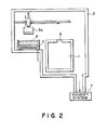
- Figure 2 is a schematic view for illustrating a second embodiment of the process and apparatus for producing a liquid crystal panel according to the present invention.
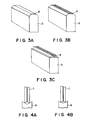
- Figures 3A - 3C are perspective views each illustrating the shape of a part for transferring a liquid crystal of a transfer member.
- Figures 4A and 4B are partial enlarged views each showing a part for applying a liquid crystal of a transfer member.
- a transfer member having a transfer part (end) with a length which is longer than the length of an injection port of a liquid crystal panel and shorter than the face of the liquid crystal panel having the injection port is used.
- the transfer part of the transfer member is dipped in a liquid crystal reservoir, is pulled up from the liquid crystal reservoir to apply the liquid crystal within the liquid crystal reservoir onto the transfer member and is then brought in close proximity to or in contact with the injection port of the liquid crystal panel so as to transfer the liquid crystal to the injection port.
- the injection port of the liquid crystal panel can be completely covered by the liquid crystal with minimum attachment of the liquid crystal to an unnecessary part of the liquid crystal panel.
- the vacuum chamber is restored to the atmospheric pressure to inject the liquid crystal into the liquid crystal panel.
- the above-mentioned transfer step can be further stabilized. More specifically, it is preferred to heat the transfer member, the injection port of the liquid crystal panel and the liquid crystal reservoir, so as to provide a temperature T1 for the liquid crystal in the liquid crystal reservoir, a temperature T2 for the transfer member and a temperature T3 for the injection port of the liquid crystal panel, satisfying the relationship of: T1 ⁇ T3 ⁇ T2.
- a ferroelectric liquid crystal generally has a high viscosity, so that it is desirable to utilize a temperature difference between two members in transferring or applying the liquid crystal to control the movement of the liquid crystal.
- a liquid crystal material is generally a mixture comprising many mesomorphic compounds, so that it is necessary to prevent a change or localization in composition within the liquid crystal reservoir. For this reason, it is desirable to heat the liquid crystal reservoir to an elevated temperature to lower the viscosity of the liquid crystal in the reservoir.
- T3 Under a higher injection temperature, i.e., a higher T3, it is possible to prevent the invasion of air bubbles at a higher degree because of a lower viscosity, so that a higher T3 is generally preferred. Too high T3 however leads to a problem of dropping of the liquid crystal from the liquid crystal panel. Therefore, it is desired that the upper limit of T3 is set to T1 to satisfy the relation of T1 ⁇ T3.
- T1, T2 and T3 so as to satisfy the relationship of T1 ⁇ T3 ⁇ T2.
- the present invention is applied to a ferroelectric liquid crystal material
- the ferroelectric liquid crystal can be selected from a large scope without particular restriction. For example,
- the transfer member may preferably have an end face having a length L2 for applying a liquid crystal to the injection port of the liquid crystal panel satisfying the relationship of L3 ⁇ L2 ⁇ L1 with respect to the liquid crystal panel which has a face including the injection port and having a length L1 and has the injection port having a length L3.
- L1 ⁇ L2 the liquid crystal attached to one or both sides is not applied to the liquid crystal panel but remains on the transfer member, thus resulting in difficulties such that it drips or requires a cleaning step and an unnecessary amount of liquid crystal is attached to a side face of the liquid crystal panel.
- L2 ⁇ L3 the injection port of the liquid crystal panel is not sufficiently covered with the applied liquid crystal, thus allowing air bubbles to enter the liquid crystal panel.
- Figures 3A - 3C respectively show some shapes of a part 8 (Figure 3A) or parts 8 ( Figure 3B and 3C) carrying and applying a liquid crystal of the transfer member 5 and particularly embodiments of the parts 8 ( Figures 3B and 3C) for simultaneously transferring the liquid crystal to a plurality of liquid crystal panels held in a cassette.
- Figures 4A and 4B are partially enlarged illustrations of two type of concavities formed at the top of a part 8 for transferring a liquid crystal for illustrating the operation of the part 8 corresponding to one shown in Figure 3B.
- the end face of a liquid crystal panel having an injection port is formed by bonding a pair of glass or plastic substrates after alignment at their ends which have been optionally formed by cutting.
- an injection port is positioned inward from utmost ends of the substrates, and it is preferred that the part 8 carrying and applying the liquid crystal of the transfer member is concave as shown in Figures 4A and 4B.
- Such a concavity has a function of automatically aligning the end face of the liquid crystal panel at the time of applying the liquid crystal to the liquid crystal panel.
- the concavity also has a function of effectively retaining the liquid crystal to prevent the liquid crystal from dripping.
- the pressure within the vacuum chamber after evacuation and for the liquid crystal transfer operation may desirably be 1.0x10 ⁇ 3 torr or below, preferably 1.0x10 ⁇ 5 torr or below.
- the injection of a liquid crystal into a liquid crystal panel is effectively carried out with minimum loss of the liquid crystal and alleviation of the load of washing of the liquid crystal as a post-treatment, and also the injection of a ferroelectric liquid crystal having a high viscosity can also be effected easily.
- Figure 1 is a schematic view of an embodiment of the apparatus for producing a liquid crystal panel according to the present invention.
- the apparatus includes, within a vacuum chamber 2, a liquid crystal panel 1 having at least one injection port 6, a liquid crystal reservoir 3 containing a liquid crystal 4, and a transfer member 5 which is moved between the liquid crystal reservoir 3 and the liquid crystal panel 1 for carrying a portion of the liquid crystal 4 in the liquid crystal reservoir 3 and applying the carried portion of the liquid crystal to the injection port 6 of the liquid crystal panel.
- the liquid crystal panel 1 is formed to have an end face having a length L1 and including the injection port 6 having a length L3
- the transfer member 5 is constituted to include an end face having a length L2 for applying the liquid crystal to the injection port of the liquid crystal panel, satisfying the relationship of L3 ⁇ L2 ⁇ L1.
- the liquid crystal 4 was a ferroelectric liquid crystal ("CS-1014", available from Chisso K.K.) showing the following phase transition series:
- the transfer member 5 was formed to have liquid crystal application parts 8 shown in Figure 3C and having a concavity as shown in Figure 4B.
- an exhaust system 7 conductively connected to a vacuum chamber 2 is first operated to evacuate the vacuum chamber 2 and the inside of the liquid crystal panel 1 contained therein.
- the transfer member 5 After a sufficient degree of evacuation to a pressure (e.g., 3x10 ⁇ 5 torr) within the vacuum chamber 2, the transfer member 5 is partly dipped in and then pulled out of the liquid crystal reservoir 3 to carry a portion of the liquid crystal 4. Then, the transfer member 5 is turned up side-down so as to direct the dipped end upward and then further moved upward to contact the injection port 6 of the liquid crystal panel 1, so that the injection port 6 is completely covered by the carried and transferred portion of the liquid crystal 4. Then, the vacuum chamber 2 is restored to the atmospheric pressure to effectively inject the liquid crystal inside the liquid crystal panel 1.
- a pressure e.g., 3x10 ⁇ 5 torr
- the heat generation from the heater 8 for the liquid crystal reservoir, the heater 11 for the transfer member and the heater 14 for the liquid crystal panel was controlled by annexed thermistors 9, 12 and 15, respectively, and a temperature controller 10.
- FIG 2 is a schematic view of another embodiment of the apparatus for producing a liquid crystal panel according to the present invention.
- like parts are denoted by like references numerals as used in Figure 1.
- Figure 2 shows an embodiment of the apparatus wherein a transfer member 5a after dipping for carrying a portion of a liquid crystal 4 within the liquid crystal reservoir 3 is moved to the injection port 6 of the liquid crystal panel 1 for transfer of the liquid crystal without turning or rotation thereof.
- the liquid crystal panel was also effectively filled with the liquid crystal.
- Liquid crystal panels were prepared similarly as in Example 1 except that L1, L2 and L3 were set to L3 ⁇ L1 ⁇ L2.
- a liquid crystal contained in a liquid crystal reservoir is applied to an injection port of a blank liquid crystal panel in a vacuum chamber, and the vacuum chamber is restored to the atmospheric pressure to inject the applied liquid crystal into the liquid crystal panel through the injection port.
- the liquid crystal particularly a ferroelectric liquid crystal having a high viscosity, is effectively used for filling the liquid crystal panel with a minimum loss by using a transfer member moving between the liquid crystal reservoir and the liquid crystal panel.
Landscapes
- Physics & Mathematics (AREA)
- Nonlinear Science (AREA)
- Mathematical Physics (AREA)
- Chemical & Material Sciences (AREA)
- Crystallography & Structural Chemistry (AREA)
- General Physics & Mathematics (AREA)
- Optics & Photonics (AREA)
- Liquid Crystal (AREA)
Applications Claiming Priority (2)
| Application Number | Priority Date | Filing Date | Title |
|---|---|---|---|
| JP2131271A JP2808478B2 (ja) | 1990-05-23 | 1990-05-23 | 液晶パネルの製造方法およびその装置 |
| JP131271/90 | 1990-05-23 |
Publications (3)
| Publication Number | Publication Date |
|---|---|
| EP0458321A2 true EP0458321A2 (fr) | 1991-11-27 |
| EP0458321A3 EP0458321A3 (en) | 1992-05-13 |
| EP0458321B1 EP0458321B1 (fr) | 1995-10-18 |
Family
ID=15054030
Family Applications (1)
| Application Number | Title | Priority Date | Filing Date |
|---|---|---|---|
| EP91108329A Expired - Lifetime EP0458321B1 (fr) | 1990-05-23 | 1991-05-22 | Procédé et dispositif pour fabriquer un écran à cristal liquide |
Country Status (8)
| Country | Link |
|---|---|
| US (2) | US5269351A (fr) |
| EP (1) | EP0458321B1 (fr) |
| JP (1) | JP2808478B2 (fr) |
| KR (1) | KR950014501B1 (fr) |
| AT (1) | ATE129349T1 (fr) |
| AU (1) | AU641248B2 (fr) |
| CA (1) | CA2042949C (fr) |
| DE (1) | DE69113864T2 (fr) |
Cited By (3)
| Publication number | Priority date | Publication date | Assignee | Title |
|---|---|---|---|---|
| EP0590291A3 (fr) * | 1992-08-19 | 1995-04-26 | Canon Kk | Procédé de fabrication d'un panneau à cristal liquide. |
| FR2752954A1 (fr) * | 1996-08-30 | 1998-03-06 | Lg Electronics Inc | Dispositif et procede d'injection de cristal liquide dans un panneau a cristal liquide |
| US6844908B2 (en) | 2000-10-04 | 2005-01-18 | Samsung Electronics Co., Ltd. | Apparatus for injecting liquid crystal materials and methods for manufacturing liquid crystal panels by using the same |
Families Citing this family (27)
| Publication number | Priority date | Publication date | Assignee | Title |
|---|---|---|---|---|
| JP2808478B2 (ja) * | 1990-05-23 | 1998-10-08 | キヤノン株式会社 | 液晶パネルの製造方法およびその装置 |
| US5406989A (en) * | 1993-10-12 | 1995-04-18 | Ayumi Industry Co., Ltd. | Method and dispenser for filling liquid crystal into LCD cell |
| US5507323A (en) * | 1993-10-12 | 1996-04-16 | Fujitsu Limited | Method and dispenser for filling liquid crystal into LCD cell |
| JP2814168B2 (ja) * | 1992-07-27 | 1998-10-22 | キヤノン株式会社 | 液晶の注入方法 |
| JP2805419B2 (ja) * | 1992-07-27 | 1998-09-30 | キヤノン株式会社 | 強誘電性液晶の注入方法 |
| US5548428A (en) * | 1992-07-27 | 1996-08-20 | Canon Kabushiki Kaisha | Process for injecting ferroelectric liquid crystal with injection completed above atmospheric pressure |
| US5546998A (en) * | 1992-12-25 | 1996-08-20 | Canon Kabushiki Kaisha | Apparatus for vacuum injecting liquid crystal |
| JP2824819B2 (ja) * | 1992-12-25 | 1998-11-18 | キヤノン株式会社 | 液晶注入方法及び注入装置 |
| US5477349A (en) * | 1993-04-27 | 1995-12-19 | Casio Computer Co., Ltd. | Liquid crystal injecting method |
| KR100321256B1 (ko) * | 1995-02-27 | 2002-06-20 | 윤종용 | 액정광학소자의제조방법및그에의해서수득된액정광학소자 |
| US5659377A (en) * | 1995-11-30 | 1997-08-19 | Lucent Technologies Inc. | Apparatus and method for filling liquid crystal display cells |
| JPH09265100A (ja) * | 1996-01-26 | 1997-10-07 | Matsushita Electric Ind Co Ltd | 液晶材料注入方法及び装置 |
| JPH09218416A (ja) * | 1996-02-09 | 1997-08-19 | Ayumi Kogyo Kk | 液晶の注入方法およびその装置 |
| KR100468147B1 (ko) * | 1996-03-12 | 2005-05-03 | 가부시키가이샤 베르덱스 | 액정충전방법 |
| JP3654483B2 (ja) * | 1997-10-09 | 2005-06-02 | 富士写真フイルム株式会社 | 液晶表示装置の製造方法 |
| US6561231B2 (en) | 1999-10-13 | 2003-05-13 | Armand P. Neukermans | Method for filling acoustic implantable transducers |
| KR100583310B1 (ko) * | 2000-01-19 | 2006-05-25 | 엘지.필립스 엘시디 주식회사 | 액정 주입/봉지 장치 및 방법 |
| WO2003037212A2 (fr) | 2001-10-30 | 2003-05-08 | Lesinski George S | Procede d'implantation dans la cochlee d'un element de commande microscopique de prothese auditive |
| US6619334B2 (en) * | 2001-11-29 | 2003-09-16 | Eastman Kodak Company | Method of delivering fluid into constricted openings free of voids |
| US7027122B2 (en) * | 2002-03-12 | 2006-04-11 | Lg.Philips Lcd Co., Ltd. | Bonding apparatus having compensating system for liquid crystal display device and method for manufacturing the same |
| TWI322287B (en) * | 2004-06-15 | 2010-03-21 | Hannstar Display Corp | Fabrication method of a liquid crystal display panel |
| TWI330729B (en) * | 2006-12-07 | 2010-09-21 | Au Optronics Corp | Liquid crystal injection method and liquid crystal tray thereof |
| CN101582363A (zh) * | 2008-05-14 | 2009-11-18 | 清华大学 | 真空器件的封接方法 |
| CN101587808B (zh) * | 2008-05-23 | 2011-06-08 | 清华大学 | 真空器件的封接装置以及封接方法 |
| CN101587807B (zh) * | 2008-05-23 | 2011-05-04 | 清华大学 | 真空器件的封接装置以及封接方法 |
| CN102096249B (zh) * | 2011-01-20 | 2012-03-21 | 深圳市宇顺电子股份有限公司 | 一种液晶注入方法 |
| CN104977760A (zh) * | 2014-04-08 | 2015-10-14 | 麒麟电子(深圳)有限公司 | 一种液晶灌注设备及灌注方法 |
Family Cites Families (12)
| Publication number | Priority date | Publication date | Assignee | Title |
|---|---|---|---|---|
| JPS5840726B2 (ja) * | 1975-11-12 | 1983-09-07 | 株式会社日立製作所 | 液晶封入装置 |
| US4586647A (en) * | 1983-07-15 | 1986-05-06 | Dearman Timothy Charles | Pipe clamps |
| EP0187425B1 (fr) * | 1985-01-02 | 1989-11-15 | International Business Machines Corporation | Cellule électro-optique et méthode pour sa fabrication |
| JPH0245170B2 (ja) * | 1985-08-01 | 1990-10-08 | Seiko Instr & Electronics | Sumekuteitsukuekishosochiniokeruekishobutsushitsuchunyuhoho |
| US4922972A (en) * | 1987-03-26 | 1990-05-08 | Semiconductor Energy Laboratory Co., Ltd. | Method of filling a liquid crystal device with liquid crystal |
| US4753276A (en) * | 1987-05-19 | 1988-06-28 | Central Glass Company, Limited | Method and apparatus for injecting liquid into display device cell |
| US4753267A (en) * | 1987-06-08 | 1988-06-28 | Eaton Corporation | Refrigeration valve |
| US5141036A (en) * | 1987-07-27 | 1992-08-25 | Semiconductor Energy Laboratory Co., Ltd. | Method of filling a liquid crystal device with introduction of liquid crystal by increasing pressure |
| DE3911359A1 (de) * | 1989-04-07 | 1990-10-11 | Nokia Unterhaltungselektronik | Verfahren zum befuellen einer fluessigkristallzelle |
| JP2808478B2 (ja) * | 1990-05-23 | 1998-10-08 | キヤノン株式会社 | 液晶パネルの製造方法およびその装置 |
| US5137484A (en) * | 1991-06-13 | 1992-08-11 | Proxima Corporation | Method of making a liquid crystal display construction |
| JPH06230219A (ja) * | 1993-01-29 | 1994-08-19 | Jasco Corp | 多層膜誘電体フィルターの製造装置及び製造方法 |
-
1990
- 1990-05-23 JP JP2131271A patent/JP2808478B2/ja not_active Expired - Fee Related
-
1991
- 1991-05-17 US US07/701,998 patent/US5269351A/en not_active Expired - Fee Related
- 1991-05-21 CA CA002042949A patent/CA2042949C/fr not_active Expired - Fee Related
- 1991-05-22 AU AU77271/91A patent/AU641248B2/en not_active Ceased
- 1991-05-22 DE DE69113864T patent/DE69113864T2/de not_active Expired - Fee Related
- 1991-05-22 AT AT91108329T patent/ATE129349T1/de not_active IP Right Cessation
- 1991-05-22 EP EP91108329A patent/EP0458321B1/fr not_active Expired - Lifetime
- 1991-05-23 KR KR1019910008386A patent/KR950014501B1/ko not_active Expired - Fee Related
-
1994
- 1994-09-08 US US08/303,002 patent/US5564479A/en not_active Expired - Fee Related
Cited By (6)
| Publication number | Priority date | Publication date | Assignee | Title |
|---|---|---|---|---|
| EP0590291A3 (fr) * | 1992-08-19 | 1995-04-26 | Canon Kk | Procédé de fabrication d'un panneau à cristal liquide. |
| US5479284A (en) * | 1992-08-19 | 1995-12-26 | Canon Kabushiki Kaisha | Increasing temperature injection methods for a liquid crystal cell |
| US5576865A (en) * | 1992-08-19 | 1996-11-19 | Canon Kabushiki Kaisha | Process for producing liquid crystal panel including reducing the pressure to no more than 25 torr/minute |
| US5699138A (en) * | 1992-08-19 | 1997-12-16 | Canon Kabushiki Kaisha | Process for injecting liquid crystal into a liquid crystal panel |
| FR2752954A1 (fr) * | 1996-08-30 | 1998-03-06 | Lg Electronics Inc | Dispositif et procede d'injection de cristal liquide dans un panneau a cristal liquide |
| US6844908B2 (en) | 2000-10-04 | 2005-01-18 | Samsung Electronics Co., Ltd. | Apparatus for injecting liquid crystal materials and methods for manufacturing liquid crystal panels by using the same |
Also Published As
| Publication number | Publication date |
|---|---|
| US5564479A (en) | 1996-10-15 |
| DE69113864D1 (de) | 1995-11-23 |
| ATE129349T1 (de) | 1995-11-15 |
| KR910020476A (ko) | 1991-12-20 |
| EP0458321A3 (en) | 1992-05-13 |
| JPH0426823A (ja) | 1992-01-30 |
| US5269351A (en) | 1993-12-14 |
| EP0458321B1 (fr) | 1995-10-18 |
| KR950014501B1 (ko) | 1995-12-02 |
| AU7727191A (en) | 1992-01-02 |
| CA2042949C (fr) | 1996-01-09 |
| JP2808478B2 (ja) | 1998-10-08 |
| AU641248B2 (en) | 1993-09-16 |
| DE69113864T2 (de) | 1996-04-04 |
| CA2042949A1 (fr) | 1991-11-24 |
Similar Documents
| Publication | Publication Date | Title |
|---|---|---|
| EP0458321B1 (fr) | Procédé et dispositif pour fabriquer un écran à cristal liquide | |
| JP2814171B2 (ja) | 液晶パネルの製造方法 | |
| US5548428A (en) | Process for injecting ferroelectric liquid crystal with injection completed above atmospheric pressure | |
| US4917473A (en) | Method of manufacturing liquid crystal devices | |
| JPS6431118A (en) | Method for injecting liquid crystal exhibiting ferroelectric property | |
| US5029623A (en) | Process for filling a liquid crystal cell | |
| US4922974A (en) | Method of filling a liquid crystal device with liquid crystal | |
| US5684556A (en) | Process for producing liquid crystal device | |
| EP0570804B1 (fr) | Procédé d'injection d'un cristal liquide ferroélectrique | |
| US5417257A (en) | Method and apparatus for injecting liquid crystal | |
| US5108332A (en) | Method of manufacturing a liquid-crystal cell | |
| KR930006761B1 (ko) | 고체표면상에 박유체막을 코팅하는 방법과 장치 | |
| US5953095A (en) | Liquid crystal cell and method of manufacturing the same | |
| JP3108963B2 (ja) | 強誘電性液晶素子の製造方法 | |
| KR100574276B1 (ko) | 상변화 액정주입장치 | |
| JP4166848B2 (ja) | 液晶注入装置及び方法 | |
| JPH0483228A (ja) | 液晶表示装置の製造装置 | |
| JPS638630A (ja) | 液晶注入方法 | |
| JPH0961831A (ja) | 液晶表示素子の液晶注入方法および液晶注入装置 | |
| JPS5754919A (en) | Liquid crystal element | |
| JPH0850294A (ja) | 液晶素子の製造方法 | |
| JPH0571559B2 (fr) | ||
| JPS6262329A (ja) | 液晶表示素子の製造方法 | |
| JPS57141617A (en) | Manufacture of liquid crystal display cell | |
| JPS6484223A (en) | Method for orientating liquid crystal display element |
Legal Events
| Date | Code | Title | Description |
|---|---|---|---|
| PUAI | Public reference made under article 153(3) epc to a published international application that has entered the european phase |
Free format text: ORIGINAL CODE: 0009012 |
|
| 17P | Request for examination filed |
Effective date: 19910621 |
|
| AK | Designated contracting states |
Kind code of ref document: A2 Designated state(s): AT BE CH DE DK ES FR GB GR IT LI LU NL SE |
|
| PUAL | Search report despatched |
Free format text: ORIGINAL CODE: 0009013 |
|
| AK | Designated contracting states |
Kind code of ref document: A3 Designated state(s): AT BE CH DE DK ES FR GB GR IT LI LU NL SE |
|
| 17Q | First examination report despatched |
Effective date: 19931230 |
|
| GRAA | (expected) grant |
Free format text: ORIGINAL CODE: 0009210 |
|
| AK | Designated contracting states |
Kind code of ref document: B1 Designated state(s): AT BE CH DE DK ES FR GB GR IT LI LU NL SE |
|
| PG25 | Lapsed in a contracting state [announced via postgrant information from national office to epo] |
Ref country code: LI Effective date: 19951018 Ref country code: GR Free format text: LAPSE BECAUSE OF FAILURE TO SUBMIT A TRANSLATION OF THE DESCRIPTION OR TO PAY THE FEE WITHIN THE PRESCRIBED TIME-LIMIT Effective date: 19951018 Ref country code: ES Free format text: THE PATENT HAS BEEN ANNULLED BY A DECISION OF A NATIONAL AUTHORITY Effective date: 19951018 Ref country code: DK Effective date: 19951018 Ref country code: CH Effective date: 19951018 Ref country code: BE Effective date: 19951018 Ref country code: AT Effective date: 19951018 |
|
| REF | Corresponds to: |
Ref document number: 129349 Country of ref document: AT Date of ref document: 19951115 Kind code of ref document: T |
|
| REF | Corresponds to: |
Ref document number: 69113864 Country of ref document: DE Date of ref document: 19951123 |
|
| ITF | It: translation for a ep patent filed | ||
| PG25 | Lapsed in a contracting state [announced via postgrant information from national office to epo] |
Ref country code: SE Effective date: 19960118 |
|
| ET | Fr: translation filed | ||
| REG | Reference to a national code |
Ref country code: CH Ref legal event code: PL |
|
| PG25 | Lapsed in a contracting state [announced via postgrant information from national office to epo] |
Ref country code: LU Free format text: LAPSE BECAUSE OF NON-PAYMENT OF DUE FEES Effective date: 19960531 |
|
| PLBE | No opposition filed within time limit |
Free format text: ORIGINAL CODE: 0009261 |
|
| STAA | Information on the status of an ep patent application or granted ep patent |
Free format text: STATUS: NO OPPOSITION FILED WITHIN TIME LIMIT |
|
| 26N | No opposition filed | ||
| REG | Reference to a national code |
Ref country code: GB Ref legal event code: IF02 |
|
| PGFP | Annual fee paid to national office [announced via postgrant information from national office to epo] |
Ref country code: FR Payment date: 20030508 Year of fee payment: 13 |
|
| PGFP | Annual fee paid to national office [announced via postgrant information from national office to epo] |
Ref country code: GB Payment date: 20030519 Year of fee payment: 13 |
|
| PGFP | Annual fee paid to national office [announced via postgrant information from national office to epo] |
Ref country code: DE Payment date: 20030529 Year of fee payment: 13 |
|
| PGFP | Annual fee paid to national office [announced via postgrant information from national office to epo] |
Ref country code: NL Payment date: 20030530 Year of fee payment: 13 |
|
| PG25 | Lapsed in a contracting state [announced via postgrant information from national office to epo] |
Ref country code: GB Free format text: LAPSE BECAUSE OF NON-PAYMENT OF DUE FEES Effective date: 20040522 |
|
| PG25 | Lapsed in a contracting state [announced via postgrant information from national office to epo] |
Ref country code: NL Free format text: LAPSE BECAUSE OF NON-PAYMENT OF DUE FEES Effective date: 20041201 Ref country code: DE Free format text: LAPSE BECAUSE OF NON-PAYMENT OF DUE FEES Effective date: 20041201 |
|
| GBPC | Gb: european patent ceased through non-payment of renewal fee |
Effective date: 20040522 |
|
| PG25 | Lapsed in a contracting state [announced via postgrant information from national office to epo] |
Ref country code: FR Free format text: LAPSE BECAUSE OF NON-PAYMENT OF DUE FEES Effective date: 20050131 |
|
| NLV4 | Nl: lapsed or anulled due to non-payment of the annual fee |
Effective date: 20041201 |
|
| REG | Reference to a national code |
Ref country code: FR Ref legal event code: ST |
|
| PG25 | Lapsed in a contracting state [announced via postgrant information from national office to epo] |
Ref country code: IT Free format text: LAPSE BECAUSE OF NON-PAYMENT OF DUE FEES;WARNING: LAPSES OF ITALIAN PATENTS WITH EFFECTIVE DATE BEFORE 2007 MAY HAVE OCCURRED AT ANY TIME BEFORE 2007. THE CORRECT EFFECTIVE DATE MAY BE DIFFERENT FROM THE ONE RECORDED. Effective date: 20050522 |