EP0459380B1 - Dispositif de mémoire statique à semi-conducteurs - Google Patents
Dispositif de mémoire statique à semi-conducteurs Download PDFInfo
- Publication number
- EP0459380B1 EP0459380B1 EP91108662A EP91108662A EP0459380B1 EP 0459380 B1 EP0459380 B1 EP 0459380B1 EP 91108662 A EP91108662 A EP 91108662A EP 91108662 A EP91108662 A EP 91108662A EP 0459380 B1 EP0459380 B1 EP 0459380B1
- Authority
- EP
- European Patent Office
- Prior art keywords
- power source
- memory cell
- source wiring
- memory device
- static semiconductor
- Prior art date
- Legal status (The legal status is an assumption and is not a legal conclusion. Google has not performed a legal analysis and makes no representation as to the accuracy of the status listed.)
- Expired - Lifetime
Links
- 230000003068 static effect Effects 0.000 title claims description 28
- 239000004065 semiconductor Substances 0.000 title claims description 27
- 229910021420 polycrystalline silicon Inorganic materials 0.000 claims description 53
- 239000003990 capacitor Substances 0.000 claims description 17
- XAGFODPZIPBFFR-UHFFFAOYSA-N aluminium Chemical compound [Al] XAGFODPZIPBFFR-UHFFFAOYSA-N 0.000 claims description 14
- 229910052782 aluminium Inorganic materials 0.000 claims description 14
- 239000010409 thin film Substances 0.000 claims description 10
- 238000007599 discharging Methods 0.000 claims description 3
- 239000010410 layer Substances 0.000 description 32
- 238000009792 diffusion process Methods 0.000 description 20
- 239000010408 film Substances 0.000 description 19
- 238000010276 construction Methods 0.000 description 10
- 238000010586 diagram Methods 0.000 description 10
- 239000000758 substrate Substances 0.000 description 7
- 239000012535 impurity Substances 0.000 description 6
- XUIMIQQOPSSXEZ-UHFFFAOYSA-N Silicon Chemical compound [Si] XUIMIQQOPSSXEZ-UHFFFAOYSA-N 0.000 description 4
- 230000002159 abnormal effect Effects 0.000 description 4
- 230000003071 parasitic effect Effects 0.000 description 4
- 229910052710 silicon Inorganic materials 0.000 description 4
- 239000010703 silicon Substances 0.000 description 4
- 238000009413 insulation Methods 0.000 description 3
- 230000002950 deficient Effects 0.000 description 2
- 230000003292 diminished effect Effects 0.000 description 2
- 239000011229 interlayer Substances 0.000 description 2
- 230000003647 oxidation Effects 0.000 description 2
- 238000007254 oxidation reaction Methods 0.000 description 2
- 229910021417 amorphous silicon Inorganic materials 0.000 description 1
- 230000008878 coupling Effects 0.000 description 1
- 238000010168 coupling process Methods 0.000 description 1
- 238000005859 coupling reaction Methods 0.000 description 1
- 230000006870 function Effects 0.000 description 1
- 230000036039 immunity Effects 0.000 description 1
- 230000010354 integration Effects 0.000 description 1
- 239000011159 matrix material Substances 0.000 description 1
- 238000000034 method Methods 0.000 description 1
- 238000012986 modification Methods 0.000 description 1
- 230000004048 modification Effects 0.000 description 1
- 239000002245 particle Substances 0.000 description 1
- 239000007787 solid Substances 0.000 description 1
Images


Classifications
-
- G—PHYSICS
- G11—INFORMATION STORAGE
- G11C—STATIC STORES
- G11C11/00—Digital stores characterised by the use of particular electric or magnetic storage elements; Storage elements therefor
- G11C11/21—Digital stores characterised by the use of particular electric or magnetic storage elements; Storage elements therefor using electric elements
- G11C11/34—Digital stores characterised by the use of particular electric or magnetic storage elements; Storage elements therefor using electric elements using semiconductor devices
- G11C11/40—Digital stores characterised by the use of particular electric or magnetic storage elements; Storage elements therefor using electric elements using semiconductor devices using transistors
- G11C11/41—Digital stores characterised by the use of particular electric or magnetic storage elements; Storage elements therefor using electric elements using semiconductor devices using transistors forming static cells with positive feedback, i.e. cells not needing refreshing or charge regeneration, e.g. bistable multivibrator or Schmitt trigger
-
- G—PHYSICS
- G11—INFORMATION STORAGE
- G11C—STATIC STORES
- G11C5/00—Details of stores covered by group G11C11/00
- G11C5/14—Power supply arrangements, e.g. power down, chip selection or deselection, layout of wirings or power grids, or multiple supply levels
- G11C5/147—Voltage reference generators, voltage or current regulators; Internally lowered supply levels; Compensation for voltage drops
-
- G—PHYSICS
- G11—INFORMATION STORAGE
- G11C—STATIC STORES
- G11C11/00—Digital stores characterised by the use of particular electric or magnetic storage elements; Storage elements therefor
- G11C11/21—Digital stores characterised by the use of particular electric or magnetic storage elements; Storage elements therefor using electric elements
- G11C11/34—Digital stores characterised by the use of particular electric or magnetic storage elements; Storage elements therefor using electric elements using semiconductor devices
- G11C11/40—Digital stores characterised by the use of particular electric or magnetic storage elements; Storage elements therefor using electric elements using semiconductor devices using transistors
- G11C11/41—Digital stores characterised by the use of particular electric or magnetic storage elements; Storage elements therefor using electric elements using semiconductor devices using transistors forming static cells with positive feedback, i.e. cells not needing refreshing or charge regeneration, e.g. bistable multivibrator or Schmitt trigger
- G11C11/412—Digital stores characterised by the use of particular electric or magnetic storage elements; Storage elements therefor using electric elements using semiconductor devices using transistors forming static cells with positive feedback, i.e. cells not needing refreshing or charge regeneration, e.g. bistable multivibrator or Schmitt trigger using field-effect transistors only
Definitions
- the present invention relates to a static semiconductor memory device comprising a memory cell using a thin film transistor as a load element.
- SRAM static semiconductor memory device
- CMOS memory cell utilizing p-channel and n-channel MOS transistors formed in a silicon substrate or in a well region of the silicon substrate as a load transistor and a driving transistor, respectively, and a memory cell using a polycrystalline silicon of a high resistivity as a load element.
- a marked increase in the capacity has been achieved nowadays in the memory device comprising a memory cell using a polycrystalline silicon of a high resistivity as a load element.
- the polycrystalline silicon used in a memory cell of this type has a resistance as high as several tera ohms (10 12 ⁇ ) in order to keep the current consumption as low as possible during the rest time, i.e., when any of memory cells is not selected.
- the amount of the signal charge supplied to a data memory node within the memory cell is very small. This causes a problem when current leaks from the data memory node through, for example, a PN junction, an insulating film or a transistor.
- the signal charge precharged on the data memory node is more released than that supplied from a load element, that is, data is more liable to be destroyed.
- leak current takes place in only one of a large number of memory cells included in a memory device. In this case, the defective memory cell lowers the reliability of the entire memory cell.
- TFT thin film transistor
- the TFT is a transistor having the channel region formed in a thin polycrystalline silicon film, not in a silicon substrate.
- the TFT can be formed in a stacked manner on an ordinary MOS transistor (bulk transistor) having the channel region formed in a silicon substrate.
- the complete CMOS memory cell can be formed with a cell area substantially equal to that of the conventional memory cell using a polycrystalline silicon as a load resistor.
- the static memory cell using a TFT as a load element is complete CMOS memory cell.
- the memory cell using a TFT permits a high degree of integration like the memory cell using a polycrystalline silicon and also permits a low power consumption and a stable operation like the complete CMOS memory cell.
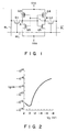
- Fig. 1 is an equivalent circuit diagram showing a static memory cell using a TFT. It is seen that the memory cell comprises two transfer gates consisting of N-channel MOS transistors Q1 and Q2, respectively. A bit line BL is connected to one end of the transistor Q1 (transfer gate), and another bit line /BL to one end of the transistor Q2 (transfer gate). The other ends of these transistors Q1, Q2 are connected to inner memory nodes (data storing nodes) A and B, respectively. Further, the gates of the transistors Q1 and Q2 are commonly connected to a word line WL.
- the inner memory node A Connected to the inner memory node A are the drain of an N-channel MOS transistor Q3 and the drain of a P-channel TFT Q4. The gates of these transistors Q3 and Q4 are commonly connected to the other inner memory node B. Also connected to the node B are the drain of an N-channel MOS transistor Q5 and the drain of a TFT Q6. The gates of these transistors Q5 and Q6 are commonly connected to the inner memory node A.
- the sources of the transistors Q4 and Q6 are connected to a supply node of a power source potential Vcc, with the sources of the transistors Q3 and Q5 being connected to a supply node of a ground potential Vss.
- the transistors Q3 and Q4 form a CMOS inverter.
- transistors Q5 and Q6 form a CMOS inverter.
- the TFT used as a load element of each of these CMOS inverters functions as a transistor, with the result that current hardly flows to the inner memory node when the TFT is turned off.
- an oncurrent which is sufficiently large compared with the memory cell using a load element of a high resistance, flows to the inner memory node.
- Fig. 2 shows the relationship between the gate voltage VG (volt) and the drain current ID (ampere) in a typical TFT sized, for example, at 1.5 ⁇ m in the channel length, 0.5 ⁇ m in the channel width, 25 nm in the thickness of the gate insulation film and 36 nm in the thickness of the polycrystalline silicon layer in which is formed the channel region.
- the drain voltage is set at -4 V.
- the drain current is about 10 -13 (A) when the TFT is turned off, with the gate voltage VG set at 0 V.
- the drain current is about 10 -7 (A) when the gate voltage is set at -4 V so as to turn the TFT on. It follows that the TFT exhibits an on/off current ratio of about 6 figures, i.e., a resistance ratio of about 6 figures.
- each of the inner memory nodes A and B of the memory cell is accompanied by a parasitic capacitance (not shown).
- the parasitic capacitance tends to be diminished in accordance with the scaling of the memory cell size.
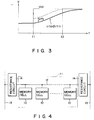
- Fig. 3 shows a change in the potential within the memory cell.
- a symbol " ⁇ 1" shown in the drawing denotes a time constant of the potential Vnod in the case where the inner memory node A or B is charged by the on-current of the TFT.
- the potential difference between the power source potential Vcc and the potential Vnod is greater than the threshold voltage Vth of the P-channel TFT.
- the TFT which should originally be turned off, is also turned on, with the result that this TFT is connected in series to the TFT which is turned from off-state to on-state. It follows that current flows through the N-channel MOS transistor, which is already in an on-state, for a predetermined period of time, i.e., about 100 ns as noted previously. It should be noted that a TFT, which is turned off, is always included in each memory cell. Thus, current of at least 10 -1 A, i.e., 100 mA, flows through the memory cell array when it comes to an SRAM of a large capacity, e.g., at least 4M bits (4 ⁇ 10 6 bits). Since the average operating current of the ordinary SRAM is less than 100 mA, the current exceeding 100 mA which flows during the power source bump through an SRAM of 4 M bits or more becomes an abnormal current far exceeding the allowable limit.
- the power source wiring positions, within the memory cell array for supplying the power source potential to each memory cell is formed of a polycrystalline silicon.
- a resistance component and a stray capacitance component are included in the power source wiring formed of the polycrystalline silicon.
- the power source wiring positioned within the memory cell array can be regarded as a delay line.
- that portion of the power source wiring for supplying the power source potential to each memory cell which is positioned outside the memory cell array is generally formed of aluminum.
- the power source wiring formed of aluminum is electrically connected within the memory cell array to the power source wiring formed of polycrystalline silicon, which is positioned within the memory cell array.
- the polycrystalline silicon wiring can be regarded as a delay line.
- the resistivity of the aluminum wiring is very low. It follows that the time constant of the polycrystalline silicon wiring is diminished with respect to the memory cell positioned closer to the connecting point between the aluminum wiring and the polycrystalline silicon wiring, with the result that a greater DC current flows through said memory cell during the power source bump.
- the conventional static semiconductor memory device using a TFT as a load element within the memory cell is defective in that an abnormal current flows through each memory cell during the power source bump, leading to an increased power consumption.
- EP-A-0 348 895 shows a device with a low noise power supply structure. Memory cells are connected to ground via an impedance element to reduce noise.
- US-A-4 805 147 shows providing capacitors connected to storage nodes in a memory device to improve alpha particle immunity.
- An object of the present invention is to provide a static semiconductor memory device, which permits preventing the flow of an abnormal current through each memory cell during the power source bump so as to diminish the power consumption.
- a static semiconductor memory device as set out in claim 1.
- Fig. 4 is a block diagram showing the construction of a static semiconductor memory device according to a first embodiment of the present invention.
- the memory device comprises a plurality of memory cells 10, which are aligned in, for example, series to form a memory cell array 11.
- these memory cells 10 are arranged to form a matrix within the memory cell array 11, though only a single row of memory cells 10 are shown in the drawing.
- Each memory cell 10 is electrically connected to a power source wiring 12 positioned within the memory cell array 11.
- the wiring 12 is formed of, for example, polycrystalline silicon.
- a power source potential Vcc on the high potential side is supplied through the power source wiring 12 to each memory cell 10.
- the memory device also comprises another power source wiring 13 of a low resistance formed of, for example, aluminum and positioned outside the memory cell array. The power source potential Vcc from the outside is supplied through the aluminum wiring 13 to each part of the entire memory device.
- the power source wiring 12 positioned within the memory cell array is electrically connected via a resistor circuit 14 to the aluminum power source wiring 13.
- Fig. 5 shows in detail the construction of one of the memory cells and the resistor circuit 14 included in the block diagram shown in Fig. 4.
- the memory cell 10 comprises transfer gates Q1 to Q2 each formed of an N-channel MOS transistor, N-channel MOS transistor Q3, Q5, and P-channel TFTs Q4, Q6.
- the memory cell also comprises inner memory nodes A and B as in the prior art shown in Fig. 1. Further, memory capacitors C1 and C2 are equivalently connected to the inner memory nodes A and B, respectively.
- the source of each of the TFTs Q4 and Q6 is connected to the power source wiring 12 formed of polycrystalline silicon.
- the power source potential Vcc on the high potential side is supplied through the polycrystalline silicon wiring 12 to each memory cell 10.
- a parasitic resistance component 15 and a stray capacitance component 16 reside in the polycrystalline silicon wiring 12, as shown in Fig. 5.
- Each of the resistance circuits 14 can be formed of, for example, a polycrystalline silicon having a high resistivity or a TFT equal in construction to the TFT Q4 or Q6 included in the memory cell 10.
- the resistance circuit 14 is formed of a TFT 17 having the gate connected to the ground potential Vss.
- the resistance of the TFT 17 is set to meet the relationship ⁇ 2 ⁇ ⁇ 1, in which ⁇ 1 denotes a time constant in the case of charging the inner memory node A or B by the power source potential transmitted to the power source wiring 12 positioned within the memory cell array, and ⁇ 2 represents a time constant in the case of charging the power source wiring 12 by the power source potential transmitted to the aluminum power source wiring 13.
- the resistance of the TFT 17 can be changed by controlling, for example, the channel width or channel length of the TFT.
- the resistance circuit 14 serves to lower the charging rate of the power source wiring 12 positioned within the memory cell array, as apparent from the waveform shown in Fig. 6.
- the time constant ⁇ 2 is increased in this step.
- the inner memory node A or B included in each memory cell 10 is charged by the potential of the power source wiring 12 having a low charging rate.
- the charging rate of the capacitor C1 or C2 include in the inner memory node A or B is close to the charging rate of the power source wiring 12 positioned within the memory cell array.
- the TFT Q4 or Q6 which turned off, included in the memory cell 10 is not turned on in the case of the power source bump. It follows that it is possible to prevent a difficulty accompanying the conventional memory cell, i.e., flow of a DC current between the power source potential Vcc and the ground potential Vss.
- the on-resistance of the TFT 17 is equal to that of the TFT included in the memory cell. It should also be noted that the sum of the stray capacitance components 16 of the power source wiring 12 positioned within the memory cell array is greater than the capacitance C1, C2 within the memory cell so as to meet the relationship ⁇ 2 ⁇ ⁇ 1.
- Fig. 7 shows a memory device according to a second embodiment of the present invention.
- the resistance circuit 14 is formed of a resistance element 18 consisting of, for example, a polycrystalline silicon.
- the power source wiring 12 positioned within the memory cell array is also formed of a polycrystalline silicon.
- a p-type or N-type impurity is diffused into the polycrystalline silicon so as to lower the resistance of the power source wiring 12.
- the resistance element 18 noted above can be formed by diffusing a low concentration of an impurity element into a part of the polycrystalline silicon forming the power source wiring 12.
- Fig. 8 shows a memory device according to a third embodiment of the present invention.
- each of the resistance circuits 14 is formed of a P-channel enhancement type MOS transistor 19.
- the gate of the MOS transistor 19 is connected to the ground potential Vss. It should be noted that the resistance of the circuit 14 can be controlled by adjusting, for example, the channel width or the channel length of the MOS transistor 19.
- Fig. 9 is a circuit diagram showing the construction of a memory cell in a static semiconductor memory device according to a fourth embodiment of the present invention.
- a capacitance 21 substantially equal to the capacitance C1 of the inner memory node A included in the memory cell 10 is connected between the node A and the power source wiring 12 positioned within the memory cell array.
- another capacitance 21 substantially equal to the capacitance C2 of the inner memory node B is connected between the node B and the power source wiring 12.
- the potential of the power source wiring 13 positioned outside the memory cell array has been rapidly elevated in the stage of the power source bomb in the memory device of the construction described above.
- the potential of the power source wiring 12 positioned within the memory cell array has been elevated in accordance with elevation of the potential of the aluminum power source wiring 13
- the potential of the inner memory nodes A and B is also elevated because of the capacitive coupling of each of the capacitances 21.
- the difference between the gate potential of the TFT, which should originally be turned off, and the source potential of said TFT, which is equal to the potential of the power source wiring 12 positioned within the memory cell array is lower than the threshold voltage of the TFT, the TFT is kept turned off. In other words, it is necessary to determine the capacitance value of each of the capacitors 21 to meet the particular condition.
- the TFT Q4 or Q6 which is turned off, is prevented from being turned on, making it possible to prevent the difficulty accompanying the prior art, i.e., flow of a DC current through each memory cell between the power power source potential Vcc and the ground potential Vss.
- Figs. 10A and 10B show the specific construction of the memory cell used in the static semiconductor memory device according to the fourth embodiment of the present invention described above. Specifically, Fig. 10A is a plan view of the memory cell, and Fig. 10B is a cross sectional view along the line A-A' shown in Fig. 10A.
- the memory cell is prepared by adding the two capacitors 21 to the conventional memory cell using a TFT as a load.
- the memory cell comprises a P-type semiconductor substrate 31, a field insulation film 32, N+ diffusion regions 33 acting as source and drain regions of the N-channel MOS transistors Q1, Q2, Q3, and Q5 referred to previously, a first polycrystalline silicon layer 34 forming the gates of the N-channel MOS transistors Q1, Q2, Q3 and Q5, a second polycrystalline silicon layer 35 forming the gates of the P-channel TFTs Q4 and Q6, a third polycrystalline silicon layer 36 forming the channel regions as well as source and drain regions of the TFTs Q4 and Q6, and a channel region 37 of a TFT, said channel region 37 being formed within the third polycrystalline silicon layer 36.
- the channel region 37 is substantially free from an impurity and, thus, has a high resistivity.
- the word line WL as well as a power source line for supplying a ground potential Vss to each memory cell is formed of the first polycrystalline silicon layer 34.
- the power source wiring 12 positioned within the memory cell array is formed by utilizing the third polycrystalline silicon layer 36.
- the N + diffusion region is not shown in Fig. 10A.
- Fig. 10B does not show the insulating films interposed between the first polycrystalline silicon layer 34 and the substrate 31 and between the first and second polycrystalline silicon layers 34 and 35.
- Each of the capacitors 21 is provided by each of regions 38 in which the second and third polycrystalline silicon layers 35 and 36 are superposed one upon the other with an insulating film (not shown) interposed therebetween.
- the second polycrystalline silicon layer 35 constituting the gate of the TFT acts as one electrode of the capacitor 21
- Fig. 11A is a plan view showing the construction of a memory cell having the capacitor 21 added thereto
- Fig. 11B is a cross sectional view along the line B-B' shown in Fig. 11A.
- the memory cell shown in Fig. 11 comprises a P-type semiconductor substrate 41, a field insulation film 42, an N + diffusion region 43 providing the source or drain region of the N-channel MOS transistor Q1, an N + diffusion region 44 providing the drain or source region of the N-channel MOS transistor Q1, an N + diffusion region 45 providing the source or drain region of the N-channel MOS transistor Q2, an N + diffusion region 46 providing the drain or source region of the N-channel MOS transistor Q2 and drain region of the N-channel MOS transistor Q5, an N + diffusion region 47 providing the source region of the N-channel MOS transistor Q5, an N+ diffusion region 48 providing the drain region of the N-channel MOS transistor Q3, an N + diffusion region 49 providing the source region of the N-channel MOS transistor Q3, gates 50 of the N-channel MOS transistors
- the aluminum wiring layer 57 is connected to the N + diffusion region 43 via a contact hole 59.
- the other aluminum wiring layer 58 is connected to the N + diffusion region 45 via a contact hole 60.
- the N + diffusion region 44 is connected to the gate 51 of the N-channel MOS transistor Q5 via a contact hole 61.
- the gate 51 is connected to the second polycrystalline silicon layer 53 via a contact hole 62.
- the N + diffusion region 46 is connected to the gate 52 of the N-channel MOS transistor Q3 via a contact hole 63.
- the gate 52 is connected to the second polycrystalline silicon layer 53 via a contact hole 64.
- the N + diffusion region 48 providing the drain region of the N-channel MOS transistor Q3 is connected to the gate 51 of the N-channel MOS transistor Q5 via a contact hole 65.
- a P-type impurity element is introduced in a high concentration into most portion of the second polycrystalline silicon layer 53 so as to lower the resistivity of the polycrystalline silicon layer 53.
- an impurity is not positively introduced into that region 66 of the polycrystalline silicon layer 53 which faces the N + diffusion region 46 so as to keep the high resistivity in the region 66.
- the region 66 which acts as the channel region of the TFT Q4 is superposed upon the N + diffusion region 46 with a thermal oxide film 67 interposed therebetween, said oxide film 67 being formed by the thermal oxidation of said N + diffusion region region 46.
- a region 68 of the polycrystalline silicon layer 53, said region 68 facing the N + diffusion region 48, is substantially free from an impurity and, thus, exhibits a high resistivity.
- the region 68 which acts as the channel region of the TFT Q6, is superposed upon the N + diffusion region 48 with a thermal oxide film (not shown) interposed therebetween, said oxide film being formed by the thermal oxidation of said N + diffusion region region 48.
- Each of the capacitors 21 is provided by the region in which the second and third polycrystalline silicon layer 53 and 55 are superposed one upon the other with the insulating film 56 interposed therebetween.
- one electrode of the capacitor 21 is provided by the second polycrystalline silicon layer 53 in which is formed the channel region of the TFT.
- the other electrode is provided by the third polycrystalline silicon layer 55 which is set at the power source potential Vcc and positioned above the second polycrystalline silicon layer 53 with the insulating film 54 interposed therebetween.
- the present invention is not restricted to the embodiments described above. Of course, various modifications are available within the technical scope of the present invention.
- the power source voltage Vcc of a high potential is supplied to the power source wiring 12 positioned within the memory cell array so as to charge the inner memory nodes A and B by the potential of the wiring 12.
- a potential lower than the ground voltage Vss i.e., a negative potential
- the wiring 12 for operating the memory cell it is also possible to supply a potential lower than the ground voltage Vss, i.e., a negative potential, to the wiring 12 for operating the memory cell. In this case, the negative charge of the inner memory nodes A and B included in each memory cell is released into the wiring 12.
- the channel region of the TFT is formed in a thin polycrystalline silicon film in each of the first to fourth embodiments described above.
- the present invention provides a static semiconductor memory device which permits preventing an abnormal current from flowing through the memory cell during the power source bumb so as to diminish the current consumption.
Landscapes
- Engineering & Computer Science (AREA)
- Microelectronics & Electronic Packaging (AREA)
- Power Engineering (AREA)
- Computer Hardware Design (AREA)
- Semiconductor Memories (AREA)
- Thin Film Transistor (AREA)
- Static Random-Access Memory (AREA)
Claims (9)
- Dispositif de mémoire statique à semiconducteur comprenant une configuration de cellule de mémoire (11) constituée d'une pluralité de cellules de mémoire (10) possédant chacune un noeud de mémoire de données (A, B) et un transistor à film mince (Q4, Q6) utilisé comme transistor de charge et raccordé à une extrémité du noeud de mémoire et à l'autre extrémité à un potentiel de source de puissance (Vcc);un premier câblage de source de puissance (12) placé dans la configuration de cellule de mémoire et raccordé à chaque cellule de mémoire de façon à fournir ledit potentiel de source de puissance (Vcc) à chaque cellule de mémoire; etun second câblage de source de puissance (13) d'une faible résistance auquel ledit potentiel de source de puissance (Vcc) est fourni de l'extérieur et qui est électriquement raccordé au premier câblage de source de puissance;dispositif caractérisé par un moyen de circuit (14) monté entre les premier et second câblages de source de puissance (12, 13) et remplissant la conditions τ2 ≥ τ1 où τ1 désigne une constante de temps dans le cas de la charge/décharge du noeud de mémoire de chaque cellule de mémoire par le premier câblage de source de puissance et τ2 représente une constante de temps dans le cas de la charge/décharge du premier câblage de source de puissance par le potentiel de source de puissance externe fourni au second câblage de source de puissance.
- Dispositif de mémoire statique à semiconducteur selon la revendication 1, caractérisé en ce que ledit premier câblage de source de puissance (12) est formé d'un silicium polycristallin et ledit second câblage de source de puissance (13) est formé d'aluminium.
- Dispositif de mémoire statique à semiconducteur selon la revendication 1, caractérisé en ce que ledit moyen de circuit (14) remplissant la condition τ2 ≥ τ1 est formé d'un circuit de résistance (14) placé entre le premier câblage de source de puissance et le second câblage de source de puissance.
- Dispositif de mémoire statique à semiconducteur selon la revendication 3, caractérisé en ce que ledit circuit de résistance (14) est formé d'un transistor (17) équivalent au transistor à film mince utilisé comme transistor de charge dans chaque cellule de mémoire.
- Dispositif de mémoire statique à semiconducteur selon la revendication 3, caractérisé en ce que ledit circuit de résistance (14) est formé d'un élément de résistance (18).
- Dispositif de mémoire statique à semiconducteur selon la revendication 3, caractérisé en ce que ledit circuit de résistance est formé d'un transistor MOS du type à enrichissement (19) possédant une grille recevant une tension de polarisation prédéterminée, ledit transistor (19) étant maintenu toujours passant.
- Dispositif de mémoire statique à semiconducteur comprenant une configuration de cellule de mémoire (10) comprenant une pluralité de cellules de mémoire possédant chacune un noeud de mémoire de données (A, B) et un transistor à film mince (Q4, Q6) utilisé comme transistor de charge et raccordé à une extrémité au noeud de mémoire et à l'autre extrémité à un potentiel de source de puissance (Vcc);un câblage de source de puissance (12) raccordé à chaque cellule de mémoire incluse dans ladite configuration de cellule de mémoire de façon à fournir un potentiel de source de puissance (Vcc) à chaque cellule de mémoire;dispositif caractérisé par un condensateur (21) monté entre le noeud de mémoire de chaque cellule de mémoire et ledit câblage de source de puissance, la capacitance du condensateur (21) étant réglée pour remplir une condition Vcc - Vnod ≤ Vth, où Vcc désigne le potentiel sur ledit câblage de source de puissance, Vnod représente le potentiel sur ledit noeud de mémoire pour chaque cellule de mémoire et Vth est la tension de seuil dudit transistor à film mince.
- Dispositif de mémoire statique à semiconducteur selon la revendication 7, caractérisé en ce qu'une des électrodes incluses dans ledit condensateur est constituée par une première couche conductrice (35) formant la grille du transistor à film mince et l'autre électrode du condensateur est constituée par une seconde couche conductrice (36) dans laquelle est formé le canal dudit transistor à film mince, ladite seconde couche conductrice étant superposée à la première couche conductrice avec interposition d'une couche isolante.
- Dispositif de mémoire statique à semiconducteur selon la revendication 7, caractérisé en ce qu'une des électrodes incluses dans ledit condensateur est constitué par une première couche conductrice (53) dans laquelle est formé le canal d'un transistor à film mince et l'autre électrode du condensateur est constituée d'une seconde conductrice (55) superposée à la première couche conductrice avec interposition d'une couche isolante.
Applications Claiming Priority (2)
| Application Number | Priority Date | Filing Date | Title |
|---|---|---|---|
| JP137336/90 | 1990-05-28 | ||
| JP2137336A JP2557553B2 (ja) | 1990-05-28 | 1990-05-28 | スタティック型半導体メモリ |
Publications (3)
| Publication Number | Publication Date |
|---|---|
| EP0459380A2 EP0459380A2 (fr) | 1991-12-04 |
| EP0459380A3 EP0459380A3 (en) | 1992-08-26 |
| EP0459380B1 true EP0459380B1 (fr) | 1996-09-11 |
Family
ID=15196271
Family Applications (1)
| Application Number | Title | Priority Date | Filing Date |
|---|---|---|---|
| EP91108662A Expired - Lifetime EP0459380B1 (fr) | 1990-05-28 | 1991-05-28 | Dispositif de mémoire statique à semi-conducteurs |
Country Status (5)
| Country | Link |
|---|---|
| US (1) | US5204834A (fr) |
| EP (1) | EP0459380B1 (fr) |
| JP (1) | JP2557553B2 (fr) |
| KR (1) | KR940010832B1 (fr) |
| DE (1) | DE69121968T2 (fr) |
Families Citing this family (6)
| Publication number | Priority date | Publication date | Assignee | Title |
|---|---|---|---|---|
| US5521859A (en) * | 1991-03-20 | 1996-05-28 | Fujitsu Limited | Semiconductor memory device having thin film transistor and method of producing the same |
| US5514615A (en) * | 1991-03-20 | 1996-05-07 | Fujitsu Limited | Method of producing a semiconductor memory device having thin film transistor load |
| US5422845A (en) * | 1993-09-30 | 1995-06-06 | Intel Corporation | Method and device for improved programming threshold voltage distribution in electrically programmable read only memory array |
| DE19907155A1 (de) * | 1999-02-19 | 2000-08-31 | Siemens Ag | Integrierte Halbleiterspeicheranordnung mit Selbstpufferung von Versorgungsspannungen |
| JP4524735B2 (ja) * | 2003-06-20 | 2010-08-18 | ルネサスエレクトロニクス株式会社 | 半導体記憶装置 |
| CN102459543A (zh) | 2009-06-04 | 2012-05-16 | 吉坤日矿日石能源株式会社 | 润滑油组合物及其制造方法 |
Family Cites Families (10)
| Publication number | Priority date | Publication date | Assignee | Title |
|---|---|---|---|---|
| JPS52145730U (fr) * | 1976-04-27 | 1977-11-04 | ||
| US4139786A (en) * | 1977-05-31 | 1979-02-13 | Texas Instruments Incorporated | Static MOS memory cell using inverted N-channel field-effect transistor |
| JPS5758639Y2 (fr) * | 1978-08-31 | 1982-12-15 | ||
| JPS60781B2 (ja) * | 1980-01-29 | 1985-01-10 | 日本電気株式会社 | 半導体記憶装置 |
| US4727518A (en) * | 1984-02-17 | 1988-02-23 | Intel Corporation | Apparatus for limiting minority carrier injection in CMOS memories |
| JPH0685431B2 (ja) * | 1985-06-10 | 1994-10-26 | 株式会社日立製作所 | 半導体装置 |
| JPS62219559A (ja) * | 1986-03-20 | 1987-09-26 | Hitachi Ltd | 半導体集積回路装置 |
| JPS6340365A (ja) * | 1986-08-05 | 1988-02-20 | Mitsubishi Electric Corp | 半導体記憶装置 |
| JPS6411362A (en) * | 1987-07-03 | 1989-01-13 | Hitachi Ltd | Semiconductor integrated circuit device |
| DE68922659T2 (de) * | 1988-06-27 | 1995-12-21 | Nippon Electric Co | Halbleiterspeichervorrichtung, die mit einer Niederrausch-Spannungsversorgung ausgestattet ist. |
-
1990
- 1990-05-28 JP JP2137336A patent/JP2557553B2/ja not_active Expired - Fee Related
-
1991
- 1991-05-24 US US07/705,558 patent/US5204834A/en not_active Expired - Lifetime
- 1991-05-28 KR KR1019910008713A patent/KR940010832B1/ko not_active Expired - Fee Related
- 1991-05-28 DE DE69121968T patent/DE69121968T2/de not_active Expired - Fee Related
- 1991-05-28 EP EP91108662A patent/EP0459380B1/fr not_active Expired - Lifetime
Also Published As
| Publication number | Publication date |
|---|---|
| KR910020734A (ko) | 1991-12-20 |
| EP0459380A3 (en) | 1992-08-26 |
| JP2557553B2 (ja) | 1996-11-27 |
| EP0459380A2 (fr) | 1991-12-04 |
| US5204834A (en) | 1993-04-20 |
| KR940010832B1 (ko) | 1994-11-17 |
| DE69121968D1 (de) | 1996-10-17 |
| DE69121968T2 (de) | 1997-02-20 |
| JPH0430391A (ja) | 1992-02-03 |
Similar Documents
| Publication | Publication Date | Title |
|---|---|---|
| US5635731A (en) | SRAM cell with no PN junction between driver and load transistors and method of manufacturing the same | |
| US6573549B1 (en) | Dynamic threshold voltage 6T SRAM cell | |
| US6756692B2 (en) | Semiconductor storage device having high soft-error immunity | |
| US6204538B1 (en) | SRAM cell | |
| US6271568B1 (en) | Voltage controlled resistance modulation for single event upset immunity | |
| US6801449B2 (en) | Semiconductor memory device | |
| US6639326B2 (en) | Full CMOS SRAM cell | |
| US5336914A (en) | Static semiconductor memory device | |
| US5281843A (en) | Thin-film transistor, free from parasitic operation | |
| US4907059A (en) | Semiconductor bipolar-CMOS inverter | |
| JP3039245B2 (ja) | 半導体メモリ装置 | |
| EP0459380B1 (fr) | Dispositif de mémoire statique à semi-conducteurs | |
| KR19980071712A (ko) | 전원배선에 평형한 데이터선을 가진 스태틱 반도체 메모리 | |
| US5555208A (en) | Static random access memory | |
| US5515313A (en) | Static-type semiconductor memory device | |
| KR0183485B1 (ko) | 반도체 디바이스 및 그 제조 방법 | |
| EP0691685B1 (fr) | Dispositif SRAM ayant des transistors de charge en couche mince | |
| US6984859B2 (en) | Semiconductor memory device with static memory cells | |
| JP2682393B2 (ja) | スタティック形半導体記憶装置 | |
| KR0158007B1 (ko) | 소프트 에러 내성이 높은 스태틱 랜덤 엑세스 메모리 디바이스 | |
| EP0496360A2 (fr) | Cellule de mémoire à semi-conducteurs | |
| US6593630B1 (en) | Memory cell with reduced coupling between pass transistor and drive transistor bodies and method | |
| JP2001210727A (ja) | メモリ・デバイス | |
| JP2001210728A (ja) | メモリ・デバイス | |
| JPH01272148A (ja) | 半導体記憶装置 |
Legal Events
| Date | Code | Title | Description |
|---|---|---|---|
| PUAI | Public reference made under article 153(3) epc to a published international application that has entered the european phase |
Free format text: ORIGINAL CODE: 0009012 |
|
| 17P | Request for examination filed |
Effective date: 19910528 |
|
| AK | Designated contracting states |
Kind code of ref document: A2 Designated state(s): DE FR GB |
|
| PUAL | Search report despatched |
Free format text: ORIGINAL CODE: 0009013 |
|
| AK | Designated contracting states |
Kind code of ref document: A3 Designated state(s): DE FR GB |
|
| 17Q | First examination report despatched |
Effective date: 19950309 |
|
| GRAH | Despatch of communication of intention to grant a patent |
Free format text: ORIGINAL CODE: EPIDOS IGRA |
|
| GRAA | (expected) grant |
Free format text: ORIGINAL CODE: 0009210 |
|
| GRAH | Despatch of communication of intention to grant a patent |
Free format text: ORIGINAL CODE: EPIDOS IGRA |
|
| AK | Designated contracting states |
Kind code of ref document: B1 Designated state(s): DE FR GB |
|
| REF | Corresponds to: |
Ref document number: 69121968 Country of ref document: DE Date of ref document: 19961017 |
|
| ET | Fr: translation filed | ||
| PGFP | Annual fee paid to national office [announced via postgrant information from national office to epo] |
Ref country code: FR Payment date: 19970513 Year of fee payment: 7 |
|
| PGFP | Annual fee paid to national office [announced via postgrant information from national office to epo] |
Ref country code: GB Payment date: 19970519 Year of fee payment: 7 |
|
| PLBE | No opposition filed within time limit |
Free format text: ORIGINAL CODE: 0009261 |
|
| STAA | Information on the status of an ep patent application or granted ep patent |
Free format text: STATUS: NO OPPOSITION FILED WITHIN TIME LIMIT |
|
| 26N | No opposition filed | ||
| PG25 | Lapsed in a contracting state [announced via postgrant information from national office to epo] |
Ref country code: GB Free format text: LAPSE BECAUSE OF NON-PAYMENT OF DUE FEES Effective date: 19980528 |
|
| PG25 | Lapsed in a contracting state [announced via postgrant information from national office to epo] |
Ref country code: FR Free format text: LAPSE BECAUSE OF NON-PAYMENT OF DUE FEES Effective date: 19980531 |
|
| GBPC | Gb: european patent ceased through non-payment of renewal fee |
Effective date: 19980528 |
|
| REG | Reference to a national code |
Ref country code: FR Ref legal event code: ST |
|
| PGFP | Annual fee paid to national office [announced via postgrant information from national office to epo] |
Ref country code: DE Payment date: 20060525 Year of fee payment: 16 |
|
| PG25 | Lapsed in a contracting state [announced via postgrant information from national office to epo] |
Ref country code: DE Free format text: LAPSE BECAUSE OF NON-PAYMENT OF DUE FEES Effective date: 20071201 |