EP0460785B1 - Dispositif semi-conducteur comprenant un refroidisseur - Google Patents
Dispositif semi-conducteur comprenant un refroidisseur Download PDFInfo
- Publication number
- EP0460785B1 EP0460785B1 EP91300584A EP91300584A EP0460785B1 EP 0460785 B1 EP0460785 B1 EP 0460785B1 EP 91300584 A EP91300584 A EP 91300584A EP 91300584 A EP91300584 A EP 91300584A EP 0460785 B1 EP0460785 B1 EP 0460785B1
- Authority
- EP
- European Patent Office
- Prior art keywords
- film
- amorphous
- semiconductor
- heat sink
- amorphous semiconductor
- Prior art date
- Legal status (The legal status is an assumption and is not a legal conclusion. Google has not performed a legal analysis and makes no representation as to the accuracy of the status listed.)
- Expired - Lifetime
Links
Images


Classifications
-
- H—ELECTRICITY
- H10—SEMICONDUCTOR DEVICES; ELECTRIC SOLID-STATE DEVICES NOT OTHERWISE PROVIDED FOR
- H10W—GENERIC PACKAGES, INTERCONNECTIONS, CONNECTORS OR OTHER CONSTRUCTIONAL DETAILS OF DEVICES COVERED BY CLASS H10
- H10W40/00—Arrangements for thermal protection or thermal control
- H10W40/20—Arrangements for cooling
- H10W40/25—Arrangements for cooling characterised by their materials
- H10W40/253—Semiconductors
-
- H—ELECTRICITY
- H01—ELECTRIC ELEMENTS
- H01S—DEVICES USING THE PROCESS OF LIGHT AMPLIFICATION BY STIMULATED EMISSION OF RADIATION [LASER] TO AMPLIFY OR GENERATE LIGHT; DEVICES USING STIMULATED EMISSION OF ELECTROMAGNETIC RADIATION IN WAVE RANGES OTHER THAN OPTICAL
- H01S5/00—Semiconductor lasers
- H01S5/02—Structural details or components not essential to laser action
- H01S5/022—Mountings; Housings
- H01S5/0235—Method for mounting laser chips
- H01S5/02355—Fixing laser chips on mounts
-
- H—ELECTRICITY
- H10—SEMICONDUCTOR DEVICES; ELECTRIC SOLID-STATE DEVICES NOT OTHERWISE PROVIDED FOR
- H10W—GENERIC PACKAGES, INTERCONNECTIONS, CONNECTORS OR OTHER CONSTRUCTIONAL DETAILS OF DEVICES COVERED BY CLASS H10
- H10W40/00—Arrangements for thermal protection or thermal control
- H10W40/01—Manufacture or treatment
- H10W40/03—Manufacture or treatment of arrangements for cooling
- H10W40/037—Assembling together parts thereof
-
- H—ELECTRICITY
- H01—ELECTRIC ELEMENTS
- H01S—DEVICES USING THE PROCESS OF LIGHT AMPLIFICATION BY STIMULATED EMISSION OF RADIATION [LASER] TO AMPLIFY OR GENERATE LIGHT; DEVICES USING STIMULATED EMISSION OF ELECTROMAGNETIC RADIATION IN WAVE RANGES OTHER THAN OPTICAL
- H01S5/00—Semiconductor lasers
- H01S5/0014—Measuring characteristics or properties thereof
- H01S5/0021—Degradation or life time measurements
-
- H—ELECTRICITY
- H01—ELECTRIC ELEMENTS
- H01S—DEVICES USING THE PROCESS OF LIGHT AMPLIFICATION BY STIMULATED EMISSION OF RADIATION [LASER] TO AMPLIFY OR GENERATE LIGHT; DEVICES USING STIMULATED EMISSION OF ELECTROMAGNETIC RADIATION IN WAVE RANGES OTHER THAN OPTICAL
- H01S5/00—Semiconductor lasers
- H01S5/02—Structural details or components not essential to laser action
- H01S5/022—Mountings; Housings
- H01S5/0235—Method for mounting laser chips
- H01S5/02355—Fixing laser chips on mounts
- H01S5/0237—Fixing laser chips on mounts by soldering
-
- H—ELECTRICITY
- H01—ELECTRIC ELEMENTS
- H01S—DEVICES USING THE PROCESS OF LIGHT AMPLIFICATION BY STIMULATED EMISSION OF RADIATION [LASER] TO AMPLIFY OR GENERATE LIGHT; DEVICES USING STIMULATED EMISSION OF ELECTROMAGNETIC RADIATION IN WAVE RANGES OTHER THAN OPTICAL
- H01S5/00—Semiconductor lasers
- H01S5/02—Structural details or components not essential to laser action
- H01S5/024—Arrangements for thermal management
- H01S5/02476—Heat spreaders, i.e. improving heat flow between laser chip and heat dissipating elements
- H01S5/02484—Sapphire or diamond heat spreaders
-
- H—ELECTRICITY
- H01—ELECTRIC ELEMENTS
- H01S—DEVICES USING THE PROCESS OF LIGHT AMPLIFICATION BY STIMULATED EMISSION OF RADIATION [LASER] TO AMPLIFY OR GENERATE LIGHT; DEVICES USING STIMULATED EMISSION OF ELECTROMAGNETIC RADIATION IN WAVE RANGES OTHER THAN OPTICAL
- H01S5/00—Semiconductor lasers
- H01S5/04—Processes or apparatus for excitation, e.g. pumping, e.g. by electron beams
- H01S5/042—Electrical excitation ; Circuits therefor
- H01S5/0425—Electrodes, e.g. characterised by the structure
- H01S5/04252—Electrodes, e.g. characterised by the structure characterised by the material
-
- H—ELECTRICITY
- H10—SEMICONDUCTOR DEVICES; ELECTRIC SOLID-STATE DEVICES NOT OTHERWISE PROVIDED FOR
- H10W—GENERIC PACKAGES, INTERCONNECTIONS, CONNECTORS OR OTHER CONSTRUCTIONAL DETAILS OF DEVICES COVERED BY CLASS H10
- H10W72/00—Interconnections or connectors in packages
- H10W72/50—Bond wires
- H10W72/531—Shapes of wire connectors
- H10W72/536—Shapes of wire connectors the connected ends being ball-shaped
-
- H—ELECTRICITY
- H10—SEMICONDUCTOR DEVICES; ELECTRIC SOLID-STATE DEVICES NOT OTHERWISE PROVIDED FOR
- H10W—GENERIC PACKAGES, INTERCONNECTIONS, CONNECTORS OR OTHER CONSTRUCTIONAL DETAILS OF DEVICES COVERED BY CLASS H10
- H10W72/00—Interconnections or connectors in packages
- H10W72/50—Bond wires
- H10W72/551—Materials of bond wires
- H10W72/552—Materials of bond wires comprising metals or metalloids, e.g. silver
- H10W72/5522—Materials of bond wires comprising metals or metalloids, e.g. silver comprising gold [Au]
-
- H—ELECTRICITY
- H10—SEMICONDUCTOR DEVICES; ELECTRIC SOLID-STATE DEVICES NOT OTHERWISE PROVIDED FOR
- H10W—GENERIC PACKAGES, INTERCONNECTIONS, CONNECTORS OR OTHER CONSTRUCTIONAL DETAILS OF DEVICES COVERED BY CLASS H10
- H10W72/00—Interconnections or connectors in packages
- H10W72/851—Dispositions of multiple connectors or interconnections
- H10W72/874—On different surfaces
- H10W72/884—Die-attach connectors and bond wires
Definitions
- the present invention relates to a semiconductor device and a method for manufacturing the same and, more particularly, to a semiconductor device and a method for manufacturing the same capable of reducing thermal resistance and increasing a life of a semiconductor element by reducing stress applied to the semiconductor element.
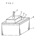
- Figure 14 is a perspective view showing a conventional semiconductor laser device disclosed in, for example "MITSUBISHI DENKI GIHO", Vol. 60, No.12, pp. 27 to 31, 1986.
- reference numeral 1 designates a heat sink formed of silver or diamond.
- a submount 2 formed of Si crystal is disposed on the heat sink 1.
- Gold gilding films 3 are formed on upper and lower surfaces of the submount 2.
- a semiconductor laser chip 6 is disposed on the submount 2.
- a p side electrode or an n side electrode 4 and an n side electrode or a p side electrode 5 are formed on lower and upper surfaces of the laser chip 6, respectively.
- the surface of the electrode 4 opposed to the submount 2 is plated with gold.
- a wire 7 is bonded to the electrode 5.
- the heat sink 1 is formed of metal and the laser chip 6 is formed of a semiconductor, there is a large difference between thermal expansion coefficients thereof.
- the thermal expansion coefficients of the heat sink and the laser chip are approximately 19.5 x 10 ⁇ 6 / °C and 6.5 X 10 ⁇ 6 / °C, respectively.
- the laser chip 6 is attached to the heat sink 1 using an appropriate soldering material at a high temperature.
- the submount 2 formed of Si crystal is inserted between the heat sink 1 and the laser chip 6 in the prior art. Since the thermal expansion coefficient of the Si crystal is relatively close to that of GaAs and the submount 2 formed of the Si crystal has an appropriate thickness (approximately 150 ⁇ m) the stress generated by the difference in thermal expansion coefficient is reduced because of the submount 2, so that the stress is not applied to the laser chip 6.
- Si crystal having a thickness of approximately 150 ⁇ m is inserted between the heat sink and the laser chip as a submount, a heat generated in the laser chip is hardly conducted. Therefore, it is not suitable for high output and high current injection operation.
- a wire has to be attached at a lower temperature in the future step and the wire is not reliably attached.
- the present invention is intended as a solution to the problems aforesaid.
- it is intended to provide a semiconductor device having a long life in which stress applied to a semiconductor element can be reduced and also heat generated by the semiconductor element can be reliably radiated.
- a semiconductor device comprising:
- the amorphous semiconductor film may, for example, be of amorphous silicon or of amorphous germanium.
- first and second metal films are disposed between the heat sink and the amorphous semiconductor film and between the amorphous semiconductor film and the semiconductor element, respectively, not only is the stress applied to the semiconductor element reduced but also good ohmic contact can be achieved by alloys formed between the amorphous semiconductor film and the first and second metal films.
- the metal films for example, may be of gold and gold-silicon or gold-germanium alloys may be formed. A high bonding strength and improved electrical conductivity can be achieved by this means.
- the amorphous semiconductor film may be restricted to a region which lies between the semiconductor element and the heat sink and a metal film of lower electrical resistance than the amorphous semiconductor film may be provided covering the amorphous semiconductor film and the adjacent surface of the heat sink.
- current flow and heat flow are differentiated and provide further reduction in stress, further reduction in thermal resistance and improved electrical conductivity.
- the amorphous semiconductor film can cover the major surface of the heat sink, and a metal film disposed is on the amorphous semiconductor film.
- An electrical wire can be bonded to this metal film and electrical current flow and heat flow can be differentiated as before.
- a method for manufacturing a semiconductor device having a function of radiating heat generated therein comprising the steps of:
- the semiconductor element is bonded to the heat sink whilst sintering and bonding operation is performed simultaneously. No high temperature is required for this processing and oxidation of the amorphous semiconductor film is avoided and the electrical characteristics are improved as a result.
- the amorphous semiconductor film may be of amorphous silicon or amorphous germanium and alloys may be formed between the amorphous semiconductor film and the first and second metal films.
- FIG. 1 is a perspective view showing a semiconductor laser as a semiconductor device in accordance with a first embodiment of the present invention.
- reference numeral 1 designates a heat sink formed of, for example silver.
- An amorphous semiconductor film 8 is arranged on the heat sink 1 and a semiconductor laser chip 6 is put on the heat sink 1 via the amorphous semiconductor film 8.
- Reference numeral 4 designates a p side electrode or an n side electrode of the semiconductor laser chip 6 and reference numeral 5 designates an n side electrode or p side electrode thereof.
- a wire 7 is bonded to the electrode 5.
- the heat sink 1 formed of, for example silver or diamond is prepared.
- the amorphous semiconductor film 8 is formed on the heat sink 1 by electron beam evaporation or sputtering.
- a temperature of the heatsink when the amorphous semiconductor film is formed is approximately 200°C.
- the semiconductor laser chip 6 having the electrodes 4 and 5 formed on both surfaces thereof is fixed onto the amorphous semiconductor film 8 using an appropriate soldering material.
- the wire 7 is bonded to the electrode 5 of the semiconductor laser chip 6 and then the semiconductor laser shown in figure 1 is completed.
- the amorphous semiconductor film 8 formed of, for example amorphous silicon is inserted between the heat sink 1 and the semiconductor laser chip 6.
- the heat sink and the semiconductor laser are bonded at a relatively high temperature of approximately 300 to 400°C and therefore, when the temperature falls to a room temperature, stress is applied to the semiconductor laser chip. Even when the semiconductor laser operates normally, heat is generated in the semiconductor laser chip. Since a thermal expansion coefficient of a crystal which constitutes the semiconductor laser chip is different from that of the heat sink, stress is applied to the semiconductor laser chip even during its operation. Thus, the semiconductor laser cannot operate for a long time.
- amorphous semiconductor used in the first embodiment of the present invention has various lattice constants unlike the crystal semiconductor.
- the semiconductor laser can operate for a long time.
- a Si crystal having a thickness of approximately 150 ⁇ m is used for reducing the stress, so that thermal resistance is considerably high.
- the amorphous semiconductor film in accordance with the first embodiment of the present invention has a function of effectively reducing stress even if it has a quite thin thickness of approximately 300 nm (3000 ⁇ ), with the result that the thermal resistance can be reduced.
- Figure 2(a) is a perspective view showing a semiconductor laser as a semiconductor device in accordance with a second embodiment of the present invention and figure 2(b) is an enlarged view showing a part of IIb in figure 2(a).
- a metal film 9 is formed on the heat sink 1 by gold gilding and amorphous silicon or amorphous germanium 8a is formed on the metal film 9.
- An alloy film 10 is formed between the amorphous silicon or amorphous germanium 8a and the metal film 9 and an alloy film 11 is formed between the amorphous silicon or amorphous germanium 8a and the p side electrode (or n side electrode) 4.
- Figures 3(a) to 3(e) are perspective views showing manufacturing steps for the semiconductor laser device in accordance with the second embodiment of the present invention.
- the heat sink 1 formed of, for example silver or diamond is prepared.
- the metal film 9 is formed on the heat sink 1 by gold gilding.
- the amorphous semiconductor film 8a formed of amorphous silicon or amorphous germanium is formed on the metal film 9 by electron beam evaporation or sputtering.
- the temperature of the heat sink 1 and metal film 9 when the amorphous semiconductor film is formed is approximately 200°C.
- the semiconductor laser chip 6 having the electrodes 5 and 4 formed on upper and bottom surfaces thereof, respectively, is put on the amorphous semiconductor film 8a and then heated up, while pressure or weight is applied from above. Then, the alloy films are formed between the amorphous semiconductor film 8a and the metal film 9 and the electrode 4, whereby the laser chip 6 is fixed onto the amorphous semiconductor film 8a without using a soldering material. Finally, referring to figure 3(e), the wire 7 is bonded to the electrode 5 of the semiconductor laser chip 6 and then the semiconductor laser is completed.
- the amorphous semiconductor film 8a formed of amorphous silicon or amorphous germanium is inserted between the semiconductor laser chip 6 and the heat sink 1 and the metal film 9 is provided on the heat sink.
- the alloy film 10 is formed at the bonding region.
- the alloy film 11 is formed between the electrode 4 of the semiconductor laser and the amorphous semiconductor film formed of amorphous silicon or amorphous germanium.
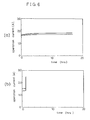
- Figure 6 shows data for describing effectiveness of the present invention.
- Figure 6(a) shows a result of an operation test of the semiconductor laser device when amorphous silicon having a thickness of approximately 300 nm (3000 ⁇ ), silver, and gold gilding film are used as the amorphous semiconductor film, the heat sink, and the metal film, respectively under conditions that an ambient temperature is 25°C and an optical output is 1W.
- Figure 6(b) shows an example when the silver heat sink is directly bonded to the semiconductor laser chip using a gold-silicon soldering material under the same conditions for comparison.
- the present invention stable operation can be continuously obtained for a long time.
- an optical output does not satisfy the operation condition because thermal resistance is too high.
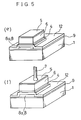
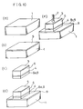
- Figure 4 is a perspective view showing a semiconductor laser as a semiconductor device in accordance with a third embodiment of the present invention.
- the same references as in figures 1 and 2 designate the same or corresponding parts.
- Reference numeral 12 designates an electrically conductive metal film provided on the amorphous semiconductor film 8 or 8a and the metal film 9.
- Figures 5(a) to 5(f) are perspective views showing manufacturing steps of the semiconductor laser in accordance with the third embodiment of the present invention.
- the heat sink 1 formed of, for example silver or diamond is prepared.
- the metal film 9 is formed on the heat sink 1 by, for example gold gilding.
- the amorphous semiconductor film is formed by electron beam evaporation or sputtering. Similar to the first and second embodiments of the present invention, when the amorphous semiconductor film is formed, the temperature of the heat sink 1 and metal film 9 is approximately 200°C. Then, the amorphous semiconductor film 8 or 8a is formed so as to be about the same size as that of the semiconductor laser chip by etching as shown in figure 5(c).
- the amorphous semiconductor film can be formed also by a lift-off method other than the above-described etching. According to this method, an oxide film or the like is formed on a part of the metal film 9 where the amorphous semiconductor film 8 or 8a is not to be formed before the amorphous semiconductor film is formed on the metal film 9 and then the amorphous semiconductor film is formed on the metal film 9 including a surface of the oxide film or the like by the same method as above and then an unnecessary part of the amorphous semiconductor film is removed by removing the oxide film or the like.
- the electrically conductive metal film 12 is formed on the amorphous semiconductor film 8 or 8a and the metal film 9 by resistive heating evaporation, electron beam evaporation, sputtering or gilding.
- the semiconductor laser chip 6 having the electrodes 5 and 4 formed on upper and bottom surfaces thereof, respectively, is put on the electrically conductive metal film 12 on the amorphous semiconductor film 8 or 8a with soldering material and then the assembly is heated up, while pressure is applied from above.
- the semiconductor laser chip 6 is fixed onto the metal film 12 and in a case where the amorphous semiconductor film 8a is formed of amorphous silicon or amorphous germanium, the alloy films are formed between the amorphous semiconductor film, the metal film 9 and the electrically conductive metal film 12.
- the gold wire 7 is bonded to the electrode 5 of the semiconductor laser chip 6 and then the semiconductor laser shown in figure 4 is completed.
- the electrically conductive metal film 12 is provided in order to divide a part where a current mainly flows from a part where a heat mainly flows.
- the amorphous semiconductor film is arranged only under the semiconductor laser and in the vicinity thereof, the semiconductor laser chip is prevented from receiving stress.
- the heat mainly flows through the amorphous semiconductor film the amorphous semiconductor film has a thin thickness of approximately 300 nm (3000 ⁇ ) as described above, so that thermal resistance is not increased.
- the electrically conductive metal film 12 and the metal film 9 have fairly high electric conductivity as compared with the amorphous semiconductor film, the current flows through the metal films 9 and 12, so that the electrical characteristic is in a good state.
- the metal film 9 is optional.
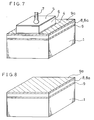
- Figure 7 is a perspective view showing a semiconductor laser as a semiconductor device in accordance with a fourth embodiment of the present invention.
- Reference numeral 9a designates a metal film provided on the amorphous semiconductor film. According to manufacturing steps of the semiconductor device in accordance with the fourth embodiment of the present invention, as shown in figure 8, the metal film 9, the amorphous semiconductor film 8 or 8a and the metal film 9a are formed on the heat sink 1 and then they are heated up once.
- the amorphous semiconductor film is not oxidized at all and also in a case where the amorphous semiconductor film 8a is formed of amorphous silicon or amorphous germanium, the alloy films are surely formed between the amorphous semiconductor film and the metal films 9 and 9a as shown in figure 9, which serves as ohmic contact. As a result, the electrical characteristic can be improved.
- Figure 10 are views showing a semiconductor laser as a semiconductor device and its manufacturing steps in accordance with a fifth embodiment of the present invention.
- the amorphous semiconductor film 8 or 8a is attached onto the semiconductor laser chip side during the manufacturing steps.
- the heat sink 1 is prepared.
- the metal film 9 is formed on the heat sink 1.
- the amorphous semiconductor film 8 (8a) is attached to a bottom surface of the semiconductor laser chip 6 having the electrodes 5 and 4 previously formed on upper and bottom surfaces thereof by electron beam evaporation or sputtering.
- the semiconductor laser chip formed as shown in figure 10(c) is put on the metal film 9 and then pressure or weight is applied from above,while the assembly is heated up.
- the alloy films are formed between the amorphous semiconductor film, the metal film 9 and the electrode 4, whereby the semiconductor laser chip is fixed onto the metal film 9.
- the laser chip can be fixed using an appropriate soldering material.
- strain caused by a difference between the thermal expansion coefficients of the heat sink 1 and the semiconductor laser chip 6 is reduced due to the amorphous semiconductor film 8 or 8a and even when the amorphous semiconductor film is very thin, it has an effect of reducing the strain, with the result that thermal resistance is not increased and the life of a laser element can be increased. Furthermore, since the alloy film is formed between the amorphous semiconductor film and the metal film, the electrical characteristic can be improved.
- Figure 11 is a view showing a laser chip of a semiconductor laser as a semiconductor device in accordance with a sixth embodiment of the present invention before it is attached to the heat sink.
- a metal film 9b is further formed just after the amorphous semiconductor film is formed on the semiconductor laser chip at the step shown in figure 10(c) in the fifth embodiment of the present invention.
- Figure 12 is a perspective view showing a semiconductor laser as a semiconductor device in accordance with a seventh embodiment of the present invention.
- the electrically conductive metal film 12 is formed on the whole surface of the amorphous semiconductor film and then a gild wire 7a is bonded to the metal film 12 to completely separate a current flow from a heat flow.
- a current flows as shown by an arrow of a solid line and a heat flows as shown by an arrow of a dotted line.
- any influence by the amorphous semiconductor film is not exerted on the electric conductivity.
- FIGS 13(a) to 13(f) are perspective views showing manufacturing steps for the semiconductor laser in accordance with a seventh embodiment of the present invention. Each step is described hereinafter with reference to the figure.
- the heat sink 1 is prepared.
- the metal film 9 is formed on the heat sink 1.
- the amorphous semiconductor film 8 or 8a is formed by electron beam evaporation or sputtering.
- the temperature of the heat sink 1 and metal film 9 is approximately 200°C.
- the electrically conductive metal film 12 is formed on the entire surface of the amorphous semiconductor film 8 or 8a by resistive heating evaporation, electron beam evaporation or sputtering. They can be heated up once in this state to form the alloy films between the amorphous semiconductor film 8 or 8a and the metal films 9 and 12.
- the semiconductor laser chip 6 having the electrodes 5 and 4 previously formed on upper and bottom surfaces thereof, respectively, is put on the electrically conductive metal film 12. Then, pressure or weight is applied from above, while the whole is heated up, so that the laser chip is fixed onto the metal film 12.
- the alloy films are formed between the amorphous semiconductor film 8 or 8a and the metal films 9 and 12 at the step shown in figure 13(e).
- the gold wires 7 and 7a are bonded to the electrode 5 of the semiconductor laser chip and the electrically conductive metal film 12.
- the semiconductor laser shown in figure 12 is completed.
- the present invention is not limited thereto. The same effect can be obtained even when the present invention is applied to any semiconductor device in which the semiconductor element is arranged on the heat sink and stress is generated when it is constructed or the element operates.
Landscapes
- Physics & Mathematics (AREA)
- Condensed Matter Physics & Semiconductors (AREA)
- General Physics & Mathematics (AREA)
- Electromagnetism (AREA)
- Optics & Photonics (AREA)
- Cooling Or The Like Of Semiconductors Or Solid State Devices (AREA)
- Semiconductor Lasers (AREA)
- Electrodes Of Semiconductors (AREA)
- Die Bonding (AREA)
Claims (16)
- Dispositif à semi-conducteur comprenant :un dissipateur thermique (1) pour rayonner de la chaleur; etun élément à semi-conducteur (6), d'un type produisant de la chaleur pendant son fonctionnement, monté sur une surface principale dudit dissipateur thermique (1);lequel dispositif à semi-conducteur est caractérisé par:un film semi-conducteur amorphe (8;8a) situé entre ledit dissipateur thermique (1) et ledit élément à semi-conducteur (6).
- Dissipateur à semi-conducteur, comme revendiqué en revendication 1, dans lequel :le film semi-conducteur amorphe précité (8a) est du silicium amorphe ou du germanium amorphe; etdes premier et second films métalliques (9,4) sont disposés entre le dissipateur thermique précité (1) et ledit film semi-conducteur amorphe (8a) et entre ledit film semi-conducteur amorphe (8a) et l'élément à semi-conducteur précité (6), respectivement, lesquels premier et second films métalliques (9,4) sont en contact ohmique avec ledit films semi-conducteur amorphe (8a) et produisent une liaison entre ledit film semi-conducteur amorphe (8a) et ledit dissipateur thermique (1) et ledit élément à semi-conducteur (6), respectivement.
- Dispositif à semi-conducteur selon la revendication 2 dans lequel des films d'alliage respectifs (10,11) sont formés entre le film semi-conducteur amorphe précité (8a) et le premier film métallique précité (9) et entre ledit film semi-conducteur amorphe (8a) et le second film métallique précité (4).
- Dispositif à semi-conducteur selon la revendication 3 dans lequel le second film métallique précité (4) est un film de dorure d'or formé sur le film semi-conducteur amorphe précité (8a).
- Dispositif à semi-conducteur selon la revendication 3, dans lequel le second film métallique précité (4) est un film de dorure d'or formé sur une surface d'une électrode de l'élément à semi-conducteur précité (6) au côté en contact avec le film semi-conducteur amorphe précité (8a).
- Dispositif à semi-conducteur, comme revendiqué en revendication 1, dans lequel :le film semi-conducteur amorphe précité (8a) est situé seulement sur une région de la surface principale du dissipateur thermique précité (1) où l'élément à semi-conducteur (6) précité est monté; etun film métallique (12) de résistance électrique plus faible que celle dudit film à semi-conducteur amorphe (8a) est disposé sur ledit film semi-conducteur amorphe (8a) et le restant de la surface principale dudit dissipateur thermique (1).
- Dispositif à semi-conducteur, comme revendiqué en revendication 1, dans lequel :le film semi-conducteur amorphe précité (8a) recouvre la surface principale du dissipateur thermique précité (1); etun film métallique (9a;12) est disposé sur ledit film semi-conducteur amorphe (8a).
- Dispositif à semi-conducteur comme revendiqué dans l'une ou l'autre des revendications 6 ou 7, dans lequel le film métallique précité (12;9a) est un film de dorure d'or.
- Dispositif à semi-conducteur comme revendiqué en revendidication 7 comprenant un fil d'alimentation en courant (7a) directement lié au film métallique précité (12).
- Dispositif à semi-conducteur comme revendiqué dans l'une quelconque des revendications précédentes, dans lequel le film semi-conducteur amorphe précité est d'une épaisseur de 300 nm (3000 Å).
- Procédé pour fabriquer un dispositif à semi-conducteur ayant une fonction de rayonnement de chaleur produite dans celui-ci, comprenant les étapes de :former un premier film métallique (9) sur un dissipateur thermique (1) pour rayonner de la chaleur;former un film semi-conducteur amorphe (8,8a) sur ledit premier film métallique (9) et ensuite former un second film métallique (9a) sur ledit film semi-conducteur amorphe (8,8a);placer un élément à semi-conducteur (6) sur ledit second film métallique (9a); etsollicier ledit élément à semi-conducteur (6) et ledit second film métallique (9a) ensemble et chauffer en même temps pour lier ledit élément à semi-conducteur (6) audit dissipateur thermique (1).
- Procédé comme revendiqué en revendication 11, dans lequel des films d'alliage respectifs (10,11) sont formés entre le film semi-conducteur amorphe précité (8,8a) et les premier et second films métalliques précités (9,9a).
- Procédé pour fabriquer un dispositif à semi-conducteur selon l'une ou l'autre des revendications 11 ou 12, dans lequel le film semi-conducteur amorphe précité (8,8a) est formé de silicium amorphe ou de germanium amorphe.
- Procédé pour fabriquer un dispositif à semi-conducteur selon la revendication 13, dans lequel le film semi-conducteur amorphe précité (8,8a) est formé par évaporation de faisceau d'électrons ou pulvérisation.
- Procédé pour fabriquer un dispositif à semi-conducteur selon la revendication 14, dans lequel la température du dissipateur thermique (1) et du premier film métallique (9) est de 200°C lorsque le film semi-conducteur amorphe précité (8,8a) est formé.
- Procédé pour fabriquer un dispositif à semi-conducteur comme revendiqué en revendication 13, dans lequel le second film métallique précité (9a) est un film de dorure d'or formé sur une surface d'une électrode de l'élément à semi-conducteur précité (6) faisant face au film semi-conducteur amorphe précité (8,8a).
Applications Claiming Priority (2)
| Application Number | Priority Date | Filing Date | Title |
|---|---|---|---|
| JP2147761A JP2726141B2 (ja) | 1990-06-05 | 1990-06-05 | 半導体装置およびその製造方法 |
| JP147761/90 | 1990-06-05 |
Publications (2)
| Publication Number | Publication Date |
|---|---|
| EP0460785A1 EP0460785A1 (fr) | 1991-12-11 |
| EP0460785B1 true EP0460785B1 (fr) | 1996-04-17 |
Family
ID=15437570
Family Applications (1)
| Application Number | Title | Priority Date | Filing Date |
|---|---|---|---|
| EP91300584A Expired - Lifetime EP0460785B1 (fr) | 1990-06-05 | 1991-01-25 | Dispositif semi-conducteur comprenant un refroidisseur |
Country Status (4)
| Country | Link |
|---|---|
| US (2) | US5247203A (fr) |
| EP (1) | EP0460785B1 (fr) |
| JP (1) | JP2726141B2 (fr) |
| DE (1) | DE69118750T2 (fr) |
Families Citing this family (16)
| Publication number | Priority date | Publication date | Assignee | Title |
|---|---|---|---|---|
| JPH04293287A (ja) * | 1991-03-22 | 1992-10-16 | Sanyo Electric Co Ltd | 半導体レーザ装置 |
| SG59997A1 (en) * | 1995-06-07 | 1999-02-22 | Ibm | Apparatus and process for improved die adhesion to organic chip carries |
| US5792677A (en) * | 1997-01-16 | 1998-08-11 | Ford Motor Company | Embedded metal planes for thermal management |
| US6084775A (en) * | 1998-12-09 | 2000-07-04 | International Business Machines Corporation | Heatsink and package structures with fusible release layer |
| JP3429213B2 (ja) | 1999-02-26 | 2003-07-22 | シャープ株式会社 | 集積回路 |
| US6273322B1 (en) * | 1999-05-12 | 2001-08-14 | Aichi Steel Corporation | Productive method of amorphous metal-metal jointed parts and amorphous metal-metal jointed parts |
| US6486499B1 (en) * | 1999-12-22 | 2002-11-26 | Lumileds Lighting U.S., Llc | III-nitride light-emitting device with increased light generating capability |
| JP4514376B2 (ja) * | 2001-09-27 | 2010-07-28 | シャープ株式会社 | 窒化物半導体レーザ装置 |
| US6449158B1 (en) * | 2001-12-20 | 2002-09-10 | Motorola, Inc. | Method and apparatus for securing an electronic power device to a heat spreader |
| US6749105B2 (en) * | 2002-03-21 | 2004-06-15 | Motorola, Inc. | Method and apparatus for securing a metallic substrate to a metallic housing |
| JP4430112B2 (ja) * | 2007-03-28 | 2010-03-10 | 古河電気工業株式会社 | 熱伝導膜、熱伝導膜を備える半導体デバイスおよび電子機器 |
| US7816155B2 (en) * | 2007-07-06 | 2010-10-19 | Jds Uniphase Corporation | Mounted semiconductor device and a method for making the same |
| EP2769408A1 (fr) * | 2011-10-20 | 2014-08-27 | Crucible Intellectual Property, LLC | Dissipateur de chaleur en alliage amorphe en vrac |
| JP6116413B2 (ja) * | 2013-07-09 | 2017-04-19 | 三菱電機株式会社 | 電力用半導体装置の製造方法 |
| JP6912716B2 (ja) * | 2017-08-10 | 2021-08-04 | 富士通株式会社 | 半導体装置及びその製造方法 |
| DE102018101453A1 (de) * | 2018-01-23 | 2019-07-25 | Borgwarner Ludwigsburg Gmbh | Heizvorrichtung und Verfahren zum Herstellung eines Heizstabes |
Family Cites Families (8)
| Publication number | Priority date | Publication date | Assignee | Title |
|---|---|---|---|---|
| US4698662A (en) * | 1985-02-05 | 1987-10-06 | Gould Inc. | Multichip thin film module |
| JPS628641U (fr) * | 1985-06-28 | 1987-01-19 | ||
| GB2194388A (en) * | 1986-08-20 | 1988-03-02 | Plessey Co Plc | Integrated circuit devices |
| EP0304337B1 (fr) * | 1987-08-20 | 1994-10-05 | Canon Kabushiki Kaisha | Substrat hybride |
| JP2539878B2 (ja) * | 1988-02-12 | 1996-10-02 | 三菱電機株式会社 | レ―ザプリンタ用半導体レ―ザ装置の駆動方法 |
| JPH0750813B2 (ja) * | 1988-05-23 | 1995-05-31 | 三菱電機株式会社 | 半導体レーザ素子用サブマウント |
| US4861426A (en) * | 1989-01-23 | 1989-08-29 | The United States Of America As Represented By The Secretary Of The Army | Method of making a millimeter wave monolithic integrated circuit |
| US5031029A (en) * | 1990-04-04 | 1991-07-09 | International Business Machines Corporation | Copper device and use thereof with semiconductor devices |
-
1990
- 1990-06-05 JP JP2147761A patent/JP2726141B2/ja not_active Expired - Lifetime
-
1991
- 1991-01-25 EP EP91300584A patent/EP0460785B1/fr not_active Expired - Lifetime
- 1991-01-25 DE DE69118750T patent/DE69118750T2/de not_active Expired - Fee Related
- 1991-02-01 US US07/649,062 patent/US5247203A/en not_active Expired - Fee Related
-
1993
- 1993-05-24 US US08/065,761 patent/US5332695A/en not_active Expired - Fee Related
Also Published As
| Publication number | Publication date |
|---|---|
| JPH0439956A (ja) | 1992-02-10 |
| JP2726141B2 (ja) | 1998-03-11 |
| DE69118750D1 (de) | 1996-05-23 |
| DE69118750T2 (de) | 1996-09-05 |
| EP0460785A1 (fr) | 1991-12-11 |
| US5332695A (en) | 1994-07-26 |
| US5247203A (en) | 1993-09-21 |
Similar Documents
| Publication | Publication Date | Title |
|---|---|---|
| JP3271475B2 (ja) | 電気素子の接合材料および接合方法 | |
| EP0460785B1 (fr) | Dispositif semi-conducteur comprenant un refroidisseur | |
| KR100913762B1 (ko) | 금속-세라믹 복합 기판 및 그 제조 방법 | |
| US7518155B2 (en) | Light emitting element mounting member, and semiconductor device using the same | |
| KR100940164B1 (ko) | 서브마운트 및 반도체 장치 | |
| EP0606522B1 (fr) | Dispositif semi-conducteur et procécé de fabrication et de montage de dispositifs semi-conducteurs | |
| US5217922A (en) | Method for forming a silicide layer and barrier layer on a semiconductor device rear surface | |
| US6664640B2 (en) | Semiconductor device | |
| US7030496B2 (en) | Semiconductor device having aluminum and metal electrodes and method for manufacturing the same | |
| KR20050061452A (ko) | 서브 마운트 및 반도체 장치 | |
| JPH08203924A (ja) | 半導体装置 | |
| JPH0722435A (ja) | 半導体装置およびその製造方法 | |
| JP3767585B2 (ja) | 半導体装置 | |
| US5311399A (en) | High power ceramic microelectronic package | |
| EP1939929B1 (fr) | Dissipateur thermique utilisant une couche de brasure et procédé de fabrication d'un tel dissipateur thermique | |
| CA1153128A (fr) | Circuits electriques | |
| JPS61181136A (ja) | ダイボンデイング方法 | |
| JPH0671105B2 (ja) | 磁電変換素子の製造方法 | |
| JPH0728095B2 (ja) | 半導体発光装置 | |
| JPS5966182A (ja) | 半導体装置の製造方法 | |
| JPH02304940A (ja) | 半導体装置の製造方法 |
Legal Events
| Date | Code | Title | Description |
|---|---|---|---|
| PUAI | Public reference made under article 153(3) epc to a published international application that has entered the european phase |
Free format text: ORIGINAL CODE: 0009012 |
|
| AK | Designated contracting states |
Kind code of ref document: A1 Designated state(s): DE FR GB |
|
| 17P | Request for examination filed |
Effective date: 19911216 |
|
| 17Q | First examination report despatched |
Effective date: 19940328 |
|
| GRAH | Despatch of communication of intention to grant a patent |
Free format text: ORIGINAL CODE: EPIDOS IGRA |
|
| GRAA | (expected) grant |
Free format text: ORIGINAL CODE: 0009210 |
|
| AK | Designated contracting states |
Kind code of ref document: B1 Designated state(s): DE FR GB |
|
| REF | Corresponds to: |
Ref document number: 69118750 Country of ref document: DE Date of ref document: 19960523 |
|
| ET | Fr: translation filed | ||
| PLBE | No opposition filed within time limit |
Free format text: ORIGINAL CODE: 0009261 |
|
| STAA | Information on the status of an ep patent application or granted ep patent |
Free format text: STATUS: NO OPPOSITION FILED WITHIN TIME LIMIT |
|
| 26N | No opposition filed | ||
| PGFP | Annual fee paid to national office [announced via postgrant information from national office to epo] |
Ref country code: DE Payment date: 19991231 Year of fee payment: 10 |
|
| PGFP | Annual fee paid to national office [announced via postgrant information from national office to epo] |
Ref country code: FR Payment date: 20000112 Year of fee payment: 10 |
|
| PGFP | Annual fee paid to national office [announced via postgrant information from national office to epo] |
Ref country code: GB Payment date: 20000119 Year of fee payment: 10 |
|
| PG25 | Lapsed in a contracting state [announced via postgrant information from national office to epo] |
Ref country code: GB Free format text: LAPSE BECAUSE OF NON-PAYMENT OF DUE FEES Effective date: 20010125 |
|
| GBPC | Gb: european patent ceased through non-payment of renewal fee |
Effective date: 20010125 |
|
| PG25 | Lapsed in a contracting state [announced via postgrant information from national office to epo] |
Ref country code: FR Free format text: LAPSE BECAUSE OF NON-PAYMENT OF DUE FEES Effective date: 20010928 |
|
| PG25 | Lapsed in a contracting state [announced via postgrant information from national office to epo] |
Ref country code: DE Free format text: LAPSE BECAUSE OF NON-PAYMENT OF DUE FEES Effective date: 20011101 |
|
| REG | Reference to a national code |
Ref country code: FR Ref legal event code: ST |