EP0460835A2 - Wiedereinrichtung einer Synchron-Digital-Multiplexhierarchie - Google Patents
Wiedereinrichtung einer Synchron-Digital-Multiplexhierarchie Download PDFInfo
- Publication number
- EP0460835A2 EP0460835A2 EP91304709A EP91304709A EP0460835A2 EP 0460835 A2 EP0460835 A2 EP 0460835A2 EP 91304709 A EP91304709 A EP 91304709A EP 91304709 A EP91304709 A EP 91304709A EP 0460835 A2 EP0460835 A2 EP 0460835A2
- Authority
- EP
- European Patent Office
- Prior art keywords
- pointer
- node
- data stream
- timing
- line
- Prior art date
- Legal status (The legal status is an assumption and is not a legal conclusion. Google has not performed a legal analysis and makes no representation as to the accuracy of the status listed.)
- Granted
Links
Images

Classifications
-
- H—ELECTRICITY
- H04—ELECTRIC COMMUNICATION TECHNIQUE
- H04J—MULTIPLEX COMMUNICATION
- H04J3/00—Time-division multiplex systems
- H04J3/02—Details
- H04J3/06—Synchronising arrangements
- H04J3/0635—Clock or time synchronisation in a network
- H04J3/0685—Clock or time synchronisation in a node; Intranode synchronisation
-
- H—ELECTRICITY
- H04—ELECTRIC COMMUNICATION TECHNIQUE
- H04L—TRANSMISSION OF DIGITAL INFORMATION, e.g. TELEGRAPHIC COMMUNICATION
- H04L7/00—Arrangements for synchronising receiver with transmitter
-
- H—ELECTRICITY
- H04—ELECTRIC COMMUNICATION TECHNIQUE
- H04J—MULTIPLEX COMMUNICATION
- H04J3/00—Time-division multiplex systems
- H04J3/02—Details
- H04J3/06—Synchronising arrangements
- H04J3/062—Synchronisation of signals having the same nominal but fluctuating bit rates, e.g. using buffers
- H04J3/0623—Synchronous multiplexing systems, e.g. synchronous digital hierarchy/synchronous optical network (SDH/SONET), synchronisation with a pointer process
Definitions
- the present invention concerns the digital transmission of data and in particular data transmitted by what is known as SDH (Synchronous Digital Hierarchy).
- SDH Synchronous Digital Hierarchy
- time division multiplexing was used to combine the serial bit streams of four such systems into one bit stream for more economical transmission. This became known as second-order digital multiplexing.
- third, fourth and fifth-order multiplexers have led to third, fourth and fifth-order multiplexers, as progressively more streams are combined. These have traditionally been used in a hierarchy to assemble telephony, data or other traffic to the highest bit rate possible for economic transmission.
- Next data is read out from all the stores in parallel by a common read-out clock known as the carrier clock.
- the read-out or carrier clock is arranged to be faster than the fastest expected input clock.
- a pulse is occasionally removed from the read clock for each individual tributary so that no data bit is read out of the store. Instead a dummy bit is transmitted which will be removed by the multiplexer at the receive end of the transmission path. This is known as positive justification.
- Positive/zero/negative justification is the justification technique which has been proposed for SDH.
- SDH when the network is synchronous or appears to be synchronous for a period, then no justification may appear for some considerable period. Figures of more than one second are possible as are figure of more than a whole day.
- the justification process is controlled by what is called a data pointer and the utilisation of the data pointer for this purpose is called pointer processing.
- pointer processing When justification does occur 8 more bits or 8 less bits will be sent in a given period. The effect of this is that when a final 2084 kbit/s tributary output is generated which has had either positive or negative justification a phase jump of nearly 4 microseconds will occur.
- the invention also comprises apparatus for carrying out the aforesaid method.
- the best known European synchronous Muldex is that used to assemble 30 speech channels into a PCM (Pulse Code Modulation) signal at 2 Mbit/s.
- the frame structure is defined in CCITT recommendation G704. All of the channels use the same 2 Mbit/s clock for their encoding processes.
- the key features of the system include basic modules which are synchronous to each other. Each basic module has spaces left in the frame structure for later addition of transmission support services and for the addition of multiplexer overheads. The modules are based on a time period of 125 microseconds. This allows cross connection down to 64 kbit/s if suitable frame stores are added.
- Pointer bytes are associated with the start of a multiplexer frame. These pointer bytes show where, within a frame, can be found the Reference Word (the frame alignment word or the beginning of a block of traffic within the frame). As the clock associated with the traffic drifts so the pointer changes value.
- FIG. 1 shows a part of a typical muldex.
- Incoming data lines are shown at 1, 1a ... 1n which terminate at SDH line terminators 2, 2a ... 2n respectively.
- Each of the terminators 2 ... 2n is connected to a triplicated switch core 4, 4a, 4b.
- each of the incoming lines will have a rate determined by its line reference which may be different from that of the switch although ideally the line and switch references should be identical.
- Figure 1 is merely one example of a node in an SDH transmission network. In general terms each incoming data stream will have its line reference and a node will have a node reference.
- Section A of Figure 1 is an expanded diagram of SDH line terminator 2n and it will be appreciated that the other terminators are identical to it.
- the incoming and outgoing lines 1n, 3n are terminated by an optical interface 5, the incoming line is rejustified by a Rejustifer circuit 6 connected to a Triplication/Discrepancy Checker 7 connected to the three identical sections of the switch core 4a, 4b and 4c.
- the line terminator also includes a control circuit 8 controlled by a processor (not shown). Apart from the details of the Rejustifier Circuit 6, which will be described later, this arrangement is entirely conventional.
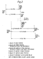
- Figure 2 of the drawings shows a Line reference. This is the 8 kH z reference that is multiplied up to give the 155.52 MH z Line Clock and also the 19.44 MH z Line byte clock. It can be considered as occurring when the first byte, out of 270, of the first row out of nine of a frame arrives at the line interface.
- STM-1 Section Overheads
- the Data Pointer is a value, in Figure 2 (r ), from which the position of the Reference word in the frame can be calculated.
- the value r of the pointer can be decremented every time a VC4 word is received as it is written into the buffer.
- the address to which each word is written is determined from the decremented value of the pointer.
- the Line Reference has a period of 125 microseconds which is defined by the time between its successive 8 KH z reference markers.
- the Data pointer As defined by the current SDH standard, has 783 possible values.
- the Data Line Reference occurs at approximately the time that the Reference word is received by the rejustifier from the line.
- the Reference Word is the first word, sometimes byte, of the VC4 that the Data Pointer refers to. Consequently the Reference Word can always be written to location zero of the buffer.
- a Read Buffer Address counter (full range of 783) is used to address the buffer to extract words for the VC4 payload. As each word is extracted the counter is decremented.
- the Switch Preference is the equivalent in the switch to the Line Preference, and it is dealing with possible phase drift between the Line and Switch Reference that this invention is concerned.
- the Switch Reference is the 8 KH z reference which is multiplied up to give the 155.52 MH z Switch Output Bit Clock and the more usable 19.44 MH z Switch byte clock.
- the Switch Reference can be considered as occurring when the first byte (out of 270) of the first row (out of 9) of the regenerated SDH stream leaves the rejustifier interface.
- the Data Switch Reference is the 8 kH2 reference that occurs at approximately the time the Reference Byte leaves the rejustifier.
- the pointer As defined by the current SDH standard, has 783 possible values. If the value of this Data pointer is R then the Data Line Reference occurs R X 125/783 microseconds after the Switch Reference.
- the H3 and V3 bytes are of course used during justification, but even at peak justification rates only 25% of the V3 bytes can be used for justification.
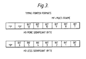
- the most significant bit of the H3 or V3 byte will be an indicator to say if the remaining bits form the lower significiant 7 bits of the timing pointer, or the upper significant 6 bits.
- Timing Pointer For a VC4 payload the Timing Pointer, which is not defined by the current SDH standard, has 6480 possible values. If the value of this Timing Pointer is g then the Timing Reference occurs (g x 125/6480) microseconds after the Timing Line Reference. In a manner similar to the Data pointer the Timing pointer is defined by a value, in the present description g which is extracted from the SOH and validated.
- the value (g) of the pointer can be decremented every 19.29 ns until it reaches zero.
- the start of the decrement corresponds to the Line Reference.
- the time the decrement reaches zero corresponds to the Timing Line Reference.
- This "state change" is sampled by a switch 51.84 MH z clock. Consequently a sampling error of up to 19.29 ns can result.
- This "state change” is used to freeze the value (g′) of a counter which starts counting from zero at the time of the Switch Reference. This now gives a Timing Line Reference related to the Switch Reference.
- Timing Switch Reference can be generated which is a constant (C) number of 19.29 ns later than the Timing Line Reference.
- the Timing Switch Pointer (G) is generated by adding C to the frozen value (g′) on the counter.
- Timing Switch Reference has therefore been derived from the Timing Line Reference with a maximum of + 19.29 ns of phase distortion caused by the sampling error.
- the regenerated Timing Switch Pointer can then be continually re-inserted into the outgoing VC4 H3 byte.
- FIG. 3 of the drawings shows typical timing pointer formats.
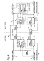
- FIG. 4 of the drawings this is a block diagram showing an embodiment of utilising the Data and Timing pointers just described and corresponding to Justifier Circuit 6 of Figure 1.
- the input data stream is shown at 10 along with the Line Reference at 11 and 51.84 MH z Clock at 12.
- the input data stream is written into a data buffer 13, whilst the Data Pointer is extracted in a Data Pointer Extractor circuit 14 under the control of the Line Reference 11 and Line Clock 12.
- the Timing Pointer is supplied to a Timing Reference Generator 15 to which the Line Reference 11 and Line Clock 12 are also fed.
- the output of Timing Reference Generator 15 is supplied to a Timing Transfer circuit 16 connected the 51.84 MH z Switch Clock 17
- Timing Transfer circuit 16 The output from the Timing Transfer circuit 16 is connected to a Timing Pointer generator 18 which is supplied with the 8 KH z Switch Reference 17 and the 51. 84 MH z Switch Clock 19.
- the Switch Clock 17 and the Switch Reference 19 are both supplied to a Read Address and Data Pointer generator 20 which provides Read Addresses for the data buffer 13 to generate an output data stream 21.
- the Read Data Pointer and the Switch Timing Pointer are compared by a comparator and justification control circuit 22 and discrepancies between the two pointers are indicated to the Read Address and Data Pointer generator 20 which corrects the Switch Data Pointer value by justification.
- Timing Switch Pointer By mathematically converting the Timing Switch Pointer to an equivalent Date Switch Pointer and comparing this equivalent with the actual Data Switch Pointer used to read the Data bytes from the Data buffer 13, decisions can be made as to whether the actual Data Switch Pointer is at the correct value or not.
- the actual Data Switch Pointer can be adjusted by performing either the appropriate positive or negative justification sequences, or for gross errors, such as at power on, the new Pointer Indication sequence. These sequences are already defined by the SDH recommendations.
- timing pointer is only giving an indication of the phase reference of the payload, the occasional missing timing pointer because of a negative justification or corruption of the pointer field is not critical.
- the mechanism of only normally permitting one (or two) increment (or decrement) at a time will allow a simple filtering method to ignore received timing pointers which have been corrupted.
- timing pointers it is possible to limit the phase distortion induced at a pointer processing node to 19.29 nanoseconds.
- the pointer processing will cause significant phase distortion.
- a timing pointer will be transmitted onto the next pointer processing node, only 19.29 nanoseconds of phase distortion will occur at the next node provided the incoming timing pointer is used.
- desynchronisers When timing pointers are not used, desynchronisers will produce more than the 1.5 UI permitted by G.823 and the 2 UI permitted by G. 824.
- Bit leaking is not an acceptable method because it introduces phase distortions and creates wander. When equipment does not receive timing pointers bit leaking will be used and the user of the equipment must accept the phase distortions that result.
Landscapes
- Engineering & Computer Science (AREA)
- Computer Networks & Wireless Communication (AREA)
- Signal Processing (AREA)
- Computer Hardware Design (AREA)
- Time-Division Multiplex Systems (AREA)
- Synchronisation In Digital Transmission Systems (AREA)
- Data Exchanges In Wide-Area Networks (AREA)
Applications Claiming Priority (2)
| Application Number | Priority Date | Filing Date | Title |
|---|---|---|---|
| GB909012436A GB9012436D0 (en) | 1990-06-04 | 1990-06-04 | Sdh rejustification |
| GB9012436 | 1990-06-04 |
Publications (3)
| Publication Number | Publication Date |
|---|---|
| EP0460835A2 true EP0460835A2 (de) | 1991-12-11 |
| EP0460835A3 EP0460835A3 (en) | 1993-03-03 |
| EP0460835B1 EP0460835B1 (de) | 1997-12-29 |
Family
ID=10677043
Family Applications (1)
| Application Number | Title | Priority Date | Filing Date |
|---|---|---|---|
| EP91304709A Expired - Lifetime EP0460835B1 (de) | 1990-06-04 | 1991-05-24 | Wiedereinrichtung einer Synchron-Digital-Multiplexhierarchie |
Country Status (13)
| Country | Link |
|---|---|
| US (1) | US5172376A (de) |
| EP (1) | EP0460835B1 (de) |
| JP (1) | JPH04261239A (de) |
| KR (1) | KR920001886A (de) |
| CN (1) | CN1059437A (de) |
| AU (1) | AU7818891A (de) |
| CA (1) | CA2043375A1 (de) |
| DE (1) | DE69128498T2 (de) |
| ES (1) | ES2110430T3 (de) |
| FI (1) | FI912651A7 (de) |
| GB (2) | GB9012436D0 (de) |
| IE (1) | IE911772A1 (de) |
| PT (1) | PT97850A (de) |
Cited By (9)
| Publication number | Priority date | Publication date | Assignee | Title |
|---|---|---|---|---|
| EP0525770A3 (en) * | 1991-07-31 | 1993-08-04 | Nec Corporation | Method and apparatus for renewing au-4 and tu-3 pointers of synchronous digital hierarchy |
| WO1993022856A1 (en) * | 1992-04-23 | 1993-11-11 | Nokia Telecommunications Oy | Synchronization of sdh signals |
| US5386419A (en) * | 1992-08-20 | 1995-01-31 | U.S. Philips Corporation | Multiplexer for at least two independently operating signal sources |
| EP0620663A3 (en) * | 1993-04-14 | 1995-08-16 | Plessey Telecomm | Method for synchronisation of digital data transmission. |
| EP0674407A3 (de) * | 1994-03-23 | 1996-01-31 | Plessey Telecomm | Komplementäre Justierung. |
| WO1996039761A1 (en) * | 1995-06-06 | 1996-12-12 | Symmetricom, Inc. | Encoding system for distribution of synchronization |
| US5828670A (en) * | 1995-06-06 | 1998-10-27 | Symmetricom, Inc. | Distribution of synchronization in a synchronous optical environment |
| EP0782082A3 (de) * | 1995-12-27 | 1999-06-09 | Nec Corporation | Vorrichtung zur seriellen Datenübertragung |
| EP1494377A1 (de) * | 2003-07-01 | 2005-01-05 | Nortel Networks Limited | Digitale Verarbeitung von Sonetanzeigern |
Families Citing this family (34)
| Publication number | Priority date | Publication date | Assignee | Title |
|---|---|---|---|---|
| DE4013317A1 (de) * | 1990-04-26 | 1990-08-23 | Ant Nachrichtentech | Stopfverfahren zur reduktion des wartezeitjitters und anordnung zur durchfuehrung des verfahrens |
| DE69220128T2 (de) * | 1991-03-28 | 1997-09-18 | Nippon Electric Co | Empfangssystem in einer synchrones Endstation |
| JPH05183530A (ja) * | 1991-06-06 | 1993-07-23 | Fujitsu Ltd | 同期ペイロードポインタ処理方式 |
| JP2725486B2 (ja) * | 1991-06-28 | 1998-03-11 | 日本電気株式会社 | ポインタ処理回路 |
| FI89757C (fi) * | 1991-10-08 | 1993-11-10 | Nokia Telecommunications Oy | Foerfarande foer att utfoera en anslutningsutjaemning |
| US5717693A (en) * | 1992-05-21 | 1998-02-10 | Alcatel Network Systems, Inc. | Sonet payload pointer processing and architecture |
| AU665072B2 (en) | 1992-05-21 | 1995-12-14 | Alcatel N.V. | TDM synchronous state machine |
| US5379277A (en) * | 1992-06-17 | 1995-01-03 | Nec Corporation | Path monitoring bit extraction device |
| EP0578315A1 (de) * | 1992-07-09 | 1994-01-12 | Philips Patentverwaltung GmbH | Synchrones Übertragungssystem |
| DE4238899A1 (de) * | 1992-11-19 | 1994-05-26 | Philips Patentverwaltung | Übertragungssystem der synchronen digitalen Hierarchie |
| GB2275852B (en) * | 1993-03-05 | 1997-02-26 | Sony Broadcast & Communication | Signal synchroniser with resynchronise control |
| JPH06268625A (ja) * | 1993-03-12 | 1994-09-22 | Matsushita Electric Ind Co Ltd | ディジタル信号伝送方法および送受信装置および伝送装 置 |
| JP3168487B2 (ja) * | 1993-03-15 | 2001-05-21 | 富士通株式会社 | 同期確立チェック方法及び伝送装置 |
| FI93288C (fi) * | 1993-03-16 | 1995-03-10 | Nokia Telecommunications Oy | Menetelmä ehdollisten kytkentöjen ohjaamiseksi tietoliikennejärjestelmässä |
| FI93287C (fi) * | 1993-03-16 | 1995-03-10 | Nokia Telecommunications Oy | Menetelmä toisiinsa kytkettyjen SDH- ja PDH-tietoliikenneverkkojen synkronoimiseksi |
| FI93289C (fi) * | 1993-03-16 | 1995-03-10 | Nokia Telecommunications Oy | Menetelmä ehdollisten kytkentöjen ohjaamiseksi synkronisessa digitaalisessa tietoliikennejärjestelmässä |
| FI94812C (fi) * | 1993-05-18 | 1995-10-25 | Nokia Telecommunications Oy | Menetelmä ja laite tasauspäätöksen aikaansaamiseksi synkronisen digitaalisen tietoliikennejärjestelmän solmupisteessä |
| EP0645914A1 (de) * | 1993-09-20 | 1995-03-29 | ALCATEL BELL Naamloze Vennootschap | Knotenpunkt für Telekommunicationsnetz |
| GB9323187D0 (en) * | 1993-11-10 | 1994-01-05 | Northern Telecom Ltd | Pointer justification even leak control |
| US5883900A (en) * | 1994-03-23 | 1999-03-16 | Gpt Limited | Telecommunications transmission |
| DE4437136A1 (de) * | 1994-10-18 | 1996-04-25 | Philips Patentverwaltung | Übertragungssystem mit einem Regelkreis |
| US5781597A (en) * | 1995-02-16 | 1998-07-14 | Alcatel Sel Aktiengesellschaft | Synchronous digital transmission system having justification circuit that counts frame bytes, calculates offsets, compares thresholds, and initiates justification action |
| GB9509216D0 (en) * | 1995-05-05 | 1995-06-28 | Plessey Telecomm | Retiming arrangement for SDH data transmission system |
| US5563890A (en) * | 1995-06-14 | 1996-10-08 | National Semiconductor Corporation | SONET/SDH pointer justification gap elimination circuit |
| US5761203A (en) * | 1996-04-04 | 1998-06-02 | Lucent Technologies Inc. | Synchronous and asynchronous recovery of signals in an ATM network |
| GB2358764B (en) * | 2000-01-28 | 2004-06-30 | Vegastream Ltd | Casualty-based memory access ordering in a multriprocessing environment |
| US6738395B1 (en) * | 2000-09-15 | 2004-05-18 | Nortel Networks Limited | Pointer processing and path BIP-8 computation for large concatenated payloads |
| DE10064988A1 (de) * | 2000-12-23 | 2002-06-27 | Alcatel Sa | Netzwerkeinrichtung und Verfahren zur Laufzeitkompensation von Datenpaketen |
| KR20030014077A (ko) * | 2001-08-10 | 2003-02-15 | 최승국 | 판별 경계치 변조 방식의 포인터 조정 동기 장치 |
| US7353288B1 (en) * | 2001-10-17 | 2008-04-01 | Ciena Corporation | SONET/SDH payload re-mapping and cross-connect |
| AU2002321955A1 (en) * | 2002-09-06 | 2004-03-29 | Telefonaktiebolaget Lm Ericsson (Publ) | Switching arrangement including time-slot buses and several buffers |
| US7606269B1 (en) * | 2004-07-27 | 2009-10-20 | Intel Corporation | Method and apparatus for detecting and managing loss of alignment in a virtually concatenated group |
| CN1859052B (zh) * | 2005-12-29 | 2011-06-15 | 华为技术有限公司 | 一种异步时钟域信号处理方法及系统 |
| KR102622775B1 (ko) * | 2022-11-22 | 2024-01-09 | 주식회사 오성전자 | 리모컨에서 피제어기기 등록 방법 및 이를 지원하는 시스템 |
Family Cites Families (6)
| Publication number | Priority date | Publication date | Assignee | Title |
|---|---|---|---|---|
| JPS4943809B1 (de) * | 1968-10-25 | 1974-11-25 | ||
| US3646271A (en) * | 1970-04-24 | 1972-02-29 | Nippon Electric Co | Pcm retiming method |
| JPS6214546A (ja) * | 1985-07-12 | 1987-01-23 | Nec Corp | 準同期バツフア制御方式 |
| CA1262173A (en) * | 1986-05-29 | 1989-10-03 | James Angus Mceachern | Synchronization of asynchronous data signals |
| EP0396669B1 (de) * | 1988-10-14 | 1995-06-28 | Digital Equipment Corporation | Verfahren und anordnung zur wahrnehmung bevorstehender überläufe und/oder unterschreitungen eines elastischen puffers |
| US5113395A (en) * | 1989-09-14 | 1992-05-12 | Nec Corporation | Frame phase aligning system using a buffer memory with a reduced capacity |
-
1990
- 1990-06-04 GB GB909012436A patent/GB9012436D0/en active Pending
-
1991
- 1991-05-23 IE IE177291A patent/IE911772A1/en unknown
- 1991-05-24 DE DE69128498T patent/DE69128498T2/de not_active Expired - Fee Related
- 1991-05-24 ES ES91304709T patent/ES2110430T3/es not_active Expired - Lifetime
- 1991-05-24 EP EP91304709A patent/EP0460835B1/de not_active Expired - Lifetime
- 1991-05-24 GB GB9111235A patent/GB2249002B/en not_active Expired - Fee Related
- 1991-05-29 US US07/706,989 patent/US5172376A/en not_active Expired - Fee Related
- 1991-06-03 JP JP3160032A patent/JPH04261239A/ja active Pending
- 1991-06-03 CA CA002043375A patent/CA2043375A1/en not_active Abandoned
- 1991-06-03 FI FI912651A patent/FI912651A7/fi not_active Application Discontinuation
- 1991-06-03 KR KR1019910009177A patent/KR920001886A/ko not_active Withdrawn
- 1991-06-04 AU AU78188/91A patent/AU7818891A/en not_active Abandoned
- 1991-06-04 PT PT97850A patent/PT97850A/pt not_active Application Discontinuation
- 1991-06-04 CN CN91104363A patent/CN1059437A/zh active Pending
Cited By (14)
| Publication number | Priority date | Publication date | Assignee | Title |
|---|---|---|---|---|
| EP0525770A3 (en) * | 1991-07-31 | 1993-08-04 | Nec Corporation | Method and apparatus for renewing au-4 and tu-3 pointers of synchronous digital hierarchy |
| WO1993022856A1 (en) * | 1992-04-23 | 1993-11-11 | Nokia Telecommunications Oy | Synchronization of sdh signals |
| US5386419A (en) * | 1992-08-20 | 1995-01-31 | U.S. Philips Corporation | Multiplexer for at least two independently operating signal sources |
| EP0620663A3 (en) * | 1993-04-14 | 1995-08-16 | Plessey Telecomm | Method for synchronisation of digital data transmission. |
| US5544172A (en) * | 1993-04-14 | 1996-08-06 | Gpt Limited | Method for the digital transmission of data |
| EP0674407A3 (de) * | 1994-03-23 | 1996-01-31 | Plessey Telecomm | Komplementäre Justierung. |
| WO1996039761A1 (en) * | 1995-06-06 | 1996-12-12 | Symmetricom, Inc. | Encoding system for distribution of synchronization |
| US5638379A (en) * | 1995-06-06 | 1997-06-10 | Symmetricom, Inc. | Encoding system for distribution of synchronization |
| US5828670A (en) * | 1995-06-06 | 1998-10-27 | Symmetricom, Inc. | Distribution of synchronization in a synchronous optical environment |
| EP0782082A3 (de) * | 1995-12-27 | 1999-06-09 | Nec Corporation | Vorrichtung zur seriellen Datenübertragung |
| EP1494377A1 (de) * | 2003-07-01 | 2005-01-05 | Nortel Networks Limited | Digitale Verarbeitung von Sonetanzeigern |
| US7369578B2 (en) | 2003-07-01 | 2008-05-06 | Nortel Networks Limited | Digital processing of SONET pointers |
| EP2124364A3 (de) * | 2003-07-01 | 2010-10-27 | Nortel Networks Limited | Digitale Verarbeitung von Sonetanzeigern |
| EP2124365A3 (de) * | 2003-07-01 | 2010-10-27 | Nortel Networks Limited | Digitale Verarbeitung von Sonetanzeigern |
Also Published As
| Publication number | Publication date |
|---|---|
| DE69128498T2 (de) | 1998-04-16 |
| PT97850A (pt) | 1993-06-30 |
| GB9012436D0 (en) | 1990-07-25 |
| GB2249002A (en) | 1992-04-22 |
| FI912651A0 (fi) | 1991-06-03 |
| KR920001886A (ko) | 1992-01-30 |
| EP0460835A3 (en) | 1993-03-03 |
| GB2249002B (en) | 1994-07-13 |
| EP0460835B1 (de) | 1997-12-29 |
| US5172376A (en) | 1992-12-15 |
| CN1059437A (zh) | 1992-03-11 |
| CA2043375A1 (en) | 1991-12-05 |
| ES2110430T3 (es) | 1998-02-16 |
| JPH04261239A (ja) | 1992-09-17 |
| GB9111235D0 (en) | 1991-07-17 |
| IE911772A1 (en) | 1991-12-04 |
| FI912651A7 (fi) | 1991-12-05 |
| DE69128498D1 (de) | 1998-02-05 |
| AU7818891A (en) | 1991-12-05 |
Similar Documents
| Publication | Publication Date | Title |
|---|---|---|
| US5172376A (en) | Sdh rejustification | |
| CA1232693A (en) | Network multiplex structure | |
| EP0788695B1 (de) | Verfahren zum zerlegen und zusammensetzen von rahmenstrukturen mit zeigern | |
| US5065396A (en) | Inverse multiplexer and demultiplexer techniques | |
| US7830909B2 (en) | Transparent sub-wavelength network | |
| JPH0767099B2 (ja) | デイジタル広帯域信号の伝送方法 | |
| EP0788694B1 (de) | Verfahren und einrichtung zur elastischen pufferung in einem synchronen digitalen fernmeldesystem | |
| JP3656140B2 (ja) | Sdhデータ伝送システムのリタイミング構造 | |
| FI90484C (fi) | Menetelmä ja laite synkronisessa digitaalisessa tietoliikennejärjestelmässä käytettävän elastisen puskurimuistin täyttöasteen valvomiseksi | |
| EP1537694B1 (de) | Synchroner übertragungsnetzknoten | |
| US7016344B1 (en) | Time slot interchanging of time slots from multiple SONET signals without first passing the signals through pointer processors to synchronize them to a common clock | |
| JPH0761056B2 (ja) | 特定フレーム構造体への情報ビットの挿入装置 | |
| JP3356032B2 (ja) | 多重化伝送装置、ポインタ処理装置、多重化伝送網および多重化伝送装置の構成方法 | |
| KR0152724B1 (ko) | E1-ds3 다중/역다중 장치 | |
| JPH06188867A (ja) | ディジタル信号通信方式 | |
| HK1002380B (en) | Method for disassembling and assembling frame structures containing pointers | |
| HK1002378B (en) | Method and equipment for elastic buffering in a synchronous digital telecommunication system | |
| HK1011805B (en) | Method and equipment for monitoring the fill rate of an elastic buffer memory in a synchronous digital telecommunication system |
Legal Events
| Date | Code | Title | Description |
|---|---|---|---|
| PUAI | Public reference made under article 153(3) epc to a published international application that has entered the european phase |
Free format text: ORIGINAL CODE: 0009012 |
|
| AK | Designated contracting states |
Kind code of ref document: A2 Designated state(s): BE DE DK ES FR GR IT LU NL SE |
|
| PUAL | Search report despatched |
Free format text: ORIGINAL CODE: 0009013 |
|
| AK | Designated contracting states |
Kind code of ref document: A3 Designated state(s): BE DE DK ES FR GR IT LU NL SE |
|
| 17P | Request for examination filed |
Effective date: 19930824 |
|
| 17Q | First examination report despatched |
Effective date: 19951027 |
|
| GRAG | Despatch of communication of intention to grant |
Free format text: ORIGINAL CODE: EPIDOS AGRA |
|
| GRAG | Despatch of communication of intention to grant |
Free format text: ORIGINAL CODE: EPIDOS AGRA |
|
| GRAH | Despatch of communication of intention to grant a patent |
Free format text: ORIGINAL CODE: EPIDOS IGRA |
|
| GRAH | Despatch of communication of intention to grant a patent |
Free format text: ORIGINAL CODE: EPIDOS IGRA |
|
| GRAA | (expected) grant |
Free format text: ORIGINAL CODE: 0009210 |
|
| AK | Designated contracting states |
Kind code of ref document: B1 Designated state(s): BE DE DK ES FR GR IT LU NL SE |
|
| PG25 | Lapsed in a contracting state [announced via postgrant information from national office to epo] |
Ref country code: GR Free format text: LAPSE BECAUSE OF FAILURE TO SUBMIT A TRANSLATION OF THE DESCRIPTION OR TO PAY THE FEE WITHIN THE PRESCRIBED TIME-LIMIT Effective date: 19971229 Ref country code: DK Free format text: LAPSE BECAUSE OF NON-PAYMENT OF DUE FEES Effective date: 19971229 |
|
| ITF | It: translation for a ep patent filed | ||
| ET | Fr: translation filed | ||
| REF | Corresponds to: |
Ref document number: 69128498 Country of ref document: DE Date of ref document: 19980205 |
|
| REG | Reference to a national code |
Ref country code: ES Ref legal event code: FG2A Ref document number: 2110430 Country of ref document: ES Kind code of ref document: T3 |
|
| PG25 | Lapsed in a contracting state [announced via postgrant information from national office to epo] |
Ref country code: SE Free format text: LAPSE BECAUSE OF FAILURE TO SUBMIT A TRANSLATION OF THE DESCRIPTION OR TO PAY THE FEE WITHIN THE PRESCRIBED TIME-LIMIT Effective date: 19980329 |
|
| PGFP | Annual fee paid to national office [announced via postgrant information from national office to epo] |
Ref country code: FR Payment date: 19980511 Year of fee payment: 8 |
|
| PG25 | Lapsed in a contracting state [announced via postgrant information from national office to epo] |
Ref country code: LU Free format text: LAPSE BECAUSE OF NON-PAYMENT OF DUE FEES Effective date: 19980524 |
|
| PGFP | Annual fee paid to national office [announced via postgrant information from national office to epo] |
Ref country code: ES Payment date: 19980526 Year of fee payment: 8 |
|
| PGFP | Annual fee paid to national office [announced via postgrant information from national office to epo] |
Ref country code: DE Payment date: 19980529 Year of fee payment: 8 |
|
| PGFP | Annual fee paid to national office [announced via postgrant information from national office to epo] |
Ref country code: NL Payment date: 19980531 Year of fee payment: 8 |
|
| PGFP | Annual fee paid to national office [announced via postgrant information from national office to epo] |
Ref country code: BE Payment date: 19980714 Year of fee payment: 8 |
|
| PLBE | No opposition filed within time limit |
Free format text: ORIGINAL CODE: 0009261 |
|
| STAA | Information on the status of an ep patent application or granted ep patent |
Free format text: STATUS: NO OPPOSITION FILED WITHIN TIME LIMIT |
|
| 26N | No opposition filed | ||
| PG25 | Lapsed in a contracting state [announced via postgrant information from national office to epo] |
Ref country code: ES Free format text: THE PATENT HAS BEEN ANNULLED BY A DECISION OF A NATIONAL AUTHORITY Effective date: 19990525 |
|
| PG25 | Lapsed in a contracting state [announced via postgrant information from national office to epo] |
Ref country code: BE Free format text: LAPSE BECAUSE OF NON-PAYMENT OF DUE FEES Effective date: 19990531 |
|
| BERE | Be: lapsed |
Owner name: GPT LTD Effective date: 19990531 |
|
| PG25 | Lapsed in a contracting state [announced via postgrant information from national office to epo] |
Ref country code: NL Free format text: LAPSE BECAUSE OF NON-PAYMENT OF DUE FEES Effective date: 19991201 |
|
| PG25 | Lapsed in a contracting state [announced via postgrant information from national office to epo] |
Ref country code: FR Free format text: LAPSE BECAUSE OF NON-PAYMENT OF DUE FEES Effective date: 20000131 |
|
| NLV4 | Nl: lapsed or anulled due to non-payment of the annual fee |
Effective date: 19991201 |
|
| PG25 | Lapsed in a contracting state [announced via postgrant information from national office to epo] |
Ref country code: DE Free format text: LAPSE BECAUSE OF NON-PAYMENT OF DUE FEES Effective date: 20000301 |
|
| REG | Reference to a national code |
Ref country code: FR Ref legal event code: ST |
|
| REG | Reference to a national code |
Ref country code: ES Ref legal event code: FD2A Effective date: 20020204 |
|
| PG25 | Lapsed in a contracting state [announced via postgrant information from national office to epo] |
Ref country code: IT Free format text: LAPSE BECAUSE OF NON-PAYMENT OF DUE FEES;WARNING: LAPSES OF ITALIAN PATENTS WITH EFFECTIVE DATE BEFORE 2007 MAY HAVE OCCURRED AT ANY TIME BEFORE 2007. THE CORRECT EFFECTIVE DATE MAY BE DIFFERENT FROM THE ONE RECORDED. Effective date: 20050524 |