EP0460840A2 - Digitalfehlerkorrektursystem für in Bereiche unterteilten Analog-Digitalwandler - Google Patents
Digitalfehlerkorrektursystem für in Bereiche unterteilten Analog-Digitalwandler Download PDFInfo
- Publication number
- EP0460840A2 EP0460840A2 EP91304721A EP91304721A EP0460840A2 EP 0460840 A2 EP0460840 A2 EP 0460840A2 EP 91304721 A EP91304721 A EP 91304721A EP 91304721 A EP91304721 A EP 91304721A EP 0460840 A2 EP0460840 A2 EP 0460840A2
- Authority
- EP
- European Patent Office
- Prior art keywords
- analog
- signal
- binary
- stage
- conversion
- Prior art date
- Legal status (The legal status is an assumption and is not a legal conclusion. Google has not performed a legal analysis and makes no representation as to the accuracy of the status listed.)
- Withdrawn
Links
Images


Classifications
-
- H—ELECTRICITY
- H03—ELECTRONIC CIRCUITRY
- H03M—CODING; DECODING; CODE CONVERSION IN GENERAL
- H03M1/00—Analogue/digital conversion; Digital/analogue conversion
- H03M1/06—Continuously compensating for, or preventing, undesired influence of physical parameters
-
- H—ELECTRICITY
- H03—ELECTRONIC CIRCUITRY
- H03M—CODING; DECODING; CODE CONVERSION IN GENERAL
- H03M1/00—Analogue/digital conversion; Digital/analogue conversion
- H03M1/10—Calibration or testing
- H03M1/1009—Calibration
- H03M1/1033—Calibration over the full range of the converter, e.g. for correcting differential non-linearity
- H03M1/1057—Calibration over the full range of the converter, e.g. for correcting differential non-linearity by trimming, i.e. by individually adjusting at least part of the quantisation value generators or stages to their nominal values
- H03M1/1061—Calibration over the full range of the converter, e.g. for correcting differential non-linearity by trimming, i.e. by individually adjusting at least part of the quantisation value generators or stages to their nominal values using digitally programmable trimming circuits
-
- H—ELECTRICITY
- H03—ELECTRONIC CIRCUITRY
- H03M—CODING; DECODING; CODE CONVERSION IN GENERAL
- H03M1/00—Analogue/digital conversion; Digital/analogue conversion
- H03M1/10—Calibration or testing
- H03M1/1009—Calibration
- H03M1/1033—Calibration over the full range of the converter, e.g. for correcting differential non-linearity
- H03M1/1038—Calibration over the full range of the converter, e.g. for correcting differential non-linearity by storing corrected or correction values in one or more digital look-up tables
- H03M1/1042—Calibration over the full range of the converter, e.g. for correcting differential non-linearity by storing corrected or correction values in one or more digital look-up tables the look-up table containing corrected values for replacing the original digital values
-
- H—ELECTRICITY
- H03—ELECTRONIC CIRCUITRY
- H03M—CODING; DECODING; CODE CONVERSION IN GENERAL
- H03M1/00—Analogue/digital conversion; Digital/analogue conversion
- H03M1/12—Analogue/digital converters
- H03M1/14—Conversion in steps with each step involving the same or a different conversion means and delivering more than one bit
- H03M1/16—Conversion in steps with each step involving the same or a different conversion means and delivering more than one bit with scale factor modification, i.e. by changing the amplification between the steps
- H03M1/164—Conversion in steps with each step involving the same or a different conversion means and delivering more than one bit with scale factor modification, i.e. by changing the amplification between the steps the steps being performed sequentially in series-connected stages
- H03M1/167—Conversion in steps with each step involving the same or a different conversion means and delivering more than one bit with scale factor modification, i.e. by changing the amplification between the steps the steps being performed sequentially in series-connected stages all stages comprising simultaneous converters
Definitions
- the present invention generally relates to multi-stage, pipelined subranging analog-to-digital converters and, more particularly, to a system for correcting conversion errors in multi-stage pipelined, subranging analog-to-digital converters.
- a subranging analog-to-digital converter is described by A.G.F. Dingwall and W. Zazzu in "An 8-MHz CMOS Subranging 8-Bit A/D Converter", IEEE J. Solid-State Circuits , Vol. SC-20, pp. 1138-1143, December 1985, and S.H. Lewis and P.R. Gray in "A Pipelined 5-M Sample/s 9-Bit Analog-To-Digital Converter", IEEE J. Solid-State Circuits , Vol. SC-22, No. 6, pp. 954-961, December 1987.
- the interstage gain is made one half of the conventional amount, i.e., 2 L-1 for a stage that uses L-bit analog-to-digital (A/D) and digital-to-analog (D/A) converters.
- the residual signal thus spans only half of the range of the subsequent stage.
- errors in the A/D converter of any stage up to ⁇ 1/2 of a least significant bit (LSB), can be accommodated.
- LSB least significant bit
- Such errors will cause the amplified residual signal to fall either above or below the expected range and can be corrected by either incrementing or decrementing the L-bit A/D converter code for the prior stage respectively.
- this method is very simple, it cannot correct any error in the D/A converter, or in the gain stage, and it is not sufficient for high resolution (i.e., resolution above 9 bits).
- Subranging analog-to-digital converters are attractive for high-speed operation since they are almost comparable in speed to a flash converter, but use far less hardware.
- an N-bit flash converter makes use of 2 N - 1 comparators, while the same resolution in an L stage subranging architecture requires only L(2 N/L -1) comparators.
- efforts to obtain high resolution are hampered by practical circuit nonidealities such as component mismatching, nonlinearity, offset, noise, etc.
- accuracy is limited by the degree of linearity of the A/D and D/A converters in the first stage. Resolution at accuracy levels beyond the limits of the nonideal components mentioned above, however, is obtainable by use of this invention.
- a digital error correction system facilitates calibration of the subranging analog-to-digital converter to avoid errors in the operation of the converter. High resolution analog-to-digital conversion with a subranging architecture is thereby facilitated.
- the intent is to use digital techniques as much as possible to mitigate the effects of component mismatches and nonlinearities that otherwise limit resolution to a lower level.
- the architecture which supports a digitally correctable A/D converter is consistent with general subranging architectures so as to be efficient in terms of required chip area and power dissipation.
- the architecture is also amenable to pipelining for high-speed operation, and uses a limited number of digital coefficients to implement the correction of the circuit nonidealities.
- Application of that approach is intended to enable analog-to-digital conversion to take place with accuracy levels considerably beyond the limits imposed by circuit nonidealities or impairments. It is contemplated that 16-bit resolution at conversion rates of upwards of 25 MHz, well beyond the present state of the art, can be obtained from standard integrated circuit technologies using the present invention.
- the converter includes a plurality of conversion stages connected in cascade, each stage including a sample-and-hold circuit, an analog-to-digital converter for converting an analog input signal into a binary conversion signal which corresponds to the nearest quantized level below that of the analog input signal, a digital-to-analog converter for converting the binary conversion signal into a quantized analog signal which corresponds to the nearest quantized level below that of the analog input signal, summation means for subtracting the quantized analog signal from the analog,input signal to generate a residual analog signal, and a gain amplifier which amplifies the residual analog signal for application to the next conversion stage.
- the binary conversion signal addresses an individual look-up table to provide a compensated binary signal which is selected to compensate for nonidealities of the converter components.
- the compensated binary signals from the look-up tables provide a corrected output signal when combined or summed together.
- the binary conversion signal in the stages for the most significant bits address a common look-up table, while each of the remaining stages addresses a respective individual look-up table.
- a simple method of calibration which makes use of a least-mean-squared adaptation algorithm, is also provided.
- This technique accommodates practical circuit nonidealities such as component mismatching, gain error and voltage offsets, and also handles high levels of amplifier nonlinearity.
- the architecture is applicable to any subranging converter with an arbitrary number of stages and number of bits per stage.
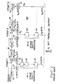
- FIG. 1 A block diagram of a basic subranging converter, as known in the prior art, is shown in Figure 1.
- the converter comprises two or more similar conversion stages (1, 2,...M) connected together in a cascade arrangement.
- Each conversion stage includes a sample-and-hold (S/H) circuit 10 to which an analog input signal is applied.
- S/H sample-and-hold
- Each stage uses a low resolution A/D converter 12 to generate a binary conversion signal corresponding to the nearest quantized level below that of the analog input signal applied to sample-and-hold circuit 10 of that stage, while a companion D/A converter 14 generates a quantized analog signal corresponding to the nearest quantized level below that of the analog input signal applied to the sample-and-hold circuit 10 of that stage.
- This quantized analog signal in each stage is subtracted from the analog input signal in that stage by a summation circuit 16 which generates a residual analog signal that is less than one LSB of the digital-to-analog converter 14 in that stage.
- a subsequent gain amplifier 18 in each stage boosts the residual signal in that stage back to a level consistent with the input range of the next stage.
- each stage digitally approximates its analog input signal and passes the remainder of that analog signal (after amplification) on to the following stage for further processing.
- each stage In pipelined operation, the signal processed by each stage is delayed from the preceding stage by one sample period. Thus a latency of M clock cycles is required before an output signal is available from the final stage.
- the output signals of earlier stages are available sooner and must be delayed accordingly before being combined into a single output signal.
- This is implemented, as shown in Figure 1, by advancing the binary conversion signal from the analog-to-digital converter 12 of each conversion stage through a plurality of stages 20 of a shift register in each conversion stage.
- the shift register in each successive conversion stage has one less stage 20 than the shift register of the previous conversion stage, except for the final conversion stage which employs no shift register.
- the parallel outputs from each conversion stage are combined to produce a resultant binary output signal which represents the analog input signal to the multi-stage analog-to-digital converter.
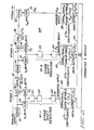
- the architecture of multi-stage analog-to-digital converter 64 shown in Figure 2, is an improvement of the subranging architecture of Figure 1 discussed above.
- the improved architecture comprises the basic pipelined subranging structure of Figure 1 along with individual digital look-up tables 30 for each of the conversion stages (1, 2,...M).
- the M sets of uncorrected digital output signals D i , 1 ⁇ i ⁇ M, of the M subranging stages address the respective M look-up tables 30.
- each look-up table 30 implements an arbitrary discrete valued nonlinear function of its digital input signal. A method to calibrate the converter, i. e., to incorporate the required coefficients into the look-up tables, is described below.
- Each look-up table 30 can be constructed as either a read only memory (ROM) or a random access memory (RAM), depending on the desired calibration method.
- Each look-up table 30 has a number of binary address inputs equal to the number of bits of the A/D converter 12 for its respective stage, i.e., n i binary address inputs for any stage i in Figure 2, and thus have 2 n i coefficients.
- the binary word size of these coefficients, in any stage is greater than the total number of bits of A/D converter 12 in that stage, to facilitate correction and calibration.
- the interstage amplifiers 18 have gains of less than what is required for a conventional subranging analog-to-digital converter.
- the gains of the gain amplifiers 18 and sample-and-hold circuits 10 are reduced to accommodate errors in the interstage A/D and D/A converters, i.e., G i ⁇ 2 i n ; 1 ⁇ i ⁇ M
- G i ⁇ 2 i n A practical choice of gain is that used in the digital correct ion method G i ⁇ 2 i-1 n ; 1 ⁇ i ⁇ M
- the actual gain values chosen could be greater or less than these amounts, depending on the expected values of errors.
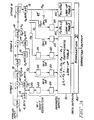
- FIG. 3 A variation 64′ of the pipelined multi-stage analog-to-digital converter is shown in Figure 3 wherein like reference numerals indicate the same (or corresponding) elements as in Figure 2.
- a single look-up table 31 is used for the most significant bits (MSBs) corresponding to D L output signals of the first L stages.
- MSBs most significant bits
- Separate look-up tables 30′ are used for each of the remaining stages.
- the required number of coefficients in this implementation increases to It is desirable to keep the number of stages L connected to the first look-up table 31 as small as possible to minimize the number of coefficients.
- the A/D converter implementation 64′ of Figure 3 uses a larger total number of digital coefficients to enable it to correct more accurately for errors due to static nonlinearities.
- the number of stages L incorporated together as inputs to the first table in A/D converter 64′ governs the degree of nonlinearity that is correctable therein. In general, the smallest number of stages that provides acceptable nonlinearity correction should be used in order to reduce the total number of table coefficients required. Nonlinearity in subsequent stages L+1 to M are not corrected; however, their effects are attenuated by their input-referred gains as mentioned earlier.
- Calibration can be done in various ways depending on the application. For example, a general approach that uses a least-mean-squared (LMS) adaptive algorithm is described by B. Widrow and S.D. Stearns in Adaptive Signal Processing , Prentice-Hall, 1985, pp. 99-114. Two examples, shown in Figures 4A and 4B, use an ideal (in relation to the specific application), so-called “gold standard”, converter to generate what is termed an "exact” output and use LMS adaptation of the look-up table coefficients. In actual practice, the "gold-standard", or reference, converter needs to be only one order of magnitude (or less) better in accuracy than the objective specification for the analog-to-digital converter after calibration.
- LMS least-mean-squared
- a 14-bit "gold-standard” converter is adequate.
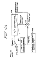
- the techniques shown in Figures 4A and 4B differ only in that a digital-to-analog converter 40 is used as the "gold standard" reference in Figure 4A whereas an analog-to-digital converter 50 is used in Figure 4B.
- the use of the D/A converter standard is probably the most practical approach to implement since it is usually easier to make a high precision D/A converter than an A/D converter.
- the table look-up LMS algorithm is for the A/D converter 64 of Figure 2 and for the A/D converter 64′ of Figure 3, where ⁇ n is the error after the n th iteration, and ⁇ is the convergence coefficient, usually a constant, and normally ⁇ 1.
- Table F1(D1, D2...D L ) designates a memory block with an output selected by the concatenation of address bits D1 through D L .
- the word size of the table coefficients should be greater than the desired number of bits to allow for ⁇ I. In this algorithm, only the coefficient from each table that was used in forming the n th output is updated at each iteration. Speed of adaptation therefore drops with respect to the size of tables that are used, i.e., the more coefficients per table, the longer it takes to converge since only one coefficient per table is adjusted on each conversion. Other adaptation algorithms may be used if appropriate.
- a random sequence generator 48 applies a random binary signal to an ideal ("gold standard") digital-to-analog converter 40.
- the binary signal is converted into an analog signal which is applied via a switch S1 to the input of the multi-stage analog-to-digital converter 64.
- a digital subtractor 52 computes the difference between the binary signal from random sequence generator 48 and the binary output signal produced by summation unit 32 (shown in Figures 2 and 3) and produces an error signal ⁇ representing the difference between the binary signals.
- the error signal ⁇ is applied to a processor (not shown) which performs an adaptation algorithm and returns a corrected coefficient to each of the look-up tables of multi-stage analog-to-digital converter 64.
- a random signal generator 60 applies a random analog signal via a switch S1 to an ideal ("gold standard") analog-to-digital converter 50 and to the input of multi-stage analog-to-digital converter 64.
- a digital subtractor 62 computes the difference between the binary signal produced by the "gold standard” analog-to-digital converter 50 and the binary output signal from summation unit 32 (shown in Figures 2 and 3) and produces an error signal ⁇ representing the difference between the binary signals.
- the error signal ⁇ is applied to a processor (not shown) which performs an adaptation algorithm and returns a corrected coefficient to each of the look-up tables of multi-stage analog-to-digital converter 64. It should be noted that the foregoing description of operation of the system of Figure 4B is the same if analog-to-digital converter 64′ (of Figure 3) is substituted for analog-to-digital converter 64 (of Figure 2).
- the A/D converters of the improved architecture operate properly and correct errors for high accuracy.
- the A/D converters can be calibrated during manufacture and the coefficients can be stored in the correction memory of the A/D converters for later use.
- the A/D converter itself does not require calibration hardware, thereby avoiding this complexity and the costs associated therewith, and consists only of the circuitry shown in either Figure 2 or Figure 3.
- a system for calibrating either of these embodiments of the A/D converter during manufacture, or in applications requiring recalibration is shown in Figure 5.
- the system includes the A/D converter 64 to be calibrated (although A/D converter 64′, shown in Figure 3, may be used instead) along with an external "gold-standard" reference A/D or D/A converter, external look-up tables (or memory blocks) and a processor.
- the external coefficients can be programmed into a programmable ROM (PROM) or electronically erasable PROM (EEPROM) on the A/D converter chip itself.
- PROM 30 is shown in the calibration system (or calibration fixture) of Figure 5.
- the memory within the off-chip hardware converges to a calibrated set of coefficient values using the update algorithm, i.e., the table look-up LMS algorithm described earlier.
- the advantage of using this technique is that the on-chip circuitry for calibration is kept to a minimum. In environments where substantial changes in circuit operating conditions due to variations in power supply levels or temperature could put a corrected A/D converter out of specification, the calibration circuitry of Figures 4(a), 4(b) or 5 must be included along with the A/D converter to permit periodic recalibration.
- multi-stage analog-to-digital converter 64 (though analog-to-digital converter 64′ may be used in the same way instead) is placed in a calibration fixture which includes a random sequence generator 70 for supplying a random binary signal to a "gold standard" digital-to-analog converter 72 wherein the binary signal is converted into an analog signal.
- the output analog signal from D/A converter 72 is applied via a switch S1 to the analog input of multi-stage analog-to-digital converter 64.
- the uncorrected output signals from each stage of the multi-stage analog-to-digital converter are applied to a set of external look-up tables 74 which correspond to look-up tables 30 in the conversion stages of multi-stage analog-to-digital converter 64.
- the external look-up tables 74 produce binary signals or coefficients which are combined by a summation unit 76 to produce a binary output signal.
- a digital subtractor 78 computes the difference between the binary signal generated by random sequence generator 70 and the binary output signal from summation unit 76 and produces an error signal ⁇ representing the difference between the latter two binary signals. Error signal ⁇ is applied to a processor 80, or to a finite state machine (not shown), which performs an update algorithm to correct the coefficients in look-up tables 74 until error signal ⁇ is reduced to a level close to zero.
- the coefficients stored in external look-up tables 74 are stored in the internal look-up tables 30 of multi-stage analog-to-digital converter 64.
- the calibration fixture of Figure 5 can employ a random analog signal generator and a "gold standard" analog-to-digital converter arranged as shown in Figure 4B for calibration of multi-stage analog-to-digital converter 64.
- analog-to-digital converter 64′ shown in Figure 3, may be used in the calibration system of Figure 5 in the same manner as analog-to-digital converter 64.
- the calibration circuitry can alternatively be incorporated on-chip.
- An oversampled D/A or A/D converter operated at a reduced conversion rate or other high precision D/A or A/D converter can be used as the "gold standard" reference.
- Other variations in implementation are possible and within the scope of this invention, including a configuration whereby the correction coefficients are stored externally and loaded into internal RAM after calibration.
- Another configuration within the scope of this invention employs a separate digital system or chip to implement the correction using PROM or RAM along with a processor or a finite state machine.
- This invention also encompasses discrete (i.e., circuit board level) implementations, in addition to the integrated circuit oriented approaches described herein.
- the logic of the calibration process is shown in the flow chart of Figure 6 for the A/D converter 64 of Figure 2.
- the process described is for the calibration system illustrated in Figure 4A.
- the process starts by resetting an n register in multi-stage A/D converter 64 at step 90. This is a register that keeps track of the number of calibration cycles performed.
- a voltage V in is then generated by first inputting a random number to "gold standard" D/A converter 40 from random sequence generator 48 at step 92, and this random number is supplied by D/A converter 40 to A/D converter 64 at step 94.
- the analog-to-digital process is initiated at step 96.
- the 1 register is set to 1 at step 106.
- the error ⁇ in the converted output signal is determined as the difference between V in and V A/D by subtractor 52 (shown in Figure 4A) or subtractor 78 (shown in Figure 5).
- the corrected coefficient for the 1 th table is generated at step 110 as the sum of the output signal of the 1 th table for an input address of D1 and a change in the error, ⁇ , and the 1 register is then incremented by one at step 112. This process continues until 1 is greater than n stages , the number of stages of the pipelined A/D converter, as determined at step 114. At this point, the n register is incremented by one at step 116.
- a test is next made at step 118 to determine if the content of the n register is greater than the number of calibration cycles. If not, the process loops back to step 92 and the process repeats. When the n register content exceeds the number of calibration cycles, the calibration process is complete.
- the A/D converter is being calibrated. If calibration is being performed during manufacture using external hardware, as shown in Figure 5, then the calibration coefficients must subsequently be programmed into the internal look-up tables of the A/D converter 64 (or 64′). If the calibration hardware is incorporated in a system together with the A/D converter itself, then the next step is to transfer coefficients to internal A/D converter look-up tables if external tables were used. Once this is done, in either situation, the A/D converter is ready for normal signal conversion operation.
Landscapes
- Engineering & Computer Science (AREA)
- Theoretical Computer Science (AREA)
- Physics & Mathematics (AREA)
- Nonlinear Science (AREA)
- Analogue/Digital Conversion (AREA)
Applications Claiming Priority (2)
| Application Number | Priority Date | Filing Date | Title |
|---|---|---|---|
| US07/533,263 US5047772A (en) | 1990-06-04 | 1990-06-04 | Digital error correction system for subranging analog-to-digital converters |
| US533263 | 1990-06-04 |
Publications (2)
| Publication Number | Publication Date |
|---|---|
| EP0460840A2 true EP0460840A2 (de) | 1991-12-11 |
| EP0460840A3 EP0460840A3 (en) | 1993-10-20 |
Family
ID=24125199
Family Applications (1)
| Application Number | Title | Priority Date | Filing Date |
|---|---|---|---|
| EP19910304721 Withdrawn EP0460840A3 (en) | 1990-06-04 | 1991-05-24 | Digital error correction system for subranging analog-to-digital converters |
Country Status (7)
| Country | Link |
|---|---|
| US (1) | US5047772A (de) |
| EP (1) | EP0460840A3 (de) |
| JP (1) | JPH0583134A (de) |
| KR (1) | KR940005935B1 (de) |
| CN (1) | CN1057136A (de) |
| CA (1) | CA2042142A1 (de) |
| IL (1) | IL98220A0 (de) |
Cited By (8)
| Publication number | Priority date | Publication date | Assignee | Title |
|---|---|---|---|---|
| EP0536504A3 (en) * | 1991-08-15 | 1993-05-05 | Texas Instruments Incorporated | Accuracy bootstrapping |
| WO1999029042A1 (en) * | 1997-12-02 | 1999-06-10 | Maxim Integrated Products, Inc. | Efficient error correction in pipelined analog-to-digital converters |
| WO2001084717A1 (en) * | 2000-04-25 | 2001-11-08 | Telefonaktiebolaget Lm Ericsson | A/d converter calibration |
| EP1339169A1 (de) * | 2002-02-01 | 2003-08-27 | Agilent Technologies, Inc. | Verfahren und Schaltungsanordnung zur Kalibrierung eines Analog-Digital Wandlers |
| EP1447913A1 (de) * | 2003-02-13 | 2004-08-18 | Micronas GmbH | Kompensationsschaltungsanordnung und Kompensationsverfahren zum Kompensieren von nicht-linearen Verzerrungen eines AD-Wandlers |
| EP1639710A4 (de) * | 2003-06-27 | 2007-03-21 | Optichron Inc | Analog/digital-umsetzer |
| EP4149004A1 (de) * | 2021-09-08 | 2023-03-15 | Texas Instruments Incorporated | Kalibrierung auf der basis eines hilfs-adc zur nichtlinearitätskorrektur eines adc |
| US11784660B2 (en) | 2021-09-08 | 2023-10-10 | Texas Instruments Incorporated | Auxiliary ADC-based calibration for non-linearity correction of ADC |
Families Citing this family (80)
| Publication number | Priority date | Publication date | Assignee | Title |
|---|---|---|---|---|
| US5177697A (en) * | 1990-08-31 | 1993-01-05 | General Electric Company | Autozeroing apparatus and method for a computerized tomography data acquisition system |
| JP3153271B2 (ja) * | 1991-07-05 | 2001-04-03 | 株式会社日立製作所 | Ad変換器 |
| US5182558A (en) * | 1991-10-25 | 1993-01-26 | Halliburton Geophysical Services, Inc. | System for generating correction signals for use in forming low distortion analog signals |
| US5266951A (en) * | 1991-12-30 | 1993-11-30 | Raytheon Company | Analog to digital converter calibration system and method of operation |
| JPH05218868A (ja) * | 1992-02-03 | 1993-08-27 | Hitachi Ltd | 多段型ad変換器 |
| FR2697955B1 (fr) * | 1992-11-06 | 1994-12-09 | Thomson Csf | Procédé et dispositif de conversion analogique numérique à auto-calibration. |
| GB9224238D0 (en) * | 1992-11-19 | 1993-01-06 | Vlsi Technology Inc | Pipelined analog to digital converters and interstage amplifiers for such converters |
| US5361067A (en) * | 1992-11-30 | 1994-11-01 | Motorola Inc. | Digital linearization calibration for analog to digital converter |
| US5381074A (en) * | 1993-06-01 | 1995-01-10 | Chrysler Corporation | Self calibrating lighting control system |
| US5854808A (en) * | 1993-09-14 | 1998-12-29 | Pacific Communication Sciences | Methods and apparatus for detecting the presence of a prescribed signal in a channel of a communications system |
| US5574750A (en) * | 1993-09-14 | 1996-11-12 | Pacific Communication Sciences, Inc. | Methods and apparatus for detecting a cellular digital packet data (CDPD) carrier |
| US5416485A (en) * | 1993-12-20 | 1995-05-16 | Lee; Hae-Seung | Analog-to-digital conversion circuit with improved differential linearity |
| KR970005828B1 (ko) * | 1993-12-31 | 1997-04-21 | 김정덕 | 파이프 라인 구조의 다단 아날로그/디지탈 변환기 |
| US5465092A (en) * | 1994-01-19 | 1995-11-07 | National Semiconductor Corporation | Pipelined analog-to-digital converter with curvefit digital correction |
| US5499027A (en) * | 1994-02-24 | 1996-03-12 | Massachusetts Institute Of Technology | Digitally self-calibrating pipeline analog-to-digital converter |
| WO1996009692A1 (en) * | 1994-09-23 | 1996-03-28 | National Semiconductor Corporation | An efficient architecture for correcting component mismatches and circuit nonlinearities in a/d converters |
| US5920319A (en) | 1994-10-27 | 1999-07-06 | Wake Forest University | Automatic analysis in virtual endoscopy |
| US6694163B1 (en) | 1994-10-27 | 2004-02-17 | Wake Forest University Health Sciences | Method and system for producing interactive, three-dimensional renderings of selected body organs having hollow lumens to enable simulated movement through the lumen |
| US5782762A (en) * | 1994-10-27 | 1998-07-21 | Wake Forest University | Method and system for producing interactive, three-dimensional renderings of selected body organs having hollow lumens to enable simulated movement through the lumen |
| JP2679658B2 (ja) * | 1995-01-13 | 1997-11-19 | 日本電気株式会社 | A/d変換器 |
| US5644308A (en) * | 1995-01-17 | 1997-07-01 | Crystal Semiconductor Corporation | Algorithmic analog-to-digital converter having redundancy and digital calibration |
| US5661463A (en) * | 1995-04-17 | 1997-08-26 | Communications Test Design, Inc. | D.C. battery plant alarm monitoring remote apparatus |
| US5732002A (en) * | 1995-05-23 | 1998-03-24 | Analog Devices, Inc. | Multi-rate IIR decimation and interpolation filters |
| KR100387233B1 (ko) * | 1995-11-08 | 2003-08-19 | 삼성전자주식회사 | 데이터 저장기기의 데이터 검출방법 및 장치 |
| KR0157123B1 (ko) * | 1995-12-23 | 1999-02-18 | 김광호 | 디지탈 보상형 멀티 비트 시그마 델타 아날로그 디지탈 변환기 |
| US6331116B1 (en) * | 1996-09-16 | 2001-12-18 | The Research Foundation Of State University Of New York | System and method for performing a three-dimensional virtual segmentation and examination |
| US7194117B2 (en) * | 1999-06-29 | 2007-03-20 | The Research Foundation Of State University Of New York | System and method for performing a three-dimensional virtual examination of objects, such as internal organs |
| FR2755324B1 (fr) * | 1996-10-25 | 1999-01-08 | Thomson Multimedia Sa | Conversion d'un signal analogique en signal numerique en particulier un signal video de tv |
| US8682045B2 (en) * | 1997-02-25 | 2014-03-25 | Wake Forest University Health Sciences | Virtual endoscopy with improved image segmentation and lesion detection |
| US5861826A (en) * | 1997-06-30 | 1999-01-19 | Harris Corporation | Method and apparatus for calibrating integrated circuit analog-to-digital converters |
| US6198417B1 (en) | 1998-01-29 | 2001-03-06 | Massachusetts Institute Of Technology | Pipelined oversampling A/D converter |
| US6037891A (en) * | 1998-02-23 | 2000-03-14 | Motorola, Inc. | Low power serial analog-to-digital converter |
| US6169502B1 (en) * | 1998-05-08 | 2001-01-02 | Cirrus Logic, Inc. | Pipelined analog-to-digital converter (ADC) systems, methods, and computer program products |
| US6097326A (en) * | 1998-05-26 | 2000-08-01 | National Semiconductor Corporation | Algorithmic analog-to-digital converter with reduced differential non-linearity and method |
| US6121912A (en) * | 1998-09-30 | 2000-09-19 | National Semiconductor Corporation | Subranging analog-to-digital converter and method |
| US6690311B2 (en) * | 1998-11-20 | 2004-02-10 | Telefonaktiebolaget Lm Ericsson (Publ) | Adaptively calibrating analog-to-digital conversion with correction table indexing |
| EP2302596A1 (de) | 1998-11-25 | 2011-03-30 | Wake Forest University | Virtuelle Endoskopie mit verbesserter Bildsegmentierung und Läsionsdetektion |
| US7477768B2 (en) * | 1999-06-29 | 2009-01-13 | The Research Foundation Of State University Of New York | System and method for performing a three-dimensional virtual examination of objects, such as internal organs |
| DE10004996C2 (de) * | 2000-02-04 | 2002-09-26 | Infineon Technologies Ag | Vorrichtung und Verfahren zur Selbstkalibrierung von Faltungs-Analog/Digitalwandlern |
| US6359579B1 (en) * | 2000-02-17 | 2002-03-19 | Advanced Micro Devices, Inc. | Digital logic correction circuit for a pipeline analog to digital (A/D) converter |
| US6337651B1 (en) * | 2000-02-17 | 2002-01-08 | Advanced Micro Devices, Inc. | Pipeline analog to digital (A/D) converter with relaxed accuracy requirement for sample and hold stage |
| EP1160985A1 (de) * | 2000-06-03 | 2001-12-05 | Telefonaktiebolaget L M Ericsson (Publ) | Analog-Digital-Wandleranordnung |
| US7356367B2 (en) * | 2000-06-06 | 2008-04-08 | The Research Foundation Of State University Of New York | Computer aided treatment planning and visualization with image registration and fusion |
| WO2002029717A2 (en) | 2000-10-02 | 2002-04-11 | The Research Foundation Of State University Of New York | Centerline and tree branch skeleton determination for virtual objects |
| KR100465430B1 (ko) * | 2000-12-07 | 2005-01-13 | 엘지전자 주식회사 | 타임 스위치의 제어 메모리 초기화 장치 |
| US7630750B2 (en) * | 2001-02-05 | 2009-12-08 | The Research Foundation For The State University Of New York | Computer aided treatment planning |
| SE518900C2 (sv) * | 2001-03-26 | 2002-12-03 | Ericsson Telefon Ab L M | Metod och anordning för kalibrering av A/D-omvandlare med bubbelhantering |
| US6489904B1 (en) * | 2001-07-27 | 2002-12-03 | Fairchild Semiconductor Corporation | Pipeline analog-to-digital converter with on-chip digital calibration |
| US7324104B1 (en) | 2001-09-14 | 2008-01-29 | The Research Foundation Of State University Of New York | Method of centerline generation in virtual objects |
| US7596256B1 (en) | 2001-09-14 | 2009-09-29 | The Research Foundation For The State University Of New York | Computer assisted detection of lesions in volumetric medical images |
| JP2003298418A (ja) * | 2002-03-29 | 2003-10-17 | Fujitsu Ltd | 誤差自動較正機能付きアナログ/ディジタル変換器 |
| CN1306708C (zh) * | 2002-04-03 | 2007-03-21 | 华邦电子股份有限公司 | 随机失误码的检测方法及检测装置 |
| US6900749B2 (en) * | 2002-09-20 | 2005-05-31 | Sanyo Electric Co., Ltd. | Analog-to-digital conversion circuit |
| JP4039928B2 (ja) * | 2002-10-03 | 2008-01-30 | 三洋電機株式会社 | アナログ−デジタル変換回路 |
| US6690310B1 (en) * | 2003-02-13 | 2004-02-10 | Northrop Grumman Corporation | Method and apparatus for adaptively compensating for an inaccuracy in an analog-to-digital converter |
| DE10337042B4 (de) * | 2003-08-12 | 2007-08-09 | Infineon Technologies Ag | Verfahren zur Umsetzung eines analogen Eingangssignals und Analog-Digital-Wandler |
| JP2005086616A (ja) * | 2003-09-10 | 2005-03-31 | Renesas Technology Corp | Ad変換方法 |
| FR2861230B1 (fr) * | 2003-10-17 | 2006-01-21 | Atmel Grenoble Sa | Circuit de comparaison pour convertisseur analogique-numerique |
| US7289055B2 (en) * | 2004-02-05 | 2007-10-30 | Sanyo Electric Co., Ltd. | Analog-digital converter with gain adjustment for high-speed operation |
| JP4093976B2 (ja) * | 2004-03-17 | 2008-06-04 | 三洋電機株式会社 | アナログデジタル変換器 |
| JP3882830B2 (ja) * | 2004-06-24 | 2007-02-21 | ソニー株式会社 | 信号処理装置、信号処理方法 |
| DE102005015807B3 (de) * | 2005-04-06 | 2006-10-12 | Infineon Technologies Ag | Analog/Digital-Wandler mit Korrektur eines Umschaltfehlers und eines Verstärkungsfehlers seines digitalen Ausgangswertes |
| US20100260390A1 (en) * | 2005-11-30 | 2010-10-14 | The Research Foundation Of State University Of New York | System and method for reduction of false positives during computer aided polyp detection |
| US8452061B2 (en) | 2005-11-30 | 2013-05-28 | The Research Foundation Of State University Of New York | Electronic colon cleansing method for virtual colonoscopy |
| US7352306B2 (en) * | 2005-11-30 | 2008-04-01 | Teradyne, Inc. | Analog-to-digital converter with non-linearity compensation |
| US7570191B2 (en) * | 2006-06-09 | 2009-08-04 | Cosmic Circuits Private Limited | Methods and systems for designing high resolution analog to digital converters |
| KR100845134B1 (ko) * | 2006-11-06 | 2008-07-09 | 삼성전자주식회사 | 디지털 자동 보정기능을 가지는 파이프 라인아날로그-디지털 변환기 및 그것의 디지털 보정방법 |
| US7602323B2 (en) * | 2007-04-04 | 2009-10-13 | The Regents Of The University Of California | Digital background correction of nonlinear error ADC's |
| EP2246984B1 (de) | 2009-04-28 | 2013-07-03 | VEGA Grieshaber KG | Diagnoseschaltung zur Überwachung einer Analog-Digital-Wandlungsschaltung |
| DE102010029497B4 (de) | 2010-05-31 | 2023-03-16 | Robert Bosch Gmbh | Verfahren zum Erkennen von Fehlern eines AD-Wandlers |
| US8941518B2 (en) * | 2012-02-14 | 2015-01-27 | Hittite Microwave Corporation | Methods and apparatus for calibrating pipeline analog-to-digital converters having multiple channels |
| US8981972B2 (en) | 2013-03-14 | 2015-03-17 | Analog Devices, Inc. | Background calibration of ADC reference voltage due to input signal dependency |
| US8922401B1 (en) | 2013-09-25 | 2014-12-30 | Raytheon Company | Methods and apparatus for interference canceling data conversion |
| CN103916126A (zh) * | 2013-10-22 | 2014-07-09 | 新乡学院 | 一种具有数字校正模块的流水线adc电路 |
| US9281831B2 (en) * | 2014-03-07 | 2016-03-08 | Integrated Device Technology, Inc. | Digital extraction and correction of the linearity of a residue amplifier in a pipeline ADC |
| EP3843274B1 (de) * | 2014-12-17 | 2026-01-28 | Analog Devices, Inc. | Effiziente kalibrierung von fehlern in einem mehrstufigen analog-digital-wandler |
| US9525428B2 (en) | 2014-12-17 | 2016-12-20 | Analog Devices, Inc. | Randomly sampling reference ADC for calibration |
| CN108627190B (zh) * | 2017-07-28 | 2023-12-19 | 杭州思泰微电子有限公司 | 一种基于集成电路的高精度磁传感器校正结构和校正方法 |
| US11754593B2 (en) * | 2019-03-26 | 2023-09-12 | Panasonic Intellectual Property Management Co., Ltd. | Signal processing device, inertial sensor, signal processing method, and program |
| CN115967399A (zh) * | 2021-10-12 | 2023-04-14 | 深圳市中兴微电子技术有限公司 | 模数转换器和级间增益的校准方法 |
Family Cites Families (14)
| Publication number | Priority date | Publication date | Assignee | Title |
|---|---|---|---|---|
| US3636555A (en) * | 1970-03-04 | 1972-01-18 | Bell Telephone Labor Inc | Analog to digital converter utilizing plural quantizing circuits |
| JPS54964A (en) * | 1977-06-06 | 1979-01-06 | Fujitsu Ltd | Analog digital converter |
| US4318085A (en) * | 1978-06-01 | 1982-03-02 | The Bendix Corporation | Method and apparatus for conversion of signal information between analog and digital forms |
| JPS5948572B2 (ja) * | 1979-04-16 | 1984-11-27 | タケダ理研工業株式会社 | アナログデジタル変換装置 |
| JPS5723322A (en) * | 1980-07-16 | 1982-02-06 | Advantest Corp | High speed analog-to-digital converter |
| JPS59126320A (ja) * | 1983-01-07 | 1984-07-20 | Yokogawa Hokushin Electric Corp | アナログ・デイジタル変換器 |
| US4612533A (en) * | 1985-06-12 | 1986-09-16 | The United States Of America As Represented By The Secretary Of The Air Force | Harmonic distortion reduction technique for data acquistion |
| US4903023A (en) * | 1985-11-06 | 1990-02-20 | Westinghouse Electric Corp. | Subranging analog-to-digital converter with digital error correction |
| JPH01120125A (ja) * | 1987-11-02 | 1989-05-12 | Mitsubishi Electric Corp | A/d変換機能テスト方法 |
| US4947168A (en) * | 1988-05-23 | 1990-08-07 | Hughes Aircraft Company | Subranging analog-to-digital converter with calibration |
| JPH01320825A (ja) * | 1988-06-22 | 1989-12-26 | Nec Corp | 補正型a/d変換装置 |
| US4908621A (en) * | 1988-07-06 | 1990-03-13 | Tektronix, Inc. | Autocalibrated multistage A/D converter |
| US4903026A (en) * | 1988-11-22 | 1990-02-20 | General Electric Company | Architecture for high sampling rate, high resolution analog-to-digital converter system |
| US4894656A (en) * | 1988-11-25 | 1990-01-16 | General Electric Company | Self-calibrating pipelined subranging analog-to-digital converter |
-
1990
- 1990-06-04 US US07/533,263 patent/US5047772A/en not_active Expired - Fee Related
-
1991
- 1991-05-09 CA CA002042142A patent/CA2042142A1/en not_active Abandoned
- 1991-05-16 KR KR1019910007924A patent/KR940005935B1/ko not_active Expired - Fee Related
- 1991-05-22 IL IL98220A patent/IL98220A0/xx not_active IP Right Cessation
- 1991-05-24 EP EP19910304721 patent/EP0460840A3/en not_active Withdrawn
- 1991-06-04 CN CN91103900A patent/CN1057136A/zh active Pending
- 1991-06-04 JP JP3159546A patent/JPH0583134A/ja active Pending
Cited By (14)
| Publication number | Priority date | Publication date | Assignee | Title |
|---|---|---|---|---|
| EP0536504A3 (en) * | 1991-08-15 | 1993-05-05 | Texas Instruments Incorporated | Accuracy bootstrapping |
| US5327129A (en) * | 1991-08-15 | 1994-07-05 | The Texas A&M University System | Accuracy bootstrapping |
| WO1999029042A1 (en) * | 1997-12-02 | 1999-06-10 | Maxim Integrated Products, Inc. | Efficient error correction in pipelined analog-to-digital converters |
| JP2003533087A (ja) * | 2000-04-25 | 2003-11-05 | テレフオンアクチーボラゲツト エル エム エリクソン | A/dコンバータの較正 |
| US6486807B2 (en) | 2000-04-25 | 2002-11-26 | Telefonaktiebolaget Lm Ericsson | A/D converter calibration |
| WO2001084717A1 (en) * | 2000-04-25 | 2001-11-08 | Telefonaktiebolaget Lm Ericsson | A/d converter calibration |
| EP1339169A1 (de) * | 2002-02-01 | 2003-08-27 | Agilent Technologies, Inc. | Verfahren und Schaltungsanordnung zur Kalibrierung eines Analog-Digital Wandlers |
| US6720895B2 (en) | 2002-02-01 | 2004-04-13 | Agilent Technologies, Inc. | Method of calibrating an analog-to-digital converter and a circuit implementing the same |
| EP1447913A1 (de) * | 2003-02-13 | 2004-08-18 | Micronas GmbH | Kompensationsschaltungsanordnung und Kompensationsverfahren zum Kompensieren von nicht-linearen Verzerrungen eines AD-Wandlers |
| EP1639710A4 (de) * | 2003-06-27 | 2007-03-21 | Optichron Inc | Analog/digital-umsetzer |
| US7446682B2 (en) | 2003-06-27 | 2008-11-04 | Optichron, Inc. | Analog to digital converter with distortion correction |
| EP4149004A1 (de) * | 2021-09-08 | 2023-03-15 | Texas Instruments Incorporated | Kalibrierung auf der basis eines hilfs-adc zur nichtlinearitätskorrektur eines adc |
| US11784660B2 (en) | 2021-09-08 | 2023-10-10 | Texas Instruments Incorporated | Auxiliary ADC-based calibration for non-linearity correction of ADC |
| US12166500B2 (en) | 2021-09-08 | 2024-12-10 | Texas Instruments Incorporated | Auxiliary ADC-based calibration for non-linearity correction of ADC |
Also Published As
| Publication number | Publication date |
|---|---|
| CN1057136A (zh) | 1991-12-18 |
| KR920001859A (ko) | 1992-01-30 |
| IL98220A0 (en) | 1992-06-21 |
| JPH0583134A (ja) | 1993-04-02 |
| KR940005935B1 (ko) | 1994-06-24 |
| US5047772A (en) | 1991-09-10 |
| EP0460840A3 (en) | 1993-10-20 |
| CA2042142A1 (en) | 1991-12-05 |
Similar Documents
| Publication | Publication Date | Title |
|---|---|---|
| US5047772A (en) | Digital error correction system for subranging analog-to-digital converters | |
| US5929796A (en) | Self-calibrating reversible pipeline analog to digital and digital to analog converter | |
| US6606042B2 (en) | True background calibration of pipelined analog digital converters | |
| US4894656A (en) | Self-calibrating pipelined subranging analog-to-digital converter | |
| EP2037583B1 (de) | Wandlerschaltung, analog-digital-wandler und verfahren zum erzeugen von analogsignalen entsprechenden digitalsignalen | |
| US5638071A (en) | Efficient architecture for correcting component mismatches and circuit nonlinearities in A/D converters | |
| US6232898B1 (en) | Digital self-calibration scheme for a pipelined A/D converter | |
| US5451946A (en) | Apparatus and method for producing an analog output signal from a digital input word | |
| CN111800131A (zh) | 校准来自一组模数转换器的adc输出代码的校准电路和方法 | |
| AU2005228167A1 (en) | Reduced complexity nonlinear filters for analog-to-digital converter linearization | |
| JPH09186591A (ja) | ディジタル補償型のアナログ・ディジタル変換器 | |
| JP3162197B2 (ja) | 伝達関数を物理的に実現するシステム及びそのシステムを具現する方法 | |
| US5926123A (en) | Self calibration circuitry and algorithm for multipass analog to digital converter interstage gain correction | |
| US20070120720A1 (en) | Analog-to-digital converter with non-linearity compensation | |
| US5936561A (en) | Apparatus and methods for digitally compensated multi-bit sigma-delta analog-to-digital conversion | |
| CN119519709B (zh) | 基于分块LMS校准型高精度多级Pipelined_SAR ADC | |
| US7304591B2 (en) | Method and system for providing a digital signal representing an analog signal | |
| US6038518A (en) | Error correction of system transfer function by use of input compensation | |
| US20030132867A1 (en) | Statistically based cascaded analog-to-digital converter calibration technique | |
| US12627284B2 (en) | Techniques for receiver non-linearity calibration | |
| EP4664764A1 (de) | Verfahren zur kalibrierung der nichtlinearität eines empfängers | |
| JP3960891B2 (ja) | アナログ−デジタル変換回路 | |
| Sadigh Behzadi | Improving adaptive resolution of analog to digital converters using least squares mean method | |
| CN117674846A (zh) | 校准来自一组模数转换器的adc输出代码的校准电路和方法 | |
| Unterweissacher et al. | Efficient digital self-calibration of video-rate pipeline ADCs using white Gaussian noise |
Legal Events
| Date | Code | Title | Description |
|---|---|---|---|
| PUAI | Public reference made under article 153(3) epc to a published international application that has entered the european phase |
Free format text: ORIGINAL CODE: 0009012 |
|
| AK | Designated contracting states |
Kind code of ref document: A2 Designated state(s): DE FR GB NL |
|
| PUAL | Search report despatched |
Free format text: ORIGINAL CODE: 0009013 |
|
| AK | Designated contracting states |
Kind code of ref document: A3 Designated state(s): DE FR GB NL |
|
| 17P | Request for examination filed |
Effective date: 19940324 |
|
| STAA | Information on the status of an ep patent application or granted ep patent |
Free format text: STATUS: THE APPLICATION HAS BEEN WITHDRAWN |
|
| 18W | Application withdrawn |
Withdrawal date: 19941107 |