EP0464632B1 - Paralleles Datenverarbeitungssystem und -verfahren mit Signalverschiebungskompensation - Google Patents
Paralleles Datenverarbeitungssystem und -verfahren mit Signalverschiebungskompensation Download PDFInfo
- Publication number
- EP0464632B1 EP0464632B1 EP91110561A EP91110561A EP0464632B1 EP 0464632 B1 EP0464632 B1 EP 0464632B1 EP 91110561 A EP91110561 A EP 91110561A EP 91110561 A EP91110561 A EP 91110561A EP 0464632 B1 EP0464632 B1 EP 0464632B1
- Authority
- EP
- European Patent Office
- Prior art keywords
- signal
- common
- delay
- circuit
- processors
- Prior art date
- Legal status (The legal status is an assumption and is not a legal conclusion. Google has not performed a legal analysis and makes no representation as to the accuracy of the status listed.)
- Expired - Lifetime
Links
Images












Classifications
-
- G—PHYSICS
- G06—COMPUTING OR CALCULATING; COUNTING
- G06F—ELECTRIC DIGITAL DATA PROCESSING
- G06F1/00—Details not covered by groups G06F3/00 - G06F13/00 and G06F21/00
- G06F1/04—Generating or distributing clock signals or signals derived directly therefrom
- G06F1/10—Distribution of clock signals, e.g. skew
Definitions
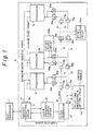
- the selectors 11a 1 , 11a 2 , ⁇ 11a n are provided on the clock signal supply path 15 at the locations corresponding to the locations of the selectors 9a 1 , 9a 2 , ⁇ 9a n on the return path 16.
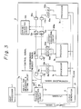
- FIG. 3 is a block diagram showing a construction of the second embodiment of the present invention.
- reference numeral 2' denotes a parallel data processing apparatus
- 5' denotes a request reception circuit
- 6b 1 , 6b 2 , ⁇ 6b n each denote a programmable delay circuit
- 7b denotes a delay time measuring & setting circuit
- 9b 1 , 9b 2 , ⁇ 9b n each denote a selector
- 10b 1 , 10b 2 , ⁇ 10b n each denote a programmable delay circuit
- 11b 1 , 11b 2 , ⁇ 11b n each denote a selector
- 12b 2 denotes an offset adjusting circuit
- 13b and 13b' each denote a waveform shaping circuit
- 14b denotes an offset adjusting circuit
- 15 denotes a clock signal supply path
- 16 denotes a clock signal return path
- 17 denotes an asynchronous request signal path
- 18 de
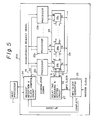
- Fig. 4 is an embodiment of the above-mentioned third aspect of the present invention.
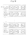
- the provision for adjusting propagation delay times to the plurality of processors 3 1 , 3 2 , ⁇ 3 n is made for both the construction for supplying the asynchronous request signal and the construction for supplying the clock signal, where the respective provisions are the same as those shown in Figs. 1 and 3.
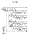
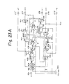
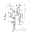
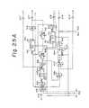
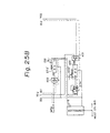
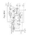
- reference numerals 250, 252, 257, and 259 each denote a buffer amplifier
- 251, 254, 255, and 258 each denote a selector
- 253 and 256 each denote a programmable delay circuit.
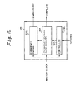
- reference numerals A to G respectively correspond to the denotations of the terminals of Fig. 5.
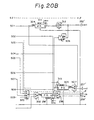
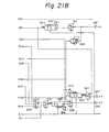
- the selector 302 is provided for selecting one of the routes to be used when initially adjusting the delay times in the programmable delay circuits 253 1 to 253 4 , and a route to be used when measuring propagation delay times for the respective processors 22 1 to 22 4 .
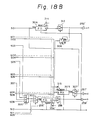
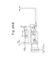
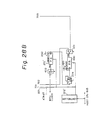
- the selector 401 is provided for selecting one of a route for use when initially adjusting the delay times in the programmable delay circuits 272', and a route for use when measuring the propagation delay times.
- the selector 402 is provided for the symmetry with the provision of the selector 401.
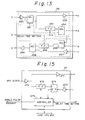
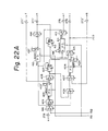
- the programmable delay circuit 403 is provided for adjusting a delay time in a path from the input port for the MPU clock signal or the input port e to the output port f.
- the programmable delay circuit 404 is provided for initially adjusting a delay time in the programmable delay circuit 403.
- the D-type flip-flop circuit 405 is provided for use when determining initial delay times in the programmable delay circuits 403 and 404.
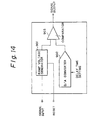
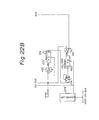
- the programmable delay circuit 410 is provided for adjusting a delay time in a path from the input port for the MPU clock signal or the input port e to the output port h, and shaping a waveform of a signal passing therethrough.
- the programmable delay circuit 411 is provided for adjusting a delay time in a path from the input port i to the output port j, and shaping a waveform of a signal passing therethrough.
- the D-type flip-flop circuit 412 is provided for determining initial delay times in the programmable delay circuits 410 and 411.
- the selector 413 is provided for selecting one of a route to be used when initially adjusting the delay times in the programmable delay circuits 410 and 411, and a route to be used when measuring the propagation delay times.
Landscapes
- Engineering & Computer Science (AREA)
- Theoretical Computer Science (AREA)
- Physics & Mathematics (AREA)
- General Engineering & Computer Science (AREA)
- General Physics & Mathematics (AREA)
- Multi Processors (AREA)
- Test And Diagnosis Of Digital Computers (AREA)
Claims (14)
- Gerät zum Zuführen eines durch Datenverarbeitungseinheiten (31, 32, ..., 3n) gleichzeitig zu empfangenden Signals, umfassend:gekennzeichnet durcheine Mehrzahl erster Signalpfade (15, 33a1, 33a2, ..., 33an), jeder zum Zuführen des Signals von einer gemeinsamen Position zu einer der Datenverarbeitungseinheiten,eine Mehrzahl zweiter Signalpfade (16, 34a1, 34a2, ..., 34an), jeder zum Rückleiten des Signals von einer der Datenverarbeitungseinheiten zur gemeinsamen Position, wo jeder der Mehrzahl zweiter Signalpfade mit einem entsprechenden der ersten Signalpfade ein Paar bildet,ein Offset-Einstellmittel (12a) zum anfänglichen Ausgleichen von Signalausbreitungsverzögerungen in den ersten und zweiten Signalpfaden jedes Paares,ein Verzögerungsmeßmittel (7a) zum Messen von Verzögerungen, während sich das Signal von der gemeinsamen Position zu den Datenverarbeitungseinheiten ausbreitet und dann durch jedes Paar der ersten und zweiten Signalpfade zur gemeinsamen Position zurückgeleitet wird, undein Verzögerungseinstellmittel (7a) zum Einstellen der durch das Meßmittel gemessenen Verzögerungen, um Verzögerungen in allen Paaren der ersten und zweiten Signalpfade auszugleichen.
- Gerät nach Anspruch 1, worin jeder der ersten und zweiten Signalpfade in der Mehrzahl von Paaren von Signalpfaden Variable-Verzögerung-Mittel (6a1, 6a2, ..., 6an, 10a1, 10a2, ..., 10an) zum Verzögern einer Ausbreitung des Signals durch die ersten und zweiten Signalpfade aufweist.
- Gerät nach Anspruch 2, worin das Verzögerungseinstellmittel die Verzögerungen, die durch die Variable-Verzögerung-Mittel (6a1, 6a2, ..., 6an, 10a1, 10a2, ..., 10an) in den ersten und zweiten Signalpfaden von jedem der Mehrzahl von Paaren von Signalpfaden verursacht werden, auf der Grundlage einer durch das Verzögerungsmeßmittel (7a) durchgeführten Messung einstellt.
- Gerät nach einem der Ansprüche 2 oder 3, worin das Offset-Einstellmittel (12a) Verzögerungen zu Anfang einstellt, die durch die Variable-Verzögerung-Mittel in den ersten und zweiten Signalpfaden von jedem der Mehrzahl von Paaren von Signalpfaden verursacht werden, bevor das Verzögerungsmeßmittel die Verzögerung mißt.
- Gerät nach einem der Ansprüche 1 bis 4, worin der erste Signalpfad (15, 33a1, 33a2, ..., 33an) von jedem der Mehrzahl von Paaren von Signalpfaden einen gemeinsamen Zuführungsseite-Pfad (15) gemeinsam nutzt, der gemeinsame Zuführungsseite-Pfad mindestens ein Verzweigungsmittel (11a1, 11a2, ..., 11an) aufweist, jedes zum Verzweigen des Signals von dem gemeinsamen Zuführungsseite-Pfad zu dem Zuführungsseite-Verzweigungspfad, welcher Zuführungsseite-Verzweigungspfad das Signal von jedem Verzweigungsmittel zum entsprechenden Prozessor ausbreitet, und der zweite Signalpfad von jedem der Mehrzahl von Paaren von Signalpfaden (16, 34a1, 34a2, ..., 34an) einen gemeinsamen Rückleitungsseite-Pfad (16) gemeinsam nutzt, der gemeinsame Rückleitungsseite-Pfad mindestens einen Rückleitungsseite-Verzweigungspfad zum Ausbreiten des Signals vom entsprechenden Prozessor zum gemeinsamen Rückleitungsseite-Pfad und mindestens ein Verbindungsmittel aufweist, jedes zum Verbinden eines des mindestens einen Rückleitungsseite-Verzweigungspfades mit dem gemeinsamen Rückleitungsseite-Pfad.
- Gerät nach einem der Ansprüche 2 bis 5, worin das Variable-Verzögerung-Mittel auf jedem von dem Zuführungsseite-Verzweigungspfad und dem Rückleitungsseite-Verzweigungspfad vorgesehen ist.
- Gerät nach einem der Ansprüche 2 bis 5, worin das Variable-Verzögerung-Mittel auf jedem von dem gemeinsamem Zuführungsseite-Pfad und dem gemeinsamen Rückleitungsseite-Pfad vorgesehen ist.
- Gerät nach einem der Ansprüche 5 bis 7, worin die Mehrzahl von Prozessoren (31, 32, ..., 3n) in einer vorbestimmten Reihenfolge angeordnet ist, wobei der gemeinsame Rückleitungsseite-Pfad (16) mit der Mehrzahl von Prozessoren durch mindestens eines des mindestens einen Verbindungsmittels (9a1, 9a2, ..., 9an) und einem des mindestens einen Rückleitungsseite-Verzweigungspfades verbunden ist, und jedes Verbindungsmittel (9a1, 9a2, ..., 9an) einen Selektor zum Empfangen eines ersten Signals aufweist, das sich von einem des mindestens einen Rückleitungsseite-Verzweigungspfades ausbreitet, und eines zweiten Signals, das sich von dem gemeinsamen Rückleitungsseite-Pfad (16) auf der stromaufwärtigen Seite des Selektors ausbreitet, Auswählen eines der ersten und zweiten Signale, was ein ausgewähltes Signal ergibt, und Abgeben des ausgewählten Signals auf dem gemeinsamen Rückleitungsseite-Pfad (16) auf der stromabwärtigen Seite des Selektors.
- Gerät nach einem der Ansprüche 1 bis 8, ferner umfassend Wellenform-Formermittel (13a, 13a', 13b, 13b') in jedem der ersten und zweiten Signalpfade von jedem der Mehrzahl von Paaren zum Formen des Signals, wenn das Signal durch die Wellenform-Formermittel übertragen wird.
- Gerät zum Paralleldatenverarbeiten nach einem der Ansprüche 1 bis 9, umfassend:eine Mehrzahl von Prozessoren (31, 32, ..., 3n) zum Parallelverarbeiten von Daten, welche Mehrzahl von Prozessoren synchron mit einem gemeinsamen Taktsignal verarbeitet, und Starten einer Operation auf ein Empfangen eines gemeinsamen asynchronen Anforderungssignals hin; undTakterzeugungsmittel (4) zum Erzeugen eines gemeinsamen Taktsignals, das der Mehrzahl von Prozessoren zugeführt werden soll;welches Paralleldatenverarbeitungsgerät ferner das Gerät, wie in einem der Ansprüche 1 und 5 beschrieben, zum Zuführen eines vorbestimmten des gemeinsamen Taktsignals und des gemeinsamen asynchronen Anforderungssignals als das in Anspruch 1 beschriebene Signal zur Mehrzahl von Prozessoren als die in Anspruch 1 beschriebenen Datenverarbeitungseinheiten aufweist.
- Gerät nach Anspruch 10, worin eine Mehrzahl von Signalpfaden (17) durch eine Verdrahtung mit gleichen Längen zum Zuführen des anderen des gemeinsamen Taktsignals und des gemeinsamen asynchronen Anforderungssignals zur Mehrzahl von Prozessoren realisiert ist.
- Gerät nach einem der Ansprüche 10 oder 11, ferner umfassend:eine außerhalb des Paralleldatenverarbeitungsgeräts gelegene Vorrichtung zum Zuführen des gemeinsamen asynchronen Anforderungssignals;ein Steuermittel (24) für einen Empfang des asynchronen Anforderungssignals zum Empfangen des gemeinsamen asynchronen Anforderungssignals, das von der außerhalb des Paralleldatenverarbeitungsgeräts gelegenen Vorrichtung zugeführt wird; undein Taktfrequenzsteuermittel (23) zum vorübergehenden Verringern einer Frequenz des gemeinsamen Taktsignals auf eine vorbestimmte Frequenz, wenn das Steuermittel für einen Empfang eines asynchronen Anforderungssignals das gemeinsame asynchrone Anforderungssignal empfängt, das von der außerhalb des Paralleldatenverarbeitungsgeräts gelegenen Vorrichtung zugeführt wird; undwelches Steuermittel (24) für einen Empfang eines asynchronen Anforderungssignals das gemeinsame asynchrone Anforderungssignal jedem der Mehrzahl von Prozessoren zuführt, wenn die Frequenz des gemeinsamen Taktsignals auf die vorbestimmte Frequenz verringert ist.
- Verfahren zum Zuführen eines durch Prozessoren gleichzeitig zu empfangenden Signals, umfassend die Schritte:gekennzeichnet durch(a) Zuführen des Signals von einer gemeinsamen Position durch eine Mehrzahl von Signalzuführungspfaden zu den Prozessoren,(b) Rückleiten des Signals von den Prozessoren durch eine Mehrzahl von Signalrückleitungspfaden zu der gemeinsamen Position, wo jeder der Mehrzahl von Signalrückleitungspfaden mit einem entsprechenden der Signalzuführungspfade ein Paar bildet,(c) anfängliches Ausgleichen von Signalausbreitungsverzögerungen in dem Signalzuführungspfad und dem Signalrückleitungspfad jedes Paares,(d) Messen von Verzögerungen, während sich das Signal von der gemeinsamen Position zu den Prozessoren ausbreitet und dann durch jedes Paar der Signalzuführungs- und Signalrückleitungspfade zur gemeinsamen Position zurückgeleitet wird, und(e) Einstellen der im Schritt (d) gemessenen Verzögerungen, um Verzögerungen in allen Paaren der Signalzuführungs- und Signalrückleitungspfade auszugleichen.
- Paralleldatenverarbeitungssystem, umfassend:eine Mehrzahl von Prozessoren (31, 32 ..., 3n) zum Parallelverarbeiten von Daten, welche Mehrzahl von Prozessoren synchron mit einem gemeinsamen Taktsignal verarbeitet, und Starten einer Operation auf ein Empfangen eines gemeinsamen asynchronen Anforderungssignals hin; undein Takterzeugungsmittel (4) zum Erzeugen eines gemeinsamen Taktsignals, das der Mehrzahl von Prozessoren zugeführt werden soll;welches Paralleldatenverarbeitungssystem ferner aufweistein erstes Gerät, mit der Konstruktion wie in einem der Ansprüche 1 bis 9 beschrieben, zum Zuführen des gemeinsamen Taktsignals als das in Anspruch 1 beschriebene Signal zur Mehrzahl von Prozessoren als die in Anspruch 1 beschriebenen Datenverarbeitungseinheiten; undein zweites Gerät, mit der Konstruktion wie in einem der Ansprüche 1 bis 9 beschrieben, zum Zuführen des gemeinsamen asynchronen Anforderungssignals als das in Anspruch 1 beschriebene Signal zur Mehrzahl von Prozessoren als die in Anspruch 1 beschriebenen Datenverarbeitungseinheiten.
Applications Claiming Priority (3)
| Application Number | Priority Date | Filing Date | Title |
|---|---|---|---|
| JP171069/90 | 1990-06-28 | ||
| JP2171069A JP2507677B2 (ja) | 1990-06-28 | 1990-06-28 | 分散型デ―タ処理装置 |
| JP17106990 | 1990-06-28 |
Publications (3)
| Publication Number | Publication Date |
|---|---|
| EP0464632A2 EP0464632A2 (de) | 1992-01-08 |
| EP0464632A3 EP0464632A3 (en) | 1993-08-25 |
| EP0464632B1 true EP0464632B1 (de) | 1999-12-08 |
Family
ID=15916461
Family Applications (1)
| Application Number | Title | Priority Date | Filing Date |
|---|---|---|---|
| EP91110561A Expired - Lifetime EP0464632B1 (de) | 1990-06-28 | 1991-06-26 | Paralleles Datenverarbeitungssystem und -verfahren mit Signalverschiebungskompensation |
Country Status (6)
| Country | Link |
|---|---|
| US (1) | US5220660A (de) |
| EP (1) | EP0464632B1 (de) |
| JP (1) | JP2507677B2 (de) |
| AU (1) | AU636768B2 (de) |
| DE (1) | DE69131822T2 (de) |
| FI (1) | FI913114A7 (de) |
Families Citing this family (27)
| Publication number | Priority date | Publication date | Assignee | Title |
|---|---|---|---|---|
| US5577214A (en) * | 1992-05-18 | 1996-11-19 | Opti, Inc. | Programmable hold delay |
| US5615358A (en) * | 1992-05-28 | 1997-03-25 | Texas Instruments Incorporated | Time skewing arrangement for operating memory in synchronism with a data processor |
| JPH0793386A (ja) * | 1993-09-28 | 1995-04-07 | Fujitsu Ltd | Lsi実装設計システム |
| US5467465A (en) * | 1993-11-17 | 1995-11-14 | Umax Data System Inc. | Two clock method for synchronizing a plurality of identical processors connected in parallel |
| JPH07248847A (ja) * | 1994-03-11 | 1995-09-26 | Fujitsu Ltd | クロック信号調整方法および装置 |
| US5768620A (en) * | 1996-04-09 | 1998-06-16 | International Business Machines Corporation | Variable timeout method in a missing-interrupt-handler for I/O requests issued by the same operating system |
| US6115769A (en) * | 1996-06-28 | 2000-09-05 | Lsi Logic Corporation | Method and apparatus for providing precise circuit delays |
| US6557066B1 (en) | 1999-05-25 | 2003-04-29 | Lsi Logic Corporation | Method and apparatus for data dependent, dual level output driver |
| US6294937B1 (en) | 1999-05-25 | 2001-09-25 | Lsi Logic Corporation | Method and apparatus for self correcting parallel I/O circuitry |
| DE10006236C2 (de) * | 2000-02-11 | 2001-12-20 | Infineon Technologies Ag | Anordnung zum Generieren von Signalimpulsen mit definierten Pulslängen in einem Baustein mit BIST-Funktion |
| JP3628265B2 (ja) * | 2001-02-21 | 2005-03-09 | 株式会社半導体理工学研究センター | マルチプロセッサシステム装置 |
| KR100414943B1 (ko) * | 2001-12-28 | 2004-01-16 | 엘지전자 주식회사 | 콤팩트 피씨아이에 기반한 다중 처리 시스템에서의 클럭분배 장치 및 방법 |
| US7043649B2 (en) * | 2002-11-20 | 2006-05-09 | Portalplayer, Inc. | System clock power management for chips with multiple processing modules |
| US7698490B2 (en) * | 2005-12-21 | 2010-04-13 | Nvidia Corporation | Passive USB power configuration switching |
| US7414550B1 (en) | 2006-06-30 | 2008-08-19 | Nvidia Corporation | Methods and systems for sample rate conversion and sample clock synchronization |
| US9209792B1 (en) | 2007-08-15 | 2015-12-08 | Nvidia Corporation | Clock selection system and method |
| US9088176B2 (en) * | 2007-12-17 | 2015-07-21 | Nvidia Corporation | Power management efficiency using DC-DC and linear regulators in conjunction |
| US8327173B2 (en) * | 2007-12-17 | 2012-12-04 | Nvidia Corporation | Integrated circuit device core power down independent of peripheral device operation |
| US9411390B2 (en) | 2008-02-11 | 2016-08-09 | Nvidia Corporation | Integrated circuit device having power domains and partitions based on use case power optimization |
| US9423846B2 (en) | 2008-04-10 | 2016-08-23 | Nvidia Corporation | Powered ring to maintain IO state independent of the core of an integrated circuit device |
| US8762759B2 (en) * | 2008-04-10 | 2014-06-24 | Nvidia Corporation | Responding to interrupts while in a reduced power state |
| JP5604799B2 (ja) * | 2009-03-06 | 2014-10-15 | 日本電気株式会社 | フォールトトレラントコンピュータ |
| JP5800752B2 (ja) * | 2012-04-25 | 2015-10-28 | 三菱電機株式会社 | 信号源同期回路 |
| US9395799B2 (en) | 2012-08-09 | 2016-07-19 | Nvidia Corporation | Power management techniques for USB interfaces |
| US9471395B2 (en) | 2012-08-23 | 2016-10-18 | Nvidia Corporation | Processor cluster migration techniques |
| US20140062561A1 (en) | 2012-09-05 | 2014-03-06 | Nvidia Corporation | Schmitt receiver systems and methods for high-voltage input signals |
| EP2775655B1 (de) * | 2013-03-08 | 2020-10-28 | Pro Design Electronic GmbH | Verfahren zum Verteilen eines Taktsignals, Taktverteilungssystem und elektronisches System, umfassend ein Taktverteilungssystem |
Family Cites Families (7)
| Publication number | Priority date | Publication date | Assignee | Title |
|---|---|---|---|---|
| US4063308A (en) * | 1975-06-27 | 1977-12-13 | International Business Machines Corporation | Automatic clock tuning and measuring system for LSI computers |
| US4769558A (en) * | 1986-07-09 | 1988-09-06 | Eta Systems, Inc. | Integrated circuit clock bus layout delay system |
| JPS63238714A (ja) * | 1986-11-26 | 1988-10-04 | Hitachi Ltd | クロック供給システム |
| US4805196A (en) * | 1987-04-29 | 1989-02-14 | Gte Laboratories Incorporated | Line delay compensation for digital transmission systems utilizing low power line drivers |
| US5086500A (en) * | 1987-08-07 | 1992-02-04 | Tektronix, Inc. | Synchronized system by adjusting independently clock signals arriving at a plurality of integrated circuits |
| US5041966A (en) * | 1987-10-06 | 1991-08-20 | Nec Corporation | Partially distributed method for clock synchronization |
| US4868522A (en) * | 1988-12-13 | 1989-09-19 | Gazelle Microcircuits, Inc. | Clock signal distribution device |
-
1990
- 1990-06-28 JP JP2171069A patent/JP2507677B2/ja not_active Expired - Fee Related
-
1991
- 1991-06-25 AU AU79273/91A patent/AU636768B2/en not_active Ceased
- 1991-06-26 EP EP91110561A patent/EP0464632B1/de not_active Expired - Lifetime
- 1991-06-26 DE DE69131822T patent/DE69131822T2/de not_active Expired - Fee Related
- 1991-06-26 FI FI913114A patent/FI913114A7/fi unknown
- 1991-06-27 US US07/722,198 patent/US5220660A/en not_active Expired - Lifetime
Also Published As
| Publication number | Publication date |
|---|---|
| JP2507677B2 (ja) | 1996-06-12 |
| DE69131822D1 (de) | 2000-01-13 |
| EP0464632A3 (en) | 1993-08-25 |
| FI913114A7 (fi) | 1991-12-29 |
| DE69131822T2 (de) | 2000-04-06 |
| AU636768B2 (en) | 1993-05-06 |
| EP0464632A2 (de) | 1992-01-08 |
| US5220660A (en) | 1993-06-15 |
| JPH0460742A (ja) | 1992-02-26 |
| FI913114A0 (fi) | 1991-06-26 |
| AU7927391A (en) | 1992-03-26 |
Similar Documents
| Publication | Publication Date | Title |
|---|---|---|
| EP0464632A2 (de) | Paralleles Datenverarbeitungssystem mit einem Verschiebungskompensationssignal | |
| EP0871931B1 (de) | System zur phasenanpassung für eine synchrone logische schaltung | |
| US5414381A (en) | Method of adjusting for clock skew | |
| US5184027A (en) | Clock signal supply system | |
| WO2020135332A1 (zh) | 一种时间同步方法及电子设备 | |
| EP3788732B1 (de) | System und verfahren zur vervollständigung eines kaskadierten taktringbusses | |
| JPH0218658A (ja) | データ処理装置 | |
| US7280550B1 (en) | Bandwidth optimization of ring topology through propagation delay compensation | |
| CN112711296A (zh) | 一种校准系统 | |
| US5235566A (en) | Clock skew measurement technique | |
| US6509775B2 (en) | Synchronous delay circuit and semiconductor integrated circuit apparatus | |
| CN101512358A (zh) | 产生时间参考的设备及方法 | |
| JP3409739B2 (ja) | 自動スキュー調整装置 | |
| CN101373639A (zh) | 存储器时序测量电路与其测试方法 | |
| EP0282735B1 (de) | Taktsignal-Versorgungssystem | |
| TW201409944A (zh) | 多相位時脈除頻器 | |
| Tu et al. | A hybrid communication topology for modular multilevel converter | |
| US8901938B2 (en) | Delay line scheme with no exit tree | |
| JP3527161B2 (ja) | 半導体集積回路装置及びクロックスキューの検証方法 | |
| JPS59144927A (ja) | タイミング調整回路 | |
| JPH0566851A (ja) | 複数の回路ブロツクへのタイミング信号付与方法 | |
| JP4553428B2 (ja) | プログラム可能なずれ及び周波数を有するフェーズロックループ(pll)・クロック発生器 | |
| CN112087224B (zh) | 时间同步分配输入接口电路及其延时补偿的方法 | |
| CN120629894A (zh) | 一种芯片测试系统、方法和电子设备 | |
| JPH05275988A (ja) | 信号遅延方法、信号遅延装置及び信号遅延装置用回路 |
Legal Events
| Date | Code | Title | Description |
|---|---|---|---|
| PUAI | Public reference made under article 153(3) epc to a published international application that has entered the european phase |
Free format text: ORIGINAL CODE: 0009012 |
|
| AK | Designated contracting states |
Kind code of ref document: A2 Designated state(s): DE FR GB |
|
| PUAL | Search report despatched |
Free format text: ORIGINAL CODE: 0009013 |
|
| AK | Designated contracting states |
Kind code of ref document: A3 Designated state(s): DE FR GB |
|
| 17P | Request for examination filed |
Effective date: 19940218 |
|
| 17Q | First examination report despatched |
Effective date: 19970813 |
|
| GRAG | Despatch of communication of intention to grant |
Free format text: ORIGINAL CODE: EPIDOS AGRA |
|
| GRAG | Despatch of communication of intention to grant |
Free format text: ORIGINAL CODE: EPIDOS AGRA |
|
| GRAH | Despatch of communication of intention to grant a patent |
Free format text: ORIGINAL CODE: EPIDOS IGRA |
|
| GRAH | Despatch of communication of intention to grant a patent |
Free format text: ORIGINAL CODE: EPIDOS IGRA |
|
| GRAA | (expected) grant |
Free format text: ORIGINAL CODE: 0009210 |
|
| AK | Designated contracting states |
Kind code of ref document: B1 Designated state(s): DE FR GB |
|
| PG25 | Lapsed in a contracting state [announced via postgrant information from national office to epo] |
Ref country code: FR Free format text: LAPSE BECAUSE OF FAILURE TO SUBMIT A TRANSLATION OF THE DESCRIPTION OR TO PAY THE FEE WITHIN THE PRESCRIBED TIME-LIMIT Effective date: 19991208 |
|
| REF | Corresponds to: |
Ref document number: 69131822 Country of ref document: DE Date of ref document: 20000113 |
|
| EN | Fr: translation not filed | ||
| PLBE | No opposition filed within time limit |
Free format text: ORIGINAL CODE: 0009261 |
|
| STAA | Information on the status of an ep patent application or granted ep patent |
Free format text: STATUS: NO OPPOSITION FILED WITHIN TIME LIMIT |
|
| 26N | No opposition filed | ||
| REG | Reference to a national code |
Ref country code: GB Ref legal event code: IF02 |
|
| PGFP | Annual fee paid to national office [announced via postgrant information from national office to epo] |
Ref country code: GB Payment date: 20060621 Year of fee payment: 16 |
|
| PGFP | Annual fee paid to national office [announced via postgrant information from national office to epo] |
Ref country code: DE Payment date: 20060622 Year of fee payment: 16 |
|
| GBPC | Gb: european patent ceased through non-payment of renewal fee |
Effective date: 20070626 |
|
| PG25 | Lapsed in a contracting state [announced via postgrant information from national office to epo] |
Ref country code: DE Free format text: LAPSE BECAUSE OF NON-PAYMENT OF DUE FEES Effective date: 20080101 |
|
| PG25 | Lapsed in a contracting state [announced via postgrant information from national office to epo] |
Ref country code: GB Free format text: LAPSE BECAUSE OF NON-PAYMENT OF DUE FEES Effective date: 20070626 |