EP0466394A2 - Connecteur d'assemblage - Google Patents
Connecteur d'assemblage Download PDFInfo
- Publication number
- EP0466394A2 EP0466394A2 EP91306055A EP91306055A EP0466394A2 EP 0466394 A2 EP0466394 A2 EP 0466394A2 EP 91306055 A EP91306055 A EP 91306055A EP 91306055 A EP91306055 A EP 91306055A EP 0466394 A2 EP0466394 A2 EP 0466394A2
- Authority
- EP
- European Patent Office
- Prior art keywords
- disks
- bus
- parallel
- crossbar switch
- processing
- Prior art date
- Legal status (The legal status is an assumption and is not a legal conclusion. Google has not performed a legal analysis and makes no representation as to the accuracy of the status listed.)
- Withdrawn
Links
Images



Classifications
-
- G—PHYSICS
- G06—COMPUTING OR CALCULATING; COUNTING
- G06F—ELECTRIC DIGITAL DATA PROCESSING
- G06F13/00—Interconnection of, or transfer of information or other signals between, memories, input/output devices or central processing units
- G06F13/38—Information transfer, e.g. on bus
- G06F13/40—Bus structure
- G06F13/4063—Device-to-bus coupling
- G06F13/409—Mechanical coupling
-
- G—PHYSICS
- G06—COMPUTING OR CALCULATING; COUNTING
- G06F—ELECTRIC DIGITAL DATA PROCESSING
- G06F15/00—Digital computers in general; Data processing equipment in general
- G06F15/16—Combinations of two or more digital computers each having at least an arithmetic unit, a program unit and a register, e.g. for a simultaneous processing of several programs
-
- H—ELECTRICITY
- H05—ELECTRIC TECHNIQUES NOT OTHERWISE PROVIDED FOR
- H05K—PRINTED CIRCUITS; CASINGS OR CONSTRUCTIONAL DETAILS OF ELECTRIC APPARATUS; MANUFACTURE OF ASSEMBLAGES OF ELECTRICAL COMPONENTS
- H05K7/00—Constructional details common to different types of electric apparatus
- H05K7/14—Mounting supporting structure in casing or on frame or rack
- H05K7/1438—Back panels or connecting means therefor; Terminals; Coding means to avoid wrong insertion
- H05K7/1439—Back panel mother boards
- H05K7/1442—Back panel mother boards with a radial structure
Definitions
- the present invention relates to a connector assembly for a parallel-processing device which permits a plurality of processing units such as processors or memories to perform their processings simultaneously, substantially reducing the time involved for different processings.
- processing units such as processors or memories
- parallel-processing devices are appropriate, for instance, for processing color image data at high speed.
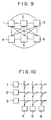
- One kind of parallel processing device is a complete connection type in which a plurality of processing elements 1 through 6 such as processors or memories are connected together by a plurality of buses, as shown in Fig. 9.
- the other kind of processing device uses a crossbar switch to interconnect a plurality of processing elements 1 through 6, as shown in Fig. 10.
- the number of crossing contacts in the crossbar switch will increase with the number of the processing elements to be connected, and accordingly the device will become bulky. Because of relatively long transmission distance, a disadvantage still exists, however in that the device will likely be subjected to interference by exterior noise signals, and that the device will produce noise signals.
- a connector assembly for connecting a plurality of processing elements in a parallel-processing device comprises a plurality of bus disks arranged along a common axis, each disk having an integrated circuit crossbar switch at its centre and a plurality of signal conductor lines of substantially equal length radially extending thereon from the crossbar switch to the circumference of respective bus disks for connection to processing elements wherein the switch is controllable to open and close an interior contact at each crossing of the signal conductor lines in the crossbar switch according to a predetermined sequence.
- the present invention enables a parallel-processing device to be provided which permits data-processing at an increased speed and which is insensitive to noise signals.
- the present invention also enables a parallel-processing device to be provided whose size can be substantially reduced.
- the signal conductor lines radiating from the center crossbar switch on each disk constitute parallel buses, and can be allotted to data lines, address lines, control lines and the like.
- a control means performs the opening-and-closing operation of all contacts in the crossbar switch according to a predetermined sequence.
- processing units such as processors, memories and the like can be selectively electrically connected at one time through the agency of the crossbar switch and associated conductor lines, thereby permitting simultaneous transmission of data between selected processing units and simultaneous processing of data by such selected processing units.
- the crossbar switch is an integrated circuit, and therefore, it is very small, and the signal conductor lines radiating from the center crossbar switch are of equal length. Consequently, all processing units can be interconnected by conductor lines of equal length. Therefore, the transmission distance between selected processing units are substantially equalized. This makes it possible to perform accurate, high-speed transmission control, and hence high-speed data processing.
- bus disks in the form of a pile permits interconnection of numerous processing units via conductor lines of relatively short length radiating from the center crossbar switch, thus rendering them less sensitive to noise signals because of a shortened transmission distance between selected processing units.
- the use of the pile of bus disks permits reduction of the device size.
- a bus disk 7 which has a plurality of conductor lines 13 printed on its circular board 8 and radiating from a center crossbar switch 9.
- the crossbar switch 9 is built in the form of an integrated circuit. As seen from Fig. 2, the crossbar switch has one contact 11 at each crossing of vertical and horizontal signal conductor lines 10. Each signal conductor line 10 in the crossbar switch 9 is terminated at terminal 12 for exterior connection.
- a plurality of conductor lines 13 of equal length are connected to the terminals 12 of the crossbar switch 9. These conductor lines 13 radiate from the crossbar switch 9 on the printed board 8, ending with terminals 14 for exterior connection.
- the crossbar switch 9 has a plurality of control terminals 15 for controlling the opening-and-closing of contacts at crossings (although shown as a single tip in the drawing for the sake of simplicity), and the plurality of control conductor lines 16 are printed on the board and are connected to the control terminals 15 (although shown as a single line in the drawingfor the sake of simplicity).
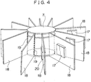
- a plurality of bus disks 7 each bearing a crossbar switch and a plurality of conductor lines radiating therefrom, are vertically arranged along one common axis at regular intervals.
- the communication conductor lines 13 and crossbar switch control conductor lines 16 are arranged at regular angular intervals.
- the communication conductor lines 13 are to be used as parallel buses, and to be allotted and used as data lines, address lines, control lines and the like.
- a plurality of upright printed boards 18 each bearing a processing unit 17 are arranged radially around a pile of bus disks.
- Each upright printed board 18 has a plwality of terminals 19 for exterior connection on its inner vertical edge. These terminals are electrically connected to corresponding terminals 14 on the circumference of each bus disk 7 via connectors (not shown).
- a selected printed board 18 is equipped with a crossbar switch controller 20, which is connected to the crossbar switch control line 16 of each bus disk, thereby controlling the opening-and-closing of each crossing contact 11 in the crossbar switch 9.
- the processing units 17 which are fixed on the printed boards 18 may be central processing units, memories, and input/output processors for controlling the input/output devices of keyboards or display devices.
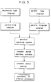
- a program according to which a given task such as color imaging processing is performed is prepared in sequential type language such as FORTRAN or in parallel type language, and stored in memories.
- a parallelizing compiler will find out which parts of the program can be parallel-performed, and then it will rearrange such parts in parallel tasks. With the program expressed in the parallel type language, a parallel language compiler will selectively pick up parallel parts so that parallel machine codes may be prepared.
- the operating system of the parallel machine will carry out dynamic allotment of processors, and the switching controlling schedule of each crossbar switch will be prepared on the basis of the allotment of processors. In this way parallel-processing will be handled.
- the crossbar switch controller 20 performs the switching of all crossing contacts 11 in each crossbar switch 9 according to the schedule, thereby permitting all processing units 17 to process data simultaneously.
- Disks are described as having a crossbar switch and radiating conductor lines on one side. As a matter of course, disks may have a crossbar switch and conductor lines on opposite sides. Otherwise, they may be a multi-layered or lamination disk having a crossbar switch and conductor lines printed on each layer.
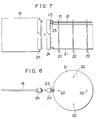
- FIG. 6 one example of a three-layered bus disk is described below.
- the bus disk 21 is composed of upper, intermediate and lower layers each having communication conductor lines 13A, 13B or 13C.
- the communication conductor lines of the upper, intermediate and lower layers are arranged offset relative to each of the other layers. These conductor lines 13A, 13B and 13C are terminated by terminals 14A, 14B and 14C, respectively.
- such lamination bus disks 21 are arranged vertically and are integrated by four upright rods 22 in the same fashion as in Fig. 4.
- the terminals 14A, 14B and 14C of each bus disk 21 are connected to a female receptacle 24, which has pins 23 arranged in three lines.
- Each printed board 18 has a male plug 25 on its inner vertical edge. All printed boards can be connected to the pile of disks 21 by mating the male plugs 25 of the printed boards 18 with the female receptacles 24 of the bus disks 21 (See Figs. 7 and 8).
- lamination disks makes it possible to substantially increase the density and compactness of elements in a parallel-processing device, and accordingly reduce the size of the device.
- a parallel-processing device In the case where a parallel-processing device according to the present invention is used in processing color-image data and outputting the processed data to a display device, red, green and blue data retrieved from different memories are further processed, and then the processed data are further transferred to selected I/O CPUs by controlling the crossbar switch of the parallel-processing device, thus omitting transmission of data between memories.
- a parallel-processing device In the case where a parallel-processing device according to the present invention is used in color printing, selected CPUs of the parallel processing device are allotted to yellow, cyan, magenta, and black to perform required processings simultaneously.
- processing large amounts of data it is possible to store divisions of data in different sections of a selected memory, thereby permitting distribution of the CPUs'processing domain. In this case data transmission can be omitted, and accordingly quick processing results are achieved.
- a parallel-processing device In the case where a parallel-processing device according to the present invention is used in the production of motion pictures such as animated cartoons, one CPU can be allotted to each frame to perform necessary processing, thereby permitting real time processing.
- a parallel-processing device uses a pile of bus disks each having an integrated circuit crossbar switch at its center and a plurality 'of conductor lines radiating from the center crossbar switch, thus providing communication lines of equal length to make a required electrical connection between selected processing units. This eliminates the necessity of adjusting different transmission times in communication between selected processing units, and accordingly the time involved for processing is shortened.
- a pile of numerous disks permit interconnection of numerous processing units therearound through the shortest possible conductor lines, thus making the processing units insensitive to interference by noise signals.
Landscapes
- Engineering & Computer Science (AREA)
- Theoretical Computer Science (AREA)
- Computer Hardware Design (AREA)
- General Engineering & Computer Science (AREA)
- Physics & Mathematics (AREA)
- General Physics & Mathematics (AREA)
- Microelectronics & Electronic Packaging (AREA)
- Software Systems (AREA)
- Multi Processors (AREA)
Applications Claiming Priority (2)
| Application Number | Priority Date | Filing Date | Title |
|---|---|---|---|
| JP180995/90 | 1990-07-09 | ||
| JP2180995A JPH0743699B2 (ja) | 1990-07-09 | 1990-07-09 | 並列処理装置 |
Publications (2)
| Publication Number | Publication Date |
|---|---|
| EP0466394A2 true EP0466394A2 (fr) | 1992-01-15 |
| EP0466394A3 EP0466394A3 (en) | 1993-05-12 |
Family
ID=16092896
Family Applications (1)
| Application Number | Title | Priority Date | Filing Date |
|---|---|---|---|
| EP19910306055 Withdrawn EP0466394A3 (en) | 1990-07-09 | 1991-07-03 | Connector assembly |
Country Status (7)
| Country | Link |
|---|---|
| EP (1) | EP0466394A3 (fr) |
| JP (1) | JPH0743699B2 (fr) |
| KR (1) | KR920003188A (fr) |
| AU (1) | AU7938691A (fr) |
| CA (1) | CA2045431A1 (fr) |
| IL (1) | IL98591A0 (fr) |
| NZ (1) | NZ238799A (fr) |
Cited By (5)
| Publication number | Priority date | Publication date | Assignee | Title |
|---|---|---|---|---|
| EP0509765A1 (fr) * | 1991-04-19 | 1992-10-21 | Graphico Co. Ltd. | Assemblage radial de bus |
| EP0486231A3 (en) * | 1990-11-16 | 1993-05-12 | Graphico Co. Ltd. | Parallel processing system |
| WO1993015464A1 (fr) * | 1992-01-30 | 1993-08-05 | Ralph Harold Kelly | Fond de panier d'ordinateur a commutateurs de lignes |
| EP0594200A3 (fr) * | 1992-10-22 | 1995-01-25 | Digital Equipment Corp | Câblage d'un fond de panier pour un boîtier central d'un réseau de commutation de paquets de données. |
| US20240314930A1 (en) * | 2023-03-14 | 2024-09-19 | Samsung Electronics Co., Ltd. | Computing system with connecting boards |
Families Citing this family (1)
| Publication number | Priority date | Publication date | Assignee | Title |
|---|---|---|---|---|
| CA2323964A1 (fr) * | 1998-03-12 | 1999-09-16 | Hironori Akamatsu | Selecteur de bus et systeme de circuit integre |
Family Cites Families (3)
| Publication number | Priority date | Publication date | Assignee | Title |
|---|---|---|---|---|
| US4456965A (en) * | 1980-10-14 | 1984-06-26 | Texas Instruments Incorporated | Data processing system having multiple buses |
| CH664662A5 (en) * | 1986-02-26 | 1988-03-15 | Valtronic S A | Interconnecting device for electronic cards in star formation - has upright around insulating central core contg. conductive connectors for mating with edge connectors |
| JP2591677B2 (ja) * | 1989-04-21 | 1997-03-19 | 株式会社 グラフィコ | 放射型・パラレル・システムバス |
-
1990
- 1990-07-09 JP JP2180995A patent/JPH0743699B2/ja not_active Expired - Lifetime
-
1991
- 1991-06-24 IL IL98591A patent/IL98591A0/xx unknown
- 1991-06-25 CA CA002045431A patent/CA2045431A1/fr not_active Abandoned
- 1991-06-27 AU AU79386/91A patent/AU7938691A/en not_active Abandoned
- 1991-06-28 NZ NZ238799A patent/NZ238799A/en unknown
- 1991-07-01 KR KR1019910011086A patent/KR920003188A/ko not_active Ceased
- 1991-07-03 EP EP19910306055 patent/EP0466394A3/en not_active Withdrawn
Cited By (5)
| Publication number | Priority date | Publication date | Assignee | Title |
|---|---|---|---|---|
| EP0486231A3 (en) * | 1990-11-16 | 1993-05-12 | Graphico Co. Ltd. | Parallel processing system |
| EP0509765A1 (fr) * | 1991-04-19 | 1992-10-21 | Graphico Co. Ltd. | Assemblage radial de bus |
| WO1993015464A1 (fr) * | 1992-01-30 | 1993-08-05 | Ralph Harold Kelly | Fond de panier d'ordinateur a commutateurs de lignes |
| EP0594200A3 (fr) * | 1992-10-22 | 1995-01-25 | Digital Equipment Corp | Câblage d'un fond de panier pour un boîtier central d'un réseau de commutation de paquets de données. |
| US20240314930A1 (en) * | 2023-03-14 | 2024-09-19 | Samsung Electronics Co., Ltd. | Computing system with connecting boards |
Also Published As
| Publication number | Publication date |
|---|---|
| KR920003188A (ko) | 1992-02-29 |
| EP0466394A3 (en) | 1993-05-12 |
| JPH0468462A (ja) | 1992-03-04 |
| IL98591A0 (en) | 1992-07-15 |
| CA2045431A1 (fr) | 1992-01-10 |
| JPH0743699B2 (ja) | 1995-05-15 |
| NZ238799A (en) | 1994-06-27 |
| AU7938691A (en) | 1992-01-09 |
Similar Documents
| Publication | Publication Date | Title |
|---|---|---|
| US5301089A (en) | Parallel processing system | |
| US3333225A (en) | Connector | |
| JPH0584924B2 (fr) | ||
| US5341509A (en) | Parallel processing system including a stack of bus-printed disks and a plurality of radially exending processing unit boards | |
| US3796848A (en) | Pin connector switch | |
| JPH11317489A (ja) | メモリモジュ―ル板 | |
| US6349037B1 (en) | Backplane for common building block | |
| US20260101441A1 (en) | Board and server | |
| EP0466394A2 (fr) | Connecteur d'assemblage | |
| US6244881B1 (en) | Connector, data processing apparatus, and network apparatus | |
| US6578103B1 (en) | Compact PCI backplane and method of data transfer across the compact PCI backplane | |
| EP0520706A1 (fr) | Commutateur à joints de croisement et système de traitement de données en parallèle l'utilisant | |
| AU673386B2 (en) | LAN interface | |
| JPS6227409B2 (fr) | ||
| JPS59161097A (ja) | フラツトケ−ブル型星型接続装置 | |
| JP2592759B2 (ja) | 分配器 | |
| GB2153567A (en) | Arrangements for enabling the connection of one or more additional devices to a computer | |
| JPS6130100A (ja) | 電気的構成ユニツト | |
| JPH0212754Y2 (fr) | ||
| JPH04181410A (ja) | 並列処理装置 | |
| JPH04191956A (ja) | 並列処理装置 | |
| JPS60140687A (ja) | プリント回路の接続装置 | |
| JPH052445U (ja) | インピーダンス整合器 | |
| JPH0619692B2 (ja) | ラジアル・バス | |
| JPS58144205A (ja) | 電子装置 |
Legal Events
| Date | Code | Title | Description |
|---|---|---|---|
| PUAI | Public reference made under article 153(3) epc to a published international application that has entered the european phase |
Free format text: ORIGINAL CODE: 0009012 |
|
| AK | Designated contracting states |
Kind code of ref document: A2 Designated state(s): AT BE CH DE DK ES FR GB GR IT LI LU NL SE |
|
| 17P | Request for examination filed |
Effective date: 19920626 |
|
| PUAL | Search report despatched |
Free format text: ORIGINAL CODE: 0009013 |
|
| AK | Designated contracting states |
Kind code of ref document: A3 Designated state(s): AT BE CH DE DK ES FR GB GR IT LI LU NL SE |
|
| STAA | Information on the status of an ep patent application or granted ep patent |
Free format text: STATUS: THE APPLICATION HAS BEEN WITHDRAWN |
|
| 18W | Application withdrawn |
Withdrawal date: 19930719 |
|
| R18W | Application withdrawn (corrected) |
Effective date: 19930719 |