EP0466500A2 - Verarbeitungsgerät für ein orthogonales Multiplexsignal - Google Patents
Verarbeitungsgerät für ein orthogonales Multiplexsignal Download PDFInfo
- Publication number
- EP0466500A2 EP0466500A2 EP91306335A EP91306335A EP0466500A2 EP 0466500 A2 EP0466500 A2 EP 0466500A2 EP 91306335 A EP91306335 A EP 91306335A EP 91306335 A EP91306335 A EP 91306335A EP 0466500 A2 EP0466500 A2 EP 0466500A2
- Authority
- EP
- European Patent Office
- Prior art keywords
- signal
- reference signal
- period
- specific
- sub
- Prior art date
- Legal status (The legal status is an assumption and is not a legal conclusion. Google has not performed a legal analysis and makes no representation as to the accuracy of the status listed.)
- Withdrawn
Links
Images


Classifications
-
- H—ELECTRICITY
- H04—ELECTRIC COMMUNICATION TECHNIQUE
- H04N—PICTORIAL COMMUNICATION, e.g. TELEVISION
- H04N5/00—Details of television systems
- H04N5/14—Picture signal circuitry for video frequency region
- H04N5/21—Circuitry for suppressing or minimising disturbance, e.g. moiré or halo
- H04N5/211—Ghost signal cancellation
-
- H—ELECTRICITY
- H04—ELECTRIC COMMUNICATION TECHNIQUE
- H04N—PICTORIAL COMMUNICATION, e.g. TELEVISION
- H04N7/00—Television systems
- H04N7/01—Conversion of standards, e.g. involving analogue television standards or digital television standards processed at pixel level
-
- H—ELECTRICITY
- H04—ELECTRIC COMMUNICATION TECHNIQUE
- H04L—TRANSMISSION OF DIGITAL INFORMATION, e.g. TELEGRAPHIC COMMUNICATION
- H04L25/00—Baseband systems
- H04L25/02—Details ; arrangements for supplying electrical power along data transmission lines
- H04L25/0202—Channel estimation
- H04L25/0224—Channel estimation using sounding signals
- H04L25/0226—Channel estimation using sounding signals sounding signals per se
-
- H—ELECTRICITY
- H04—ELECTRIC COMMUNICATION TECHNIQUE
- H04L—TRANSMISSION OF DIGITAL INFORMATION, e.g. TELEGRAPHIC COMMUNICATION
- H04L25/00—Baseband systems
- H04L25/02—Details ; arrangements for supplying electrical power along data transmission lines
- H04L25/03—Shaping networks in transmitter or receiver, e.g. adaptive shaping networks
- H04L25/03006—Arrangements for removing intersymbol interference
- H04L25/03012—Arrangements for removing intersymbol interference operating in the time domain
- H04L25/03114—Arrangements for removing intersymbol interference operating in the time domain non-adaptive, i.e. not adjustable, manually adjustable, or adjustable only during the reception of special signals
-
- H—ELECTRICITY
- H04—ELECTRIC COMMUNICATION TECHNIQUE
- H04N—PICTORIAL COMMUNICATION, e.g. TELEVISION
- H04N21/00—Selective content distribution, e.g. interactive television or video on demand [VOD]
- H04N21/40—Client devices specifically adapted for the reception of or interaction with content, e.g. set-top-box [STB]; Operations thereof
- H04N21/41—Structure of client; Structure of client peripherals
- H04N21/426—Internal components of the client ; Characteristics thereof
-
- H—ELECTRICITY
- H04—ELECTRIC COMMUNICATION TECHNIQUE
- H04N—PICTORIAL COMMUNICATION, e.g. TELEVISION
- H04N7/00—Television systems
- H04N7/08—Systems for the simultaneous or sequential transmission of more than one television signal, e.g. additional information signals, the signals occupying wholly or partially the same frequency band, e.g. by time division
- H04N7/087—Systems for the simultaneous or sequential transmission of more than one television signal, e.g. additional information signals, the signals occupying wholly or partially the same frequency band, e.g. by time division with signal insertion during the vertical blanking interval only
Definitions
- the present invention relates to an orthogonal multiplex signal processing apparatus which is suitable for a television signal transmission and receiving system.
- a frequency spectra has double sidebands symmetrical in the range of ⁇ 1.25 MHz around a video carrier frequency. If, therefore, television signals are limited to this frequency band, an orthogonal biaxial modulation is available for tramsmitting any sub signal in addition to conventional video signals.
- an AM-modulated wave is represented by the following expression. ⁇ 1 + p(t) ⁇ cos ⁇ ct
- the desired wave expressed by the equation (1) only includes the component "cos ⁇ ct", but it is seen that the component " ⁇ n ⁇ 1 + p(t - ⁇ n) ⁇ sin ⁇ n” is generated as a quadrature component "sin ⁇ ct" in the ghost wave expressed by the equation (2) in addition to the component "cos ⁇ ct".
- Synchronous Demodulated In-phase Component p(t) + ⁇ ⁇ n cos ⁇ n p(t - ⁇ n)
- Equation (6) indicates that the crosstalk of quadrature component is generated by ghosts.
- This value is generally observed as a delay group on actual equipment.
- the ghost image trouble that has become an issue is long distance ghost image showing a picture doubly or trebly.
- a two-dimensional filter is effective for two-dimensional transmission using orthogonal modulation.
- the one dimensional reference signal to be used for standard video signals has been decided after various discussions and the multiplex transmission of a reference waveform on a time-sharing basis in the vertical blanking period commenced in regular broadcasting in 1989.
- the present invention has been made to obtain a system which processes two-dimensional reference signals effectively without affecting unidimensional reference signals for video signals.
- the orthogonal multiplex When the orthogonal multiplex is considered as a new service to be added to the conventional broadcasting service, the compatibility with the conventional broadcasting service is required.
- the orthogonal multiplex component is regarded as noise and becomes a disturbance component for conventional receivers.
- the present invention therfore seeks to provide an orthogonal multiplex signal processing apparatus which is compatible with the current broadcasting system and enables it to realize the effective waveform equalization of orthogonal signal.
- An orthogonal multiplex signal processing apparatus has a first inserting circuit for inserting a reference signal into a first specific period within a vertical blanking period of the main signal, a second inserting circuit for inserting a second reference signal into every other frame of the main signal in a second specific period of within a vertical blanking period of the main signal, a first interrupting circuit for interrupting the transmission of the first reference signal to inspect for ghost images of the sub signal in the first specific period and its immediately preceding scanning period and a second interrupting circuit for interrupting the transmission of the second reference signal to inspect for ghosts of the sub signal in the second specific period of frames in which the second reference signal is not inserted.
- the orthogonal multiplex of signals at VSB modulation which is used in the current NTSC system broadcasting is considered.
- xp(t) is modulated in-phase with a carrier using the VSB modulation in the DSB region and yp(t) is orthogonally modulated and multiplexed.
- xp(t) is AM-modulated as usual and yp(t) is AM-modulated in a suppressed-carrier manner.
- the receiving signal with the ghost wave superimposed is expressed by the following equation: where, ⁇ n and ⁇ m are coefficients of ghost image amplitude, respectively.
- detected outputs have a linear relation in connection with xp and yp.
- the television signal can be considered by disregarding DC components. Therefore, if 1 + ⁇ an cos ⁇ n in the equation (18) and ⁇ an sin ⁇ n in the equation (12) are omitted, the equation (18) and (19) will become as follows:
- equalization outputs are obtained as the same "x" and "y” as those at the transmitter.
- GCR ghost cancel reference
- the present invention has been made based on the principle described above.
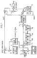
- FIGURE 1 shows the construction of the transmitter in one embodiment of the present invention.
- the current NTSC signal is input to the terminal 1 and the GCR signal for in-phase signal is inserted in the adder 2.
- the GCRx signal is output from the in-phase GCR generator 4 and supplied to the adder 2 through the switch 3. Switch 3 is controlled by the timing generator 22.
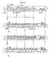
- the switch 3 is turned ON in 18H and 281H of the vertical blanking period as shown in FIGURE 2. "H” indicates the horizontal period.
- the main signal with the GCRx signal superimposed in the adder 2 in this way during the specific scanning period is multiplied with the in-phase carrier "cos ⁇ ct" in the multiplier 5.
- the inphase modulated main signal is obtained from the multiplier 5.
- This in-phase modulated signal is input to the adder 6.
- the timing generator 22 turns ON the switch 13 in 1H - 9H (see FIGURE 2) and introduces the quadrature signal's GCRy signal into the adder 12.
- the GCRy signal is generated in the quadrature GCR generator 14.
- the GCRy signal is added to sub signal in the adder 12.
- Output from the adder 12 is input to the adder 15 in Mode 2. Output from this adder 15 is fedback to the adder 15 through the delay units 16a and 16b.
- This filter output is input to the subtractor 17 and the delay unit 18. Output from the delay unit 18 is input to the subtractor 17.
- a differential value obtained from the subtractor 17 is supplied to the spectrum shaping filter 19.
- This spectrum shaping filter 19 has the frequency characteristic of "cos ⁇ fT".
- the adder 15, delay unit 16a, 16b and 18, subtractor 17 and spectrum shaping filter 19 are provided for making the spectra of sub signals transmitted uniform, preencoding them to make waveform equalization at the receiver easy, and at the same time, when transmitting sub signals, limiting the frequency band to prevent the modulated signal from interfering with television signals.
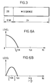
- FIGURE 3 shows an example of GCRy signal.
- the clock line signal (CRI data) is transmitted for 0.5H as a sampling clock reference at the receiver and thereafter, random data (for instance, M sequence) is transmitted for 2H.
- Uniformly distributed spectra are desirable for random data from the viewpoint of equalization characteristics at the receiver. Therefore, when the random data period is extended, the spectrum will become more dense and advantageous, but about 2H is sufficient for practical use.
- FIGURE 4 shows an example of CRI data processing in progress.
- FIGURE 4A is digital input
- FIGURE 4B is preencoded output
- FIGURE 4C is output from the adder 17
- FIGURE 4D is output from the spectrum shaping filter.
- FIGURE 5 shown an example of random data processing progress.
- FIGURE 5A is digital random input
- FIGURE 5B is pre-encoded output
- FIGURE 5C is output from the adder 17
- FIGURE 5D is output from the spectrum shaping filter 19.
- the GCRy signal is processed so that spectra are uniformly distributed to make waveform equalization easy.
- FIGURE 6A shows the characteristic of the spectrum shaping filter 19.
- Output from this spectrum shaping filter 19 is input to the multiplier 20.
- the in-phase carrier of cos ⁇ ct is phase shifted by the ⁇ /2 phase shifter 21 to form the orthogonal carrier and supplied to the multiplier 20. Therefore, the output from the multiplier 20 becomes an orthogonal modulated signal.
- This orthogonal modulated signal is input to the adder 6 and then after being combined with the previous in-phase modulated signal, band limited by the band-pass filter (BPF) 23 and output to the transmission system.
- BPF band-pass filter
- "1/4 fck” has the relation of line inversion and has the effect of reducing visual interference on a TV set currently in use. Further, as "1/2 fck" is 1 MHz, orthogonal multiplex in the VSB modulated DSB region is possible.
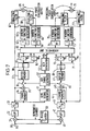
- FIGURE 7 shows an example at the receiver of this system.
- Picture intermediate frequency (PIF) of the received channel is supplied to the multipliers 31 and 41 via the terminal 30.
- PIF Picture intermediate frequency
- the multiplier 31 multiplication of PIF and reproduced carrier "sin ⁇ ct" (the phase shifted reproduced carrier “cos ⁇ ct" by the ⁇ /2 phase shifter 50) is carried out and the orthogonal synchronous detection is performed.
- Outputs from the multipliers 31 and 41 are input to and digitized in the analog/digital (A/D) converters 33 and 43, respectively via the low-pass filters (LPF) 32 and 42.
- A/D analog/digital
- LPF low-pass filters
- the output signal (NTSC signal) from the A/D converter 33 is input to the waveform equalizing filter 67 and the ghost image is cancelled here.
- the output signal (sub signal) from the A/D converter 43 is input to the waveform equalizing filter 77 and the ghost image is cancelled here.
- the output from the A/D converter 33 is input to the sync. signal generator 51.
- the sync. signal generator 51 the horizontal and vertical synchronizing signals and CRI signal are reproduced. These synchronizing signals are input to the GCR timing generator 52.
- the GCR timing generator 52 outputs pulses at the timing synchronizing with the GCR signals GCRx and GCRy and controls the switches 36 and 46.
- the switch 36 is turned ON at the timings of 18H and 281H.
- the switch 46 is turned ON at the timing of 1H - 9H (or 263H - 272H).
- the output from the A/D converter 33 is input to the frame memory 34 and also, to the subtractor 35 to which the output from the frame memory 34 is supplied. Therefore, the inter-frame differential signal is obtained from the subtractor 35. Further, the output from the analog/ digital converter 43 is also input to the frame memory 44 and the subtractor 45 to which the output from the frame memory 44 is supplied. Therefore, the inter-frame differential signal is obtained from the subtractor 45.
- the inter-frame differential signal taken out by the switch 36 is temporarily stored in the buffer memory 37 and converted to the frequency region by the high-speed Fourier converter (referred to as FFT hereafter) 38. Further, the inter-frame differential signal taken out by the switch 46 is temporarily stored in the buffer memory 47 and converted to the frequency region by the FFT 48.
- FFT high-speed Fourier converter
- the output from the Fourier converter 38 is input to the dividers 61 and 62 and the output from the Fourier converter 48 is input to the dividers 71 and 72.
- the division by Rx is performed and in the dividers 62 and 72, the division by Rx and Ry is performed.
- Rx and Ry are generated by the GCR generator 53 synchronized with the timing signal from the GCR timing generator 52 .
- These Rx and Ry are the reference signal waveforms shown in the equations (36), (37), (38) and (39) presented previously. Further, the outputs from the constrained Fourier converters 38 and 48 are the detection outputs "u” and "v”.
- the input to the equalizing filter 67 is the inphase demodulated signal and the input to the equalizing filter 68 is the orthogonal demodulated signal. So, the component (ghost) to which the sub signal is crosstalked is also removed. The outputs from the equalizing filters 67 and 68 are combined in the adder 69 and output as the equalization output of in-phase demodulated signal.
- the input to the equalizing filter 77 is the orthogonal demodulated signal and the input to the equalizing filter 78 is the in-phase demodulated signal. So, the component (ghost) to which the main signal is crosstalked is also removed. The outputs from the equalizing filters 77 and 78 are combined in the adder 79 and output as the equalization output of orthogonal demodulated signal.
- FIGURE 8 Shown in FIGURE 8 is another embodiment at the receiver. The same symbols are assigned to the same parts as shown in FIGURE 7.
- C1, C2, C3 and C4 are to be approximately constructed by the non-cyclic type limited length (FIR) filters.
- FIR non-cyclic type limited length
- the output from the A/D converter 33 is supplied to the frame memory 34 and the subtractor to which the output from the frame memory 34 is supplied. Further, the output from the A/D converter 43 is supplied to the frame memory 44 and to the subtractor 45 to which the output from the frame memory 44 is supplied.
- the switches 81 and 91 select the outputs from the subtractors 35 and 45 only when corresponding GCR signals arrive, and normally select the outputs from the A/D converters 33 and 43 and introduce them into the corresponding waveform equalizing filters.
- the output from the switch 81 is supplied to the waveform equalizing filters 84 and 95, and the correlators 83 and 96.
- the output from the switch 91 is supplied to the waveform equalizing filter 85 and the correlator 86.
- the outputs from the waveform equalizing filters 84 and 85 are combined in the adder 87 and led to the output terminal 201 as the in-phase demodulated output and at the same time, input to the subtractor 102. Further, the outputs from the waveform equalizing filters 95 and 94 are also combined in the adder 97 and led to the output terminal 202 as the orthogonal demodulated output and at the same time, input to the subtractor 112.
- the sync. signal generator 51 reproduces the synchronizing signal and CRI signal from the output from the A/D converter 33 and supplies these reproduced outputs to the CRR timing generator 52.
- the GCR generators 101 and 111 Based on this output signal from the GCR timing generator 52, the GCR generators 101 and 111 generate the in-phase and orthogonal reference waveform signals r(p) and r(q), respectively. Differing from the previously shown embodiment, these signals become time domain signals.
- the ghost information that is, error signals (the results of operations by the equations (35) and (36)) are obtained and these error signals are input to the correlators 83 and 86, and 93 and 96.
- the operations of the equations (44) - (47) are performed using the error signals and input signals to correct the tap coefficients of the corresponding equalizing filters.
- the inter-frame difference signal taken by the frame memory 34 and the subtractor 35 is input to the correlators 83 and 96, while the inter-frame difference signal taken by the frame memory 44 and the substractor 45 is input to the correlator 86.
- sub signals can be orthogonally modulated and multiplexed without impeding the ghost cancelling operation in the current television broadcasting.
- multiplex signals by orthogonal modulation cannot be put to practical use in the television broadcasting unless a secondary equalizing filter for orthogonal multiplex is realized.
- transmission of reference signals suited for orthogonal multiplexing which is compatible with the current broadcasting system and accurate reproduction of reference signals at a receiver are possible and therefore, the two dimensional equalizing filter can be accurately controlled at the receiver and a practical use of sub signals which are orthogonally multiplexed and transmitted becomes possible.
- the present invention can provide an extremely preferable orthogonal multiplex signal processing apparatus.
Landscapes
- Engineering & Computer Science (AREA)
- Signal Processing (AREA)
- Multimedia (AREA)
- Power Engineering (AREA)
- Computer Networks & Wireless Communication (AREA)
- Picture Signal Circuits (AREA)
- Television Systems (AREA)
Applications Claiming Priority (2)
| Application Number | Priority Date | Filing Date | Title |
|---|---|---|---|
| JP2182601A JPH0472874A (ja) | 1990-07-12 | 1990-07-12 | 直交多重信号処理装置 |
| JP182601/90 | 1990-07-12 |
Publications (2)
| Publication Number | Publication Date |
|---|---|
| EP0466500A2 true EP0466500A2 (de) | 1992-01-15 |
| EP0466500A3 EP0466500A3 (en) | 1992-06-03 |
Family
ID=16121142
Family Applications (1)
| Application Number | Title | Priority Date | Filing Date |
|---|---|---|---|
| EP19910306335 Withdrawn EP0466500A3 (en) | 1990-07-12 | 1991-07-12 | Orthogonal multiplex signal processing apparatus |
Country Status (4)
| Country | Link |
|---|---|
| EP (1) | EP0466500A3 (de) |
| JP (1) | JPH0472874A (de) |
| KR (1) | KR940011601B1 (de) |
| CA (1) | CA2046946A1 (de) |
Cited By (4)
| Publication number | Priority date | Publication date | Assignee | Title |
|---|---|---|---|---|
| EP0577351A3 (en) * | 1992-06-30 | 1994-09-28 | Matsushita Electric Industrial Co Ltd | Television signal processing apparatus |
| US5371548A (en) * | 1993-07-09 | 1994-12-06 | Cable Television Laboratories, Inc. | System for transmission of digital data using orthogonal frequency division multiplexing |
| EP0654944A1 (de) * | 1993-11-18 | 1995-05-24 | Lg Electronics Inc. | Kanalentzerrer für Fernsehempfänger |
| EP0663765A1 (de) * | 1994-01-18 | 1995-07-19 | Daewoo Electronics Co., Ltd | Kanalschnittstelleneinrichtung zum Verbessern der Konvergenzgeschwindigkeit eines adaptiven Entzerrers nach dem Verfahren des kleinsten quadratischen Fehlers |
Families Citing this family (1)
| Publication number | Priority date | Publication date | Assignee | Title |
|---|---|---|---|---|
| KR20020042888A (ko) * | 2000-12-01 | 2002-06-08 | 구광시 | 광학활성을 지닌 (s)-2-(6'-메톡시-2'-나프틸)프로피온산및 그 유도체의 신규한 제조방법 |
Family Cites Families (1)
| Publication number | Priority date | Publication date | Assignee | Title |
|---|---|---|---|---|
| US4882614A (en) * | 1986-07-14 | 1989-11-21 | Matsushita Electric Industrial Co., Ltd. | Multiplex signal processing apparatus |
-
1990
- 1990-07-12 JP JP2182601A patent/JPH0472874A/ja active Pending
-
1991
- 1991-07-12 EP EP19910306335 patent/EP0466500A3/en not_active Withdrawn
- 1991-07-12 KR KR1019910011855A patent/KR940011601B1/ko not_active Expired - Lifetime
- 1991-07-12 CA CA002046946A patent/CA2046946A1/en not_active Abandoned
Cited By (5)
| Publication number | Priority date | Publication date | Assignee | Title |
|---|---|---|---|---|
| EP0577351A3 (en) * | 1992-06-30 | 1994-09-28 | Matsushita Electric Industrial Co Ltd | Television signal processing apparatus |
| US5371548A (en) * | 1993-07-09 | 1994-12-06 | Cable Television Laboratories, Inc. | System for transmission of digital data using orthogonal frequency division multiplexing |
| EP0654944A1 (de) * | 1993-11-18 | 1995-05-24 | Lg Electronics Inc. | Kanalentzerrer für Fernsehempfänger |
| US5654765A (en) * | 1993-11-18 | 1997-08-05 | Goldstar Co., Ltd. | Channel equalizer for digital television receiver having an initial coefficient storage unit |
| EP0663765A1 (de) * | 1994-01-18 | 1995-07-19 | Daewoo Electronics Co., Ltd | Kanalschnittstelleneinrichtung zum Verbessern der Konvergenzgeschwindigkeit eines adaptiven Entzerrers nach dem Verfahren des kleinsten quadratischen Fehlers |
Also Published As
| Publication number | Publication date |
|---|---|
| EP0466500A3 (en) | 1992-06-03 |
| KR920003778A (ko) | 1992-02-29 |
| JPH0472874A (ja) | 1992-03-06 |
| CA2046946A1 (en) | 1992-01-13 |
| KR940011601B1 (ko) | 1994-12-22 |
Similar Documents
| Publication | Publication Date | Title |
|---|---|---|
| KR910002634B1 (ko) | 다중신호 처리장치 | |
| US5621471A (en) | System and method for inserting and recovering an add-on data signal for transmission with a video signal | |
| US5276507A (en) | Multiplex TV signal processing apparatus | |
| EP0466500A2 (de) | Verarbeitungsgerät für ein orthogonales Multiplexsignal | |
| JPS6019376A (ja) | 3つのテレビジヨン信号時間・周波数多重化技術 | |
| KR0123189B1 (ko) | 파형등화기 | |
| KR940008122B1 (ko) | Tv신호 다중전송장치 | |
| JP2615478B2 (ja) | テレビジョン信号送信方法とテレビジョン信号受信方法 | |
| JPH07105920B2 (ja) | 妨害波除去受信装置 | |
| JP2003518839A (ja) | 既存の通信伝送システムのための拡大された情報容量に関する受信器の改良 | |
| JP2529948B2 (ja) | 画像信号伝送システム | |
| JPS63240194A (ja) | 多重伝送方式およびその信号発生装置 | |
| JP2715407B2 (ja) | テレビジヨン信号処理方法 | |
| JPH0621841A (ja) | 伝送信号再生装置 | |
| JP2834124B2 (ja) | 多重伝送方法およびその信号発生装置 | |
| JPH082103B2 (ja) | 高精細テレビジョン | |
| JPH0514868A (ja) | クロストーク除去装置及びクロストーク除去方法 | |
| JPH0460393B2 (de) | ||
| JPH07226726A (ja) | Ofdm伝送方法並びにofdm送信装置及びofdm受信装置 | |
| JPH0691652B2 (ja) | テレビ信号伝送方法 | |
| JPH05137087A (ja) | テレビジヨン信号復調装置 | |
| JPH06315100A (ja) | 波形等化器 | |
| JPH02156786A (ja) | 多重伝送方法およびそのための送受信装置 | |
| JPH0418867A (ja) | 多重伝送方法及びその送信側に用いる信号発生装置と受信側に用いる信号再生装置 | |
| JPH06284314A (ja) | 波形等化器 |
Legal Events
| Date | Code | Title | Description |
|---|---|---|---|
| PUAI | Public reference made under article 153(3) epc to a published international application that has entered the european phase |
Free format text: ORIGINAL CODE: 0009012 |
|
| 17P | Request for examination filed |
Effective date: 19910802 |
|
| AK | Designated contracting states |
Kind code of ref document: A2 Designated state(s): DE FR NL |
|
| PUAL | Search report despatched |
Free format text: ORIGINAL CODE: 0009013 |
|
| AK | Designated contracting states |
Kind code of ref document: A3 Designated state(s): DE FR NL |
|
| STAA | Information on the status of an ep patent application or granted ep patent |
Free format text: STATUS: THE APPLICATION HAS BEEN WITHDRAWN |
|
| 18W | Application withdrawn |
Withdrawal date: 19920612 |
|
| R18W | Application withdrawn (corrected) |
Effective date: 19920611 |
|
| R18W | Application withdrawn (corrected) |
Effective date: 19920611 |