EP0471846A1 - Systeme de controleurs de sequence - Google Patents
Systeme de controleurs de sequence Download PDFInfo
- Publication number
- EP0471846A1 EP0471846A1 EP90907501A EP90907501A EP0471846A1 EP 0471846 A1 EP0471846 A1 EP 0471846A1 EP 90907501 A EP90907501 A EP 90907501A EP 90907501 A EP90907501 A EP 90907501A EP 0471846 A1 EP0471846 A1 EP 0471846A1
- Authority
- EP
- European Patent Office
- Prior art keywords
- controller system
- module
- cpu
- modules
- cpu module
- Prior art date
- Legal status (The legal status is an assumption and is not a legal conclusion. Google has not performed a legal analysis and makes no representation as to the accuracy of the status listed.)
- Withdrawn
Links
Images


Classifications
-
- G—PHYSICS
- G05—CONTROLLING; REGULATING
- G05B—CONTROL OR REGULATING SYSTEMS IN GENERAL; FUNCTIONAL ELEMENTS OF SUCH SYSTEMS; MONITORING OR TESTING ARRANGEMENTS FOR SUCH SYSTEMS OR ELEMENTS
- G05B19/00—Program-control systems
- G05B19/02—Program-control systems electric
- G05B19/04—Program control other than numerical control, i.e. in sequence controllers or logic controllers
- G05B19/042—Program control other than numerical control, i.e. in sequence controllers or logic controllers using digital processors
- G05B19/0421—Multiprocessor system
Definitions
- the present invention relates to a sequence controller system and, more particularly, to a small-sized, low-priced, modular type sequence controller system comprising a plurality of CPU's and a plurality of I/O units.
- a large-scale system under control is divided conventionally into blocks each assigned to a sequence controller, control of each block being confined to its assigned sequence controller.
- To control any two blocks in coordination under this prior art control scheme requires exchanging data between the two controllers corresponding to these blocks.
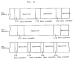
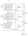
- Fig. 12 illustrates an example in which the above prior art scheme is implemented. This example involves the process of assembling products in three blocks.
- coordinated control is provided between assembling apparatus A and B and subsequently between assembling apparatus B and C for consecutive product assembly.
- the assembling apparatus A, B and C are controlled by a first, a second and a third controller system, respectively.
- the controller systems each comprise an input module 101 and an output module 102.
- the first and second controller systems exchange data through their input and output modules 101 and 102.
- the second and third controller systems do the same through their input and output modules 101 and 102.
- each controller comprising a small CPU and an I/O unit.
- the same data is supplied to all sequence controllers over the transfer lines.
- each sequence controller processes the data and outputs the result through its I/O unit according to a preset program. What is missing from this disclosure is any consideration for the data transfer between sequence controllers.
- a sequence controller system comprising a first controller system and a second controller system, the first controller system further comprising a first CPU module and at least one first I/O module connected to the first CPU module, the second controller system further comprising a second CPU module and and at least one second I/O module connected to the second CPU module.
- One of the modules has a buffer that stores the data to be transmitted between the first and the second controller systems. The buffer is controlled so as to start and stop data transmission between the first and the second controller systems.
- the CPU module of the second system contains a buffer which prevents the data from the upstream system from being transmitted direct to the I/O module of the second system.
- Each I/O module has a conducting means that forwards data to the next module.
- Each CPU module is capable of disconnecting signal transmission lines so that the system in which it is incorporated is made distinct from the other systems.
- each I/O module may expand the scope of the system in which it is contained.
- One advantage of the present invention is that a plurality of CPU modules and the I/O modules connected thereto may be located where desired, each group of the CPU and I/O modules working as an independent controller.
- Another advantage of the invention is that the data exchange, carried out between CPU modules simultaneously with I/O data transfer, involves less delays. This eliminates the need for a module arrangement dedicated to the data exchange function. To sum up, the sequence controller system according to the invention is produced in small size and at low cost, provides control at high speeds and prevents delays during coordinated control operations.
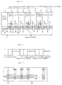
- the first embodiment is constituted by a mother board 30 at the bottom of an open-ended, box-shaped base 7, the mother board 30 being equipped thereon with slots 32 as connectors accommodating a power supply module 1, a CPU module 2 and an I/O module 3, the slots being interconnected by signal lines 8.
- the wiring between the slots 32 on the mother board 30 comprises data transmission lines 8a and address lines 8b which connect output terminals 32b of one slot 32 to input terminals 32a of the adjoining slot 32, as well as the lines such as power supply lines 34 and slot identification lines 36 which are continuously connected to and installed across the slots.
- the output terminals 32b are electrically shielded from the input terminals 32a.
- the power supply module 1 is connected to the leftmost slot 32 on the mother board 30.
- the other modules are powered by the power supply module 1 via the power supply lines 34.
- the power supply module 1 is mechanically connected to the slot 32 and electrically connected to the power supply terminals 32c which in turn are connected to the power lines 34.
- the output terminals 32b are electrically shielded from the input terminals 32a.
- the power supply terminals 32c are also connected to such lines as the slot identification lines 36 that are continuously connected to and installed across the slots.
- Fig. 3 Adjacent to the power supply module 1 is a first controller system, which in turn is adjoined by a second controller system, which is adjoined by a third, and so on.
- Fig. 3 shows an example in which three controller systems are interconnected.
- the CPU modules used in the systems may be of the same type.
- the CPU module of the second system is illustratively identified by reference numeral 4 and that of the third system by 6.
- On the mother board 30 in the base 7 are the signal lines 8 and the power supply lines 34.
- the signal lines 8 are needed to transfer data between the CPU modules 2, 4 and 6 and between the I/O modules 3.
- the power supply lines 34 are provided to convey power from the power supply module 11 to the other modules.
- the signal lines 8 comprise data transmission lines 8a and address lines 8b.
- the signal lines passing from the CPU modules 2, 4 and 6 through the I/O modules 3 are relayed by each I/O module.
- the signal lines 8 on the mother board 30 are wired independently between two adjacent slots 32.
- Each CPU module is connected to its I/O module via a connector 33.
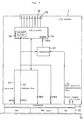
- Fig. 4 depicts how the CPU modules 2, 4 and 6 are arranged in the first embodiment.
- the CPU modules 2, 4 and 6 each contain a CPU 19; a user memory 20 and a data memory 21 connected to the CPU 19; a data bus 40a and an address bus 42a for forwarding signals from the input terminals 32a of the slot 32 to a dual port RAM 23 which serves as an insulating means; a data bus 40b for allowing data to be exchanged between the dual port RAM 23 and the CPU 19; an address bus 42b for sending an address signal from the CPU 19 to the dual port RAM 23; a data bus 40b for exchanging data with the output terminals 32b; a data bus 40c which is connected to the data bus 40b and which exchanges signals with the data bus 40d via a buffer 22a; an address bus 42c for supplying a buffer 22b with the address signal from the CPU 19; an address bus 42d for supplying the address signal to the output terminals 32b via the buffer 22b; an I/O transfer interface 22 having the buffers 22a
- the data buses 40a and 40b and the address buses 42a and 42d each comprise eight lines to configure an eight-bit bus structure.
- the dual port RAM 23, acting as the insulating means, provides signal insulation between the data buses 40a and 40d as well as between the address buses 42a and 42d.
- the bidirectional buffer 22a containing registers and other parts are interposed between the data buses 40d and 40c.
- the buffer 22a permits bidirectional signal transmission between the CPU 19 and the I/O module 3.
- the unidirectional buffer 22b containing registers and other parts is interposed between the address buses 42d and 42c.
- the buffer 22b permits unidirectional signal transmission from the CPU 19 to the I/O module 3.
- the CPU modules 2, 4 and 6 are powered by the power supply module 1 via the power supply terminals 32c and the connector 33 of the slots 32, the power supply lines from the connector 33 to the modules are omitted in Fig. 4.
- the CPU modules detect their slot locations using position information tapped from the slot identification lines 36.
- Fig. 5 shows the construction of one I/O module 3 used in the first embodiment.
- the I/O module 3 has a data bus 50 and an address bus 52 connected to the connector 33, the data bus 50 serving as the conducting means to connect the input terminals 32a to the output terminals 32b within the same slot 32.
- the data bus 50 is provided so as to permit bidirectional signal transmission between the input and the output terminals.
- the address bus 52 is provided so as to permit only unidirectional signal transmission from the input terminals to the output terminals.
- the I/O module 3 contains an I/O circuit 54 and a comparator 57.
- the I/O circuit 54 comprises an address decoder 56 and an enable terminal 54a.
- the comparator 57 compares the address signal on the address bus 52 with the slot identification information coming from a slot position identification line 51. In case of a match between the signal and the information, the I/O module is regarded as selected, and the comparator 57 feeds an enable signal to the enable terminal 54a. When supplied with the enable signal, the I/O circuit 54 connects terminals 58 on a terminal block 59 to the data bus 50. Therefore, if the I/O module 3 operates as an input module, the signal at the terminals 58 is supplied to the data bus 50; if the I/O module 3 operates as an output module, the signal on the data bus 50 is supplied to the terminals 58.
- the I/O circuit 54 comprises buffers and other parts; where the I/O module 3 works as an output module, the I/O circuit 54 comprises latches (e.g., flip-flop circuit) and other parts.
- the slot positions of the CPU and I/O modules in the first embodiment are identified as follows:
- the slot identification lines 36 are provided in a quantity that matches the number of the modules connected. For example, where the number of modules is 16 or less, four slot identification lines are provided.
- the slot identification lines 36 are continuously connected to and installed across the slots. Assume that a total of 16 slots 32 are provided and numbered from 0 to 15 from left to right on the mother board 30. Slot No. 0 accommodates the power supply module 1 which applies a predetermined voltage (e.g., +5 V) to the four slot identification lines 36. As depicted in Fig. 7, the slot numbers 1 through 15 are each expressed in binary notation (0001 - 0111).
- the identification line is not connected to its matching terminal in the slot (indicated by a cross "x" in Fig. 7); at a point corresponding to a binary 1, the identification line is connected to its matching terminal in the slot (indicated by a solid circle in Fig. 7). Detecting these binary numbers allows each module to identify the slot in which it is inserted.
- Each CPU module detects the slot in which it is inserted in the manner described above.
- the CPU module adds "n" to its own slot position number to determine the target module position.
- the power supply module 1, the CPU modules 2, 4 and 6, and the I/O modules 3 of the above-described constructions each have the same dimension L1 in the longitudinal direction of the mother board 30. This means that any of the CPU and I/O modules may be physically inserted into any slot desired.
- a spacing L2 between two adjoining slots 32 is likewise constant (L1 shorter than L2).
- the operation of the CPU modules 2, 4 and 6 is controlled by the CPU (microcomputer) 19.
- the sequence controller When the sequence controller is in operation, a sequence program that was previously stored into the user memory 20 from the programmer module 18 is sequentially read therefrom for computation. As shown in Fig. 6, the computation involves admitting I/O data, operating on the data, and outputting the result therefrom to the I/O module. This process is performed repeatedly.
- the data memory 21 is a memory that stores the output data other than the I/O data out of the result of the computation.
- the dual port RAM 23 is a memory to and from which two CPU's may write and read the same memory contents. In the first embodiment, the data of the CPU module 4 is illustratively stored in the dual port RAM 23.
- the data is read from the dual port RAM 23 and the data transferred from the CPU module 2 is written thereto.
- This arrangement permits data exchange between CPU modules.
- the data transmission circuit between the CPU modules 2 and 4 is conditionally discontinued by the dual port RAM 23.
- the CPU module 2 or 4 may exchange data with another system through a completed data transmission circuit. That is, the dual port RAM 23 is controlled by the CPU module 2 or 4 so as to effectively make or break the data transmission circuit.
- the I/O transfer interface 22 selects the I/O module to which to transfer data and specifies necessary terminals 58 for the selected I/O module.
- circuits are provided to implement bidirectional data transmission over the data buses 40c and 40d.
- an I/O module when inserted into a slot, has the signal lines from the two adjacent slots on both sides thereof internally connected to one another; a CPU module, when inserted into a slot, has the signal lines from the two adjacent slots on both sides thereof internally insulated from one another so as to disconnect the system.
- the signal flow in the systems of Fig. 3 occurs as follows: In the first controller system, an access signal sent by the CPU module 2 to the I/O modules 3 first reaches the module 3 immediately to the right via the signal line 8. The signal goes past the immediately rightward I/O module 3 to reach the next I/O module 3 to the right through the signal line 8. The signal transmission continues until the CPU module 4 to the right is reached, with the signal sent intact thereto. That is, the signal from the CPU module 2 is transmitted over the signal lines 8 through the I/O modules A and B (Fig. 3) up to the CPU module 4.
- the CPU 2 exchanges data not only with the I/O modules in the first controller system but also with the CPU module 4 in the second controller system.
- an I/O data transfer signal is interrupted by the CPU module 4 to make the systems independent of one another. In this manner, no matter where its CPU module is located, the scope of a controller system is automatically designated as existing between the adjacent I/O module on the right of the CPU and another CPU in the same direction.
- an access signal sent by the CPU 4 to the I/O module 3 travels over the signal line 8 and arrives at the I/O module 3 immediately to the right. Going past the immediately rightward I/O module 3, the signal moves on intact to the adjacent CPU module 6 to the right.
- an access signal sent by the CPU module 6 to the I/O modules 3 travels over the signal line 8 and arrives at the I/O module immediately to the right. Going past the immediately rightward I/O module 3, the signal moves on intact to the adjacent I/O module 3 to the right. The signal transmission continues until another CPU module on the right is reached. That is, the signal from the CPU module 4 is transmitted to the I/O module C via the signal line 8 and on to the CPU module 6. The signal from the CPU module 6 is transmitted to the I/O modules D and E via the signal line 8; the signal transmission continues until the next CPU module is encountered. In this manner, the CPU module 2 transfers I/O data to the CPU modules 4 and 6 to the right. Where data transfer is not carried out between CPU modules, the dual port RAM as the insulating means may be replaced with an open circuit or with a high resistance state. In that case, the insulating means may be provided in the last I/O module of the first controller system.
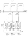
- the second embodiment of the present invention involves connecting the above-described sequence controller to assembling apparatus.
- the second embodiment comprises a first, a second and a third controller system, the first controller system having three I/O modules 3 connected to a CPU module 2, the second controller system having four I/O modules 3 connected to a CPU module 4, the third controller system having two I/O modules 3 connected to a CPU module 6.
- the CPU module 2 controls an assembling apparatus A via the three I/O modules A, B and C.
- the CPU module 4 controls an assembling apparatus B via the four I/O modules D, E, F and G.
- the CPU module 6 controls an assembling apparatus C via the two I/O modules H and I. Parts to be assembled are conveyed on an assembly line 80 past the assembling apparatus A, B and C, in that order, the apparatus performing the respectively assigned assembly processes. Coordinated operation is required between the assembling apparatus A and B and also between the assembling apparatus B and C.
- the CPU module 2 exchanges data with the I/O modules A, B and C; the CPU module 4 exchanges data with the I/O modules D, E, F and G; and the CPU module 6 exchanges data with the I/O modules H and I.
- the CPU modules each control the assembling apparatus A, B and C independently.
- the data exchanges made through I/O modules in the comparable prior art setup are replaced in the second embodiment with those between the CPU modules 1 and 2 and between the CPU modules 2 and 3.
- data is exchanged direct between CPU modules in the second embodiment. This means that there is no need for those I/O modules together with the wiring therebetween which are required for the data exchanges in the prior art setup.
- Fig. 9 depicts the range of I/O data transfer carried out by the CPU modules 2, 4 and 6 in the embodiment of Fig. 8.
- the CPU module 2 performs I/O data transfer across the I/O modules A through C to the CPU module 4.
- the I/O modules A through C constitute a controller for the assembling apparatus A.
- the CPU module 2 exchanges data with the CPU module 4 to provide coordinated control between the first and the second controller systems.
- the CPU module 4 carries out data transfer across the I/O modules D through G to the CPU module 6.
- the I/O modules G through G under the CPU module 4 control the assembling apparatus B, and the CPU module 4 exchanges data with the CPU module 6.
- the CPU module G performs data transfer to the I/O modules H and I alone and controls the assembling apparatus C.
- the CPU module 4 e.g., transferring data from the CPU module 2 to 4 to 6 or from the CPU module 6 to 4 to 2.
- direct data exchange between the CPU modules 2 and 6 is made possible by use of a certain CPU module arrangement to be described later.
- the signal lines 8 on the mother board 30 are compartmentalized to each CPU module so as to form an independently operating controller system centering on each CPU. These independent controller systems operate asynchronously with one another, as illustrated in Fig. 10.
- each CPU that runs independently transfers data not only to the I/O modules but also to the CPU modules located to the right. This permits immediate, direct data exchange between CPU modules with minimum delays of data transmission.
- Fig. 11 gives a magnified view of the CPU module 4 for explanation purposes.
- the CPU module 4 contains a memory 9 in which to store the data of the I/O modules located to the right.
- the CPU module 4 places in the memory 9 the data to be transferred to the I/O modules D, E, F and G.
- the CPU module 2 to the left starts transferring the data to the I/O modules A, B and C, in that order.
- the CPU module 4 then performs its data transfer for subsequent data exchange.
- the next address lines enable memory areas 9a, 9b, 9c, 9d and 9e in the CPU module 4 to be selected, the areas containing the I/O data.
- This allows the CPU module 2 to carry out data transfer apparently direct to each of the memory areas corresponding to the I/O modules D, E, F and G. Therefore, each CPU module may transfer data to all I/O modules and CPU modules located to the right thereof. This feature significantly expands the scope of the sequence controller in functionality.
- each system is allowed to operate independently. Because the power supply module of each system may be shared and because of the absence of the need for specialized I/O modules for data transfer between systems, the scope of the systems is made smaller, and the cost thereof is reduced correspondingly.
- the present invention proposes having one module in a system equipped with a buffer that stores the data to be transferred between the systems. Because data is transferred direct between the systems via this buffer, there is no need for dedicated I/O modules or specialized communication modules.
- This scheme provides a small-sized, low-priced sequence controller that provides high-speed control.
Landscapes
- Physics & Mathematics (AREA)
- General Physics & Mathematics (AREA)
- Engineering & Computer Science (AREA)
- Automation & Control Theory (AREA)
- Programmable Controllers (AREA)
Abstract
Un système de contrôleurs de séquence une pluralité de modules de traitement centraux et de modules d'E/S. Un premier système contrôleur comprend un premier module de traitement central et au moins un premier module d'E/S connecté au premier module de traitement central, et un deuxième système contrôleur comprend un deuxième module de traitement central. Un de ces modules comprend une mémoire tampon de stockage des données transférées entre le premier système contrôleur et le deuxième système contrôleur, cette mémoire tampon étant commandée de façon à effectuer et à arrêter le transfert de données entre le premier système contrôleur et le deuxième système contrôleur. On peut ainsi former une pluralité de systèmes en utilisant les modules de traitement centraux comme des divisions. Chaque module de traitement central fonctionne comme un contrôleur indépendant, effectue l'échange de données avec d'autres modules de traitement centraux en même temps que le transfert de données d'E/S et permet ainsi d'améliorer la vitesse de l'échange de données.
Applications Claiming Priority (3)
| Application Number | Priority Date | Filing Date | Title |
|---|---|---|---|
| JP12880489 | 1989-05-24 | ||
| JP128804/89 | 1989-05-24 | ||
| PCT/JP1990/000662 WO1990014621A1 (fr) | 1989-05-24 | 1990-05-24 | Systeme de controleurs de sequence |
Publications (2)
| Publication Number | Publication Date |
|---|---|
| EP0471846A1 true EP0471846A1 (fr) | 1992-02-26 |
| EP0471846A4 EP0471846A4 (en) | 1994-09-21 |
Family
ID=14993838
Family Applications (1)
| Application Number | Title | Priority Date | Filing Date |
|---|---|---|---|
| EP19900907501 Withdrawn EP0471846A4 (en) | 1989-05-24 | 1990-05-24 | Sequence controller system |
Country Status (2)
| Country | Link |
|---|---|
| EP (1) | EP0471846A4 (fr) |
| WO (1) | WO1990014621A1 (fr) |
Cited By (5)
| Publication number | Priority date | Publication date | Assignee | Title |
|---|---|---|---|---|
| DE9309070U1 (de) * | 1993-06-17 | 1993-08-05 | Siemens AG, 80333 München | Baugruppe für ein elektrisches Gerät |
| US5495421A (en) * | 1991-12-31 | 1996-02-27 | Hadewe B.V. | Method for controlling an apparatus for preparing items to be mailed, and apparatus and auxiliary equipment for carrying out such method |
| US5504671A (en) * | 1992-12-18 | 1996-04-02 | Nokia Telecommunications | Radio system combiner filter control system wherein plural auxiliary cards automatically obtain correct address from motherboard upon being inserted in respective auxiliary card connectors |
| EP0871098A1 (fr) * | 1997-03-11 | 1998-10-14 | SINCROTRONE TRIESTE Societa Consortile per Azioni | Technique d'automatisation et de commande d'unités opératives |
| WO2020256644A1 (fr) * | 2019-06-19 | 2020-12-24 | Amibit D.O.O. | Dispositif de commande modulaire pour différents signaux d'entrée, procédé d'assemblage dudit dispositif de commande et procédé de gestion d'énergie utilisant ledit dispositif de commande |
Families Citing this family (2)
| Publication number | Priority date | Publication date | Assignee | Title |
|---|---|---|---|---|
| JP3329498B2 (ja) * | 1992-12-07 | 2002-09-30 | 横河電機株式会社 | ビルディングブロック形電子機器 |
| US6235273B1 (en) * | 2000-02-03 | 2001-05-22 | Mattel, Inc. | Washable non-toxic body paint for applying color to human skin |
Family Cites Families (4)
| Publication number | Priority date | Publication date | Assignee | Title |
|---|---|---|---|---|
| JPS5884307A (ja) * | 1981-11-16 | 1983-05-20 | Toshiba Mach Co Ltd | プログラマブルシ−ケンスコントロ−ラ |
| JPS6010307U (ja) * | 1983-06-30 | 1985-01-24 | 株式会社東芝 | プロセス制御装置 |
| JPS63113603A (ja) * | 1986-10-30 | 1988-05-18 | Yaskawa Electric Mfg Co Ltd | 複数のプログラマブルコントロ−ラの接続方式 |
| JPS63268004A (ja) * | 1987-04-24 | 1988-11-04 | Koyo Denshi Kogyo Kk | プログラマブル・コントロ−ラ |
-
1990
- 1990-05-24 EP EP19900907501 patent/EP0471846A4/en not_active Withdrawn
- 1990-05-24 WO PCT/JP1990/000662 patent/WO1990014621A1/fr not_active Ceased
Non-Patent Citations (2)
| Title |
|---|
| No further relevant documents disclosed * |
| See also references of WO9014621A1 * |
Cited By (6)
| Publication number | Priority date | Publication date | Assignee | Title |
|---|---|---|---|---|
| US5495421A (en) * | 1991-12-31 | 1996-02-27 | Hadewe B.V. | Method for controlling an apparatus for preparing items to be mailed, and apparatus and auxiliary equipment for carrying out such method |
| US5504671A (en) * | 1992-12-18 | 1996-04-02 | Nokia Telecommunications | Radio system combiner filter control system wherein plural auxiliary cards automatically obtain correct address from motherboard upon being inserted in respective auxiliary card connectors |
| DE9309070U1 (de) * | 1993-06-17 | 1993-08-05 | Siemens AG, 80333 München | Baugruppe für ein elektrisches Gerät |
| EP0871098A1 (fr) * | 1997-03-11 | 1998-10-14 | SINCROTRONE TRIESTE Societa Consortile per Azioni | Technique d'automatisation et de commande d'unités opératives |
| WO2020256644A1 (fr) * | 2019-06-19 | 2020-12-24 | Amibit D.O.O. | Dispositif de commande modulaire pour différents signaux d'entrée, procédé d'assemblage dudit dispositif de commande et procédé de gestion d'énergie utilisant ledit dispositif de commande |
| US20220317642A1 (en) * | 2019-06-19 | 2022-10-06 | Amibit D.O.O. | A modular controller for different input signals, an assembly method of the said controller and a method for energy management using the said controller |
Also Published As
| Publication number | Publication date |
|---|---|
| EP0471846A4 (en) | 1994-09-21 |
| WO1990014621A1 (fr) | 1990-11-29 |
Similar Documents
| Publication | Publication Date | Title |
|---|---|---|
| US4691296A (en) | Method and apparatus for exchanging multiple data bytes with an I/O module in a single scan. | |
| US4443866A (en) | Automatic device selection circuit | |
| EP1988435B1 (fr) | Commande à programme mémorisé modulaire | |
| EP0117954A2 (fr) | Réseaux à bus pour systèmes de traitement de données numériques et modules utilisables dans de tels systèmes | |
| JPH04320509A (ja) | 並列処理装置 | |
| JPH05155632A (ja) | ガラス製品形成マシンのための電子的タイミングシステム | |
| EP0471846A1 (fr) | Systeme de controleurs de sequence | |
| US4126897A (en) | Request forwarding system | |
| US4050098A (en) | Self-addressing modules for programmable controller | |
| CN101261506B (zh) | 组块式可编程逻辑控制器 | |
| US5107257A (en) | Bus relay apparatus for multi-data communication processing system | |
| EP0055301A1 (fr) | Unite de commande numerique | |
| US6537109B1 (en) | Chainable I/O termination block system | |
| US5564059A (en) | Simplified protocol for expanding a fixed width bus in an industrial controller | |
| US20130132623A1 (en) | Method for Interconnecting Modules for High Speed Bidirectional Communications | |
| US4942573A (en) | Loosely coupled parallel network simulator | |
| JPWO1990014621A1 (ja) | シーケンスコントローラシステム | |
| JPS60207918A (ja) | プログラマブルコントロ−ラ | |
| EP0797134B1 (fr) | Unites d'e/s et tableau de commande pour controleurs numeriques | |
| JPH052570A (ja) | クロスバースイツチおよびそれを使用した並列処理装置 | |
| US4015244A (en) | Selective addressing system | |
| JPH04283B2 (fr) | ||
| JPS61107453A (ja) | モジユ−ルアドレス設定回路 | |
| KR0156390B1 (ko) | 멀티플 메모리를 사용한 고속 전송 인터페이스 회로 | |
| KR100320563B1 (ko) | 메모리 및 입출력 포트 인터페이스 제어 장치 |
Legal Events
| Date | Code | Title | Description |
|---|---|---|---|
| PUAI | Public reference made under article 153(3) epc to a published international application that has entered the european phase |
Free format text: ORIGINAL CODE: 0009012 |
|
| 17P | Request for examination filed |
Effective date: 19911128 |
|
| AK | Designated contracting states |
Kind code of ref document: A1 Designated state(s): DE FR GB IT NL |
|
| RHK1 | Main classification (correction) |
Ipc: G05B 19/04 |
|
| A4 | Supplementary search report drawn up and despatched |
Effective date: 19940729 |
|
| AK | Designated contracting states |
Kind code of ref document: A4 Designated state(s): DE FR GB IT NL |
|
| STAA | Information on the status of an ep patent application or granted ep patent |
Free format text: STATUS: THE APPLICATION IS DEEMED TO BE WITHDRAWN |
|
| 18D | Application deemed to be withdrawn |
Effective date: 19941126 |