EP0473352A2 - Circuit de sortie émetteur-suiveur - Google Patents
Circuit de sortie émetteur-suiveur Download PDFInfo
- Publication number
- EP0473352A2 EP0473352A2 EP91307672A EP91307672A EP0473352A2 EP 0473352 A2 EP0473352 A2 EP 0473352A2 EP 91307672 A EP91307672 A EP 91307672A EP 91307672 A EP91307672 A EP 91307672A EP 0473352 A2 EP0473352 A2 EP 0473352A2
- Authority
- EP
- European Patent Office
- Prior art keywords
- bipolar transistor
- collector
- npn bipolar
- potential
- base
- Prior art date
- Legal status (The legal status is an assumption and is not a legal conclusion. Google has not performed a legal analysis and makes no representation as to the accuracy of the status listed.)
- Granted
Links
- 230000008859 change Effects 0.000 claims abstract description 5
- 239000003990 capacitor Substances 0.000 abstract description 7
- 238000010586 diagram Methods 0.000 description 10
- 230000000694 effects Effects 0.000 description 5
- 230000007704 transition Effects 0.000 description 3
- 238000007599 discharging Methods 0.000 description 2
- 230000004044 response Effects 0.000 description 2
- 235000001537 Ribes X gardonianum Nutrition 0.000 description 1
- 235000001535 Ribes X utile Nutrition 0.000 description 1
- 235000016919 Ribes petraeum Nutrition 0.000 description 1
- 244000281247 Ribes rubrum Species 0.000 description 1
- 235000002355 Ribes spicatum Nutrition 0.000 description 1
- 230000003321 amplification Effects 0.000 description 1
- 230000008878 coupling Effects 0.000 description 1
- 238000010168 coupling process Methods 0.000 description 1
- 238000005859 coupling reaction Methods 0.000 description 1
- 230000007423 decrease Effects 0.000 description 1
- 230000002542 deteriorative effect Effects 0.000 description 1
- 238000003199 nucleic acid amplification method Methods 0.000 description 1
- 230000000630 rising effect Effects 0.000 description 1
- 229920006395 saturated elastomer Polymers 0.000 description 1
Images



Classifications
-
- H—ELECTRICITY
- H03—ELECTRONIC CIRCUITRY
- H03K—PULSE TECHNIQUE
- H03K19/00—Logic circuits, i.e. having at least two inputs acting on one output; Inverting circuits
- H03K19/01—Modifications for accelerating switching
- H03K19/013—Modifications for accelerating switching in bipolar transistor circuits
- H03K19/0136—Modifications for accelerating switching in bipolar transistor circuits by means of a pull-up or down element
Definitions
- an emitter follower circuit of this kind is often used as an output circuit connected to the output side of a differential logic circuit constituted by a pair of differential transistors, so as to drive a load connected to a next stage.
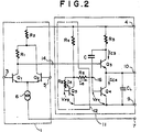
- the NPN bipolar transistor Q1 when a signal applied to the input terminal 3 has a high level potential, the NPN bipolar transistor Q1 becomes conductive, while the NPN bipolar transistor Q2 becomes non-conductive.
- the base bias circuit 12 is constituted by three resistors R4, R5 and R6 and an NPN bipolar transistor Q5.
- the relation similar to the equation (2) is established between the collector current and the base-emitter voltage, so that the collector current of the transistor becomes lower than the current value in the steady-state described above.
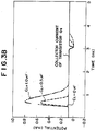
- the collector current of the NPN bipolar transistor Q4 flows through the output NPN bipolar transistor Q3, the potential at the base of the NPN bipolar transistor Q4 returns to the constant potential given by the base bias circuit 12, and the potential at the collector of the NPN bipolar transistor Q3 and the collector current of the NPN bipolar transistor Q4 return to steady-state values as shown in Figs. 3A and 3B, respectively.
- the operation conditions of the embodiment are as follows.
Landscapes
- Physics & Mathematics (AREA)
- Engineering & Computer Science (AREA)
- Computer Hardware Design (AREA)
- Computing Systems (AREA)
- General Engineering & Computer Science (AREA)
- Mathematical Physics (AREA)
- Logic Circuits (AREA)
Applications Claiming Priority (2)
| Application Number | Priority Date | Filing Date | Title |
|---|---|---|---|
| JP2220203A JPH04103218A (ja) | 1990-08-22 | 1990-08-22 | エミッタフォロア出力回路 |
| JP220203/90 | 1990-08-22 |
Publications (3)
| Publication Number | Publication Date |
|---|---|
| EP0473352A2 true EP0473352A2 (fr) | 1992-03-04 |
| EP0473352A3 EP0473352A3 (en) | 1992-08-05 |
| EP0473352B1 EP0473352B1 (fr) | 1998-02-04 |
Family
ID=16747505
Family Applications (1)
| Application Number | Title | Priority Date | Filing Date |
|---|---|---|---|
| EP91307672A Expired - Lifetime EP0473352B1 (fr) | 1990-08-22 | 1991-08-21 | Circuit de sortie émetteur-suiveur |
Country Status (4)
| Country | Link |
|---|---|
| US (1) | US5233234A (fr) |
| EP (1) | EP0473352B1 (fr) |
| JP (1) | JPH04103218A (fr) |
| DE (1) | DE69128856T2 (fr) |
Cited By (1)
| Publication number | Priority date | Publication date | Assignee | Title |
|---|---|---|---|---|
| EP1047194A1 (fr) * | 1999-04-23 | 2000-10-25 | STMicroelectronics S.r.l. | Etage d' ecrétage à haute fréquence |
Families Citing this family (2)
| Publication number | Priority date | Publication date | Assignee | Title |
|---|---|---|---|---|
| US20030185204A1 (en) * | 2002-04-01 | 2003-10-02 | Murdock Scott D. | Data communication system combining pay telephone and wireless access technologies |
| US9425748B2 (en) | 2014-05-20 | 2016-08-23 | Freescale Semiconductor, Inc. | Amplifier circuit, bi-stage amplifier circuit, multi-stage amplifier circuit, RF-amplifier circuit, receiver section, RF-transceiver, and integrated circuit |
Family Cites Families (12)
| Publication number | Priority date | Publication date | Assignee | Title |
|---|---|---|---|---|
| BE644317A (fr) * | 1963-02-25 | |||
| US4331887A (en) * | 1980-06-23 | 1982-05-25 | International Business Machines Corporation | Current switch driving circuit arrangements |
| US4623803A (en) * | 1983-11-08 | 1986-11-18 | Advanced Micro Devices, Inc. | Logic level translator circuit for integrated circuit semiconductor devices having transistor-transistor logic output circuitry |
| US4683383A (en) * | 1984-07-19 | 1987-07-28 | Tandem Computers Incorporated | Driver circuit for a three-state gate array using low driving current |
| US4672242A (en) * | 1986-03-06 | 1987-06-09 | Advanced Micro Devices, Inc. | Reduced power/temperature controlled TTL tri-state buffer utilizing three phase splitter transistors |
| JPS6444610A (en) * | 1987-08-12 | 1989-02-17 | Toshiba Corp | Output circuit |
| US4926065A (en) * | 1987-11-17 | 1990-05-15 | Applied Micro Circuits Corporation | Method and apparatus for coupling an ECL output signal using a clamped capacitive bootstrap circuit |
| JPH01190021A (ja) * | 1988-01-25 | 1989-07-31 | Sharp Corp | パルス増幅回路 |
| US4835455A (en) * | 1988-09-15 | 1989-05-30 | Honeywell Inc. | Reference voltage generator |
| FR2641143A1 (en) * | 1988-12-27 | 1990-06-29 | Thomson Composants Militaires | Output buffer amplifier in bipolar technology |
| KR930009491B1 (ko) * | 1989-09-18 | 1993-10-04 | 후지쓰 가부시끼가이샤 | Ecl회로 |
| US5059827A (en) * | 1990-07-31 | 1991-10-22 | Motorola, Inc. | ECL circuit with low voltage/fast pull-down |
-
1990
- 1990-08-22 JP JP2220203A patent/JPH04103218A/ja active Pending
-
1991
- 1991-08-21 EP EP91307672A patent/EP0473352B1/fr not_active Expired - Lifetime
- 1991-08-21 DE DE69128856T patent/DE69128856T2/de not_active Expired - Fee Related
- 1991-08-22 US US07/748,622 patent/US5233234A/en not_active Expired - Fee Related
Cited By (1)
| Publication number | Priority date | Publication date | Assignee | Title |
|---|---|---|---|---|
| EP1047194A1 (fr) * | 1999-04-23 | 2000-10-25 | STMicroelectronics S.r.l. | Etage d' ecrétage à haute fréquence |
Also Published As
| Publication number | Publication date |
|---|---|
| JPH04103218A (ja) | 1992-04-06 |
| EP0473352A3 (en) | 1992-08-05 |
| DE69128856T2 (de) | 1998-07-30 |
| US5233234A (en) | 1993-08-03 |
| EP0473352B1 (fr) | 1998-02-04 |
| DE69128856D1 (de) | 1998-03-12 |
Similar Documents
| Publication | Publication Date | Title |
|---|---|---|
| EP0177278A1 (fr) | Circuit logique à émetteurs couplés | |
| JPH0332026B2 (fr) | ||
| KR960016010B1 (ko) | 지연-펄스 발생기 | |
| EP0432577A1 (fr) | Circuit ECL | |
| EP0219937A2 (fr) | Générateurs asservis de référence pour ECL | |
| JPH0554689A (ja) | サンプルホールド回路およびバツフア回路およびそれらを用いたサンプルホールド装置 | |
| US4503339A (en) | Semiconductor integrated circuit device having a substrate voltage generating circuit | |
| EP0473352B1 (fr) | Circuit de sortie émetteur-suiveur | |
| EP0435335B1 (fr) | Circuit de transistor et circuit convertisseur de niveau | |
| US4567380A (en) | Schmitt trigger circuit | |
| JPH01130616A (ja) | シュミットトリガ回路 | |
| KR100646026B1 (ko) | 넓은 주파수범위를 가지는 srpp회로 | |
| JPS61293022A (ja) | Ecl−ttl変換出力回路 | |
| US4501974A (en) | Pulse stretching and level shifting circuit | |
| US4140926A (en) | Inverted transistor circuits for monolithic integrated circuit application | |
| US4627081A (en) | Shift register stage | |
| US3470486A (en) | Differential amplifier single ending circuit | |
| EP0465167A2 (fr) | Circuit logique sans seuil | |
| JPH0744401B2 (ja) | フローティング電源アンプ | |
| EP0340725A2 (fr) | Circuit de conversion de niveau ECL-TTL | |
| EP0645687A2 (fr) | Circuit de génération d'une tension de référence | |
| KR900006711Y1 (ko) | 트리거 펄스의 안정화 회로 | |
| JPH04253421A (ja) | Ecl回路 | |
| JPH0728187B2 (ja) | 差動増幅回路 | |
| JPH07154167A (ja) | エミッタホロワ出力電流制限回路 |
Legal Events
| Date | Code | Title | Description |
|---|---|---|---|
| PUAI | Public reference made under article 153(3) epc to a published international application that has entered the european phase |
Free format text: ORIGINAL CODE: 0009012 |
|
| 17P | Request for examination filed |
Effective date: 19910905 |
|
| AK | Designated contracting states |
Kind code of ref document: A2 Designated state(s): DE FR GB |
|
| PUAL | Search report despatched |
Free format text: ORIGINAL CODE: 0009013 |
|
| AK | Designated contracting states |
Kind code of ref document: A3 Designated state(s): DE FR GB |
|
| 17Q | First examination report despatched |
Effective date: 19951010 |
|
| GRAG | Despatch of communication of intention to grant |
Free format text: ORIGINAL CODE: EPIDOS AGRA |
|
| GRAG | Despatch of communication of intention to grant |
Free format text: ORIGINAL CODE: EPIDOS AGRA |
|
| GRAH | Despatch of communication of intention to grant a patent |
Free format text: ORIGINAL CODE: EPIDOS IGRA |
|
| GRAH | Despatch of communication of intention to grant a patent |
Free format text: ORIGINAL CODE: EPIDOS IGRA |
|
| GRAA | (expected) grant |
Free format text: ORIGINAL CODE: 0009210 |
|
| AK | Designated contracting states |
Kind code of ref document: B1 Designated state(s): DE FR GB |
|
| REF | Corresponds to: |
Ref document number: 69128856 Country of ref document: DE Date of ref document: 19980312 |
|
| ET | Fr: translation filed | ||
| PLBE | No opposition filed within time limit |
Free format text: ORIGINAL CODE: 0009261 |
|
| STAA | Information on the status of an ep patent application or granted ep patent |
Free format text: STATUS: NO OPPOSITION FILED WITHIN TIME LIMIT |
|
| 26N | No opposition filed | ||
| PGFP | Annual fee paid to national office [announced via postgrant information from national office to epo] |
Ref country code: FR Payment date: 20010810 Year of fee payment: 11 |
|
| PGFP | Annual fee paid to national office [announced via postgrant information from national office to epo] |
Ref country code: DE Payment date: 20010813 Year of fee payment: 11 |
|
| PGFP | Annual fee paid to national office [announced via postgrant information from national office to epo] |
Ref country code: GB Payment date: 20010815 Year of fee payment: 11 |
|
| REG | Reference to a national code |
Ref country code: GB Ref legal event code: IF02 |
|
| PG25 | Lapsed in a contracting state [announced via postgrant information from national office to epo] |
Ref country code: GB Free format text: LAPSE BECAUSE OF NON-PAYMENT OF DUE FEES Effective date: 20020821 |
|
| PG25 | Lapsed in a contracting state [announced via postgrant information from national office to epo] |
Ref country code: DE Free format text: LAPSE BECAUSE OF NON-PAYMENT OF DUE FEES Effective date: 20030301 |
|
| GBPC | Gb: european patent ceased through non-payment of renewal fee |
Effective date: 20020821 |
|
| PG25 | Lapsed in a contracting state [announced via postgrant information from national office to epo] |
Ref country code: FR Free format text: LAPSE BECAUSE OF NON-PAYMENT OF DUE FEES Effective date: 20030430 |
|
| REG | Reference to a national code |
Ref country code: FR Ref legal event code: ST |