EP0473420A2 - Virtuelle Langebefehlswortspeicherarchitektur für digitalen Signalprozessor - Google Patents
Virtuelle Langebefehlswortspeicherarchitektur für digitalen Signalprozessor Download PDFInfo
- Publication number
- EP0473420A2 EP0473420A2 EP91307890A EP91307890A EP0473420A2 EP 0473420 A2 EP0473420 A2 EP 0473420A2 EP 91307890 A EP91307890 A EP 91307890A EP 91307890 A EP91307890 A EP 91307890A EP 0473420 A2 EP0473420 A2 EP 0473420A2
- Authority
- EP
- European Patent Office
- Prior art keywords
- instructions
- instruction
- pair
- sequentially adjacent
- instruction word
- Prior art date
- Legal status (The legal status is an assumption and is not a legal conclusion. Google has not performed a legal analysis and makes no representation as to the accuracy of the status listed.)
- Withdrawn
Links
Images

Classifications
-
- G—PHYSICS
- G06—COMPUTING OR CALCULATING; COUNTING
- G06F—ELECTRIC DIGITAL DATA PROCESSING
- G06F9/00—Arrangements for program control, e.g. control units
- G06F9/06—Arrangements for program control, e.g. control units using stored programs, i.e. using an internal store of processing equipment to receive or retain programs
- G06F9/30—Arrangements for executing machine instructions, e.g. instruction decode
- G06F9/38—Concurrent instruction execution, e.g. pipeline or look ahead
- G06F9/3885—Concurrent instruction execution, e.g. pipeline or look ahead using a plurality of independent parallel functional units
- G06F9/3889—Concurrent instruction execution, e.g. pipeline or look ahead using a plurality of independent parallel functional units controlled by multiple instructions, e.g. MIMD, decoupled access or execute
-
- G—PHYSICS
- G06—COMPUTING OR CALCULATING; COUNTING
- G06F—ELECTRIC DIGITAL DATA PROCESSING
- G06F9/00—Arrangements for program control, e.g. control units
- G06F9/06—Arrangements for program control, e.g. control units using stored programs, i.e. using an internal store of processing equipment to receive or retain programs
- G06F9/30—Arrangements for executing machine instructions, e.g. instruction decode
- G06F9/34—Addressing or accessing the instruction operand or the result ; Formation of operand address; Addressing modes
-
- G—PHYSICS
- G06—COMPUTING OR CALCULATING; COUNTING
- G06F—ELECTRIC DIGITAL DATA PROCESSING
- G06F9/00—Arrangements for program control, e.g. control units
- G06F9/06—Arrangements for program control, e.g. control units using stored programs, i.e. using an internal store of processing equipment to receive or retain programs
- G06F9/30—Arrangements for executing machine instructions, e.g. instruction decode
- G06F9/38—Concurrent instruction execution, e.g. pipeline or look ahead
- G06F9/3885—Concurrent instruction execution, e.g. pipeline or look ahead using a plurality of independent parallel functional units
Definitions
- the present invention relates generally to digital signal processors and particularly to methods and systems for providing or generating long instruction words, which are efficient for high speed processing, while using a short word instruction memory.
- program instructions can generally be divided into load/store instructions, which load values from the processor's random access memory into the processor's registers or store back register values into memory, and arithmetic instructions, which perform mathematical computations. While the mathematical computations make use of the processor's registers, the digital signal processor of the present invention takes advantage of the fact that a load/store instruction can be performed simultaneously with an arithmetic instruction.
- the present invention forms long instruction words from sequences of shorter instruction words when combining such sequences of shorting instruction words into a single instruction comprises an allowed combination, as determined by a set of predefined rules.
- Short instructions each perform only a load/store or only an arithmetic operation.
- a long instructions is a combination of a load/store instruction and an arithmetic instruction. Long instructions can also be applied to implement two-word instructions in one machine cycle.
- the present invention allows the system to store short instruction words in external program memory, which is efficient for memory storage purposes, and to dynamically combine short instructions into long instructions, which is efficient for executing programs.
- the present invention is an instruction memory apparatus for a data processing unit.
- An instruction memory stores a sequence of instructions. At each instruction fetch cycle, two sequentially adjacent instructions are accessed.
- An instruction preprocessing unit coupled to the instruction memory, combines the two sequentially adjacent instructions into a single long instruction word when the two instructions meet predefined criteria for being combined. The first of the two adjacent instructions is combined with a no-operation instruction to generate a long instruction word when the predefined criteria are not met. In that case, the second instruction may be accessed again during the next instruction fetch cycle as the first of two adjacent instructions.
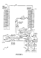
- Figure 1 is a block diagram of a digital signal processor with an instruction memory buffer and an instruction preprocessing unit.
- Figure 2 is a conceptual block diagram of an instruction memory buffer for generating and storing long instruction words.
- Figure 3 is a block diagram of a first preferred embodiment of the present invention.
- Figure 4 is a block diagram of a second preferred embodiment of the present invention.
- Figure 5 is a block diagram of a memory buffer suitable for implementing the memory buffer portion of the present invention.
- Figure 6 is a block diagram of a third preferred embodiment of the present invention.
- a data processing system 100 having a digital signal processor (DSP) 102 coupled to a program memory 104.
- the program memory 104 is typically random access memory (RAM) or read only memory (ROM), although other types of memory systems may be used.
- the DSP 102 fetches program instructions from the program memory and temporarily stores those instructions in a memory buffer 110 which is used as a memory cache.
- the memory buffer 110 may have a storage capacity of 512 instruction words, each of which is thirty-two bits long. The exact mechanism and timing control used for loading data into the internal memory buffer 110 may vary from implementation to implementation.
- the basic principal used in the present invention is that a long instruction word (e.g., 60 to 64 bits) is used internal to the DSP 102, because it allows a high degree of orthogonality and parallelism in the instruction set, but the program memory 104 stores shorter instruction words (e.g., 32 bits long) because a 32-bit wide program memory 104 and a 32-bit wide interface between the DSP 102 and the program memory are much less expensive than they would be for a 64-bit wide program memory.
- An instruction preprocessing unit 112 is used to convert pairs of short instruction words into long instruction words, and then deliver them to the DSP's instruction decoders 114 and 116.
- the DSP 102 has two instruction decoders 114 and 116.
- the first instruction decoder 114 is used to decode register load and store instructions, which are instructions used to load values from a random access memory 124 into the processor's registers 120 or to store back values from registers 120 to memory 124.
- the second instruction decoder 116 decodes arithmetic and execution control instructions, which are executed by the DSP's arithmetic logic unit 122 to perform mathematical computations, including multiplication and accumulation operations. Arithmetic and execution control instructions are herein collectively called arithmetic instructions, and the hardware circuits for processing these instructions are labelled EXEC in the Figures.
- the use of parallel instruction decoders 114-116 takes advantage of the fact that a load/store instruction can be performed simultaneously with an arithmetic instruction.
- the registers used in the DSP 102 are master-slave type registers, which allows the DSP to simultaneously read previously loaded data and to write new data into a register without any interference between the two simultaneous operations. Therefore when a long instruction has a load/store operation and an arithmetic operation, both of which use the same register(s); the arithmetic operation uses the value previously loaded into the register(s) while the load/store operation loads a new value into the very same register(s).
- the internal program buffer 110 has two columns 126 and 128, column 126 being used to store arithmetic instructions and column 128 being used to store load/store instructions.
- Each thirty-two bit instruction 130 in the program memory 104 contains a one-bit instruction identifier IID 132, and a thirty-one bit instruction code 134. IID equals zero (0) for arithmetic instructions, and it equals one (1) for load/store instructions.
- An instruction input demultiplexer 140 controlled by the IID bit from each instruction, switches the remaining thirty-one bit instruction code into either the arithmetic instruction column 126 or the load/store column 128 of the internal program buffer 110.
- both instructions are loaded into a single column of the internal memory buffer 110, thereby combining the two instructions into a single long instruction word. If the two sequentially fetched instructions are not compatible, then the are loaded into separate columns and a "NOP" (i.e., no-operation) instruction is loaded into the unused slot of one of the columns.
- NOP i.e., no-operation
- the predefined compatibility rule in the first preferred embodiment of the present invention is as follows: If an arithmetic instruction is followed by a load/store instruction, the two are combined into a single long instruction word by placing the load/store instruction along side the arithmetic instruction. If one execute instruction immediately follows another arithmetic instruction, the corresponding load/store field for the first arithmetic instruction is filled with a NOP, and the second arithmetic instruction is stored in the next row of the internal program buffer. The same is true for two or more load/store instructions in a sequence: a NOP will be placed in the arithmetic instruction fields of the load/store instructions that cannot be combined with an arithmetic instruction.
- the predefined compatibility rule is the opposite of that in the first preferred embodiment: If a load/store instruction is followed by an arithmetic instruction, the two are combined into a single long instruction word by placing the load/store instruction along side the arithmetic instruction.
- a load/store instruction is followed by an arithmetic instruction
- the two are combined into a single long instruction word by placing the load/store instruction along side the arithmetic instruction.
- Other implementations of the invention might combine an arithmetic instruction with a load/store instruction regardless of the order in which they occur in the program.
- a DSP 102 that fetches and executes program instructions directly from a program memory has a maximum execution speed of one instruction per fetch cycle.
- an arithmetic and a load/store instruction can be executed simultaneously, thereby yielding two times the performance of the DSP which uses only a program memory.
- the programmer, or program compiler must schedule the instruction sequence so that arithmetic and load/store instructions are interleaved. Such interleaving allows arithmetic and load/store instructions to be executed in parallel. If such interleaving cannot be used, the program will still execute correctly, but the DSP's resources will by under utilized.
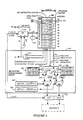
- FIG. 3 there is shown a preferred embodiment of the internal instruction memory buffer 110 and one version of an instruction preprocessing unit 150 for combining sequentially accessed instructions when those instructions are deemed to be compatible.
- This circuit 150 splits a serial stream of 32-bit wide instructions into two paths so as to generate a sequence of 62-bit wide parallel instructions.
- each fetch cycle is split into an EXEC phase and a LD/ST phase.
- the two instructions are simultaneously loaded into a pipeline register 186 for transmission to the DSP's instruction decoders 114, 116.
- a NOP instruction is loaded with the first (arithmetic) instruction into the pipeline register 186, and the program counter 154 is not incremented at the beginning of the next EXEC clock phase.
- the first instruction accessed during the EXEC clock phase was a load/store instruction, it is loaded with a NOP instruction into the pipeline register and the program counter 154 is not incremented until the beginning of the next EXEC clock phase.
- the circuit 150 works as follows.
- the instruction preprocessor 150 uses a clock signal on line 152 which runs at twice the instruction fetch rate.
- the clock signal on line 152 increments the program counter 154 when the clock signal is passed by AND gate 156.
- the clock signal is divided down by a flip-flop circuit 160 to generate two complementary clock signals: a LD/ST (i.e., load/store) phase signal on line 162 and an EXEC phase signal on line 164.
- a LD/ST i.e., load/store
- EXEC phase signal on line 164 an instruction fetch cycle (comprising two clock cycles of the clock signal on line 152) has two phases: an EXEC phase during which the EXEC phase signal on line 164 is enabled (i.e., high), and a LD/ST phase during which the LD/ST phase clock signal on line 162 is enabled.
- the instruction identifier IID from each accessed instruction is logically ANDed with each of these phase clocks by AND gates 166 and 168.
- AND gate 166 generates an enabled output signal, called EXEC VALID, during the EXEC clock phase if the access instruction has an IID equal to 0, meaning that the accessed instruction is an arithmetic instruction.
- AND gate 168 generates an enabled output signal, called LD/ST VALID, during the load/store clock phase if the access instruction has an IID equal to 1, meaning that the accessed instruction is a load/store instruction.
- the EXEC VALID and LD/ST VALID signals are logically ORed by OR gate 170 to generate a signal called PC CLOCK ENABLE. Whenever the PC CLOCK ENABLE signal is ON, the next pulse of the clock signal on line 152 is passed by AND gate 156, thereby incrementing the program counter PC 154.
- the EXEC VALID signal generated by AND gate 166 determines whether multiplexer 172 loads a NOP instruction or the instruction code on line 174, read from the cache memory buffer 110 during the EXEC phase, into pipeline register 176. If the instruction accessed during the EXEC phase is an arithmetic instruction, this instruction is loaded into pipeline register 176, otherwise a NOP instruction is loaded.
- the LD/ST VALID signal generated by AND gate 168 determines whether multiplexer 180 loads a NOP instruction or the instruction accessed during the LD/ST phase into pipeline register 182. If the instruction accessed during the LD/ST phase is a load/store instruction, this instruction is loaded into pipeline register 182, otherwise a NOP instruction is loaded.
- the instruction codes and/or NOP instructions stored in the pipeline registers 176 and 182 are then loaded into another pipeline register 186, which is used to store the current instruction word as it is being decoded by the DSP's decoders 114 and 116.
- Optimum computational efficiency is achieved by sequencing the program with alternating load/store and arithmetic instructions, but no space is wasted in the program memory 104 (nor in the internal cache memory buffer 110) if the ideal instruction sequence is not achieved.
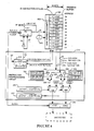
- the internal cache memory 200 has a dual address decoder for simultaneously accessing two instructions (i.e., two rows of data) from the cache.
- Each row 202 of the internal cache memory contains a thirty-bit instruction code 204, and two flags: an instruction identifier IID 206, plus a grouping flag 208.
- the instruction identifier IID 206 in this embodiment has the opposite definition from the one used in the first preferred embodiment.
- IID is equal to 0 for load/store instructions and for the upper word of a long instruction, and is equal to 1 for arithmetic instructions and for the lower word of a long instruction.
- this embodiment envisions three types of instructions: arithmetic instructions, load/store instructions and "long" instructions (i.e., instructions which inherently occupy 60 to 64 bits).
- the instruction preprocessing circuit 210 in this embodiment of the invention works as follows. When two sequentially stored instructions are accessed from the cache 200, if the grouping flags from both instructions are equal, then those two instructions will be combined into a long instruction word. If the grouping flags are not equal, then the instruction accessed from the lower address location (herein called the first address location) is combined with a NOP instruction, in which case the second accessed instruction is used during the next instruction fetch cycle (unless a jump instruction causes the program counter to be reloaded with a new value). Thus, in this embodiment, the order of EXEC and LD/ST instructions is not used to determine whether to combine instructions. Instead, a grouping flag for each instruction is used to explicitly make this determination.
- the two grouping flags are input to an exclusive OR gate 211, to generate a "different line" signal DL.
- DL is enabled if the two grouping flags are unequal (i.e., the two instructions belong on different lines of the program, when using long instruction word format), and is disabled when the two grouping flags are equal.
- the DL signal is also used to determine whether the program counter 214 increments by a count of one or two at the beginning of the next instruction fetch cycle.
- the least significant bit on the address value output by the program counter 214 is inverted to generate a signal herein called the even flag (EF) signal.
- EF is equal to 1 whenever the program counter is pointing to an instruction at an even address.
- a slave unit 215 outputs a value equal to the output of the program counter plus one.
- the two accessed instructions must be preprocessed so as to properly load one or both instructions into a pipeline register 220.
- the idea here is that the control logic 226 for buffers 224 and 228 avoids asserting two load/store instructions simultaneously on line 230 if both accessed instructions are load/store instructions.
- the boolean logic equations shown in Figure 4 for the control logic circuits 226 and 238 are easily implemented using a small number of inverters, NAND and NOR gates.
- Control logic circuits 250 and 252 determine whether multiplexers 222 and 236 pass the instructions on line 230 and 240 or a no-operation (NOP) instruction to pipeline register 220. If the two retrieved instructions have the same grouping flag, making DL equal to 0, then logic circuits 250 and 252 both output a value of "0", causing both multiplexers to pass the retrieved instructions (which are now found on lines 230 and 240) to the pipeline register 220. These instructions are latched into the pipeline register 220 by the clock signal at the beginning of the next instruction fetch cycle.
- NOP no-operation
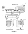
- FIG. 5 there is shown one embodiment of the instruction memory cache 200 for use in conjunction with the embodiment of the invention shown in Figure 4.
- This memory cache 200 has two memory banks 260 and 262, bank 260 being used to store instructions at even address locations and bank 262 being used to store instructions at odd address locations.
- Both program counters are loaded with initial values.
- the master program counter is loaded with a specified value, and the slave program counter uses an increment circuit 268 to increment that value by one before loading it into counter circuit 270. Thereafter, until a new starting address is loaded into the program counters, both counters 264 and 266 are incremented by the same amounts (1 or 2) at the beginning. of each fetch cycle.
- the outputs from the two program counters 264 and 266 are such that two multiplexers 272 and 274 are needed to determine which counter output should go to each memory bank 260, 262.
- Multiplexer 272 sends one of the two count values to memory bank 260 and multiplexer 274 sends the other one of the two count values to memory bank 262.
- the least significant bit (LSB) of the count value output by the master program counter 264 is used to specify which input of each multiplexer 272, 274 is to be used.
- the master program counter 264 is outputting an even value (and the slave counter 266 is outputting an odd value), and therefore the master program count value is used for the even memory bank 260 and the slave program count value is used for the odd memory bank 262. If the LSB is equal to 1, the master program count value is used for the odd memory bank 262 and the slave program count value is used for the odd memory bank 260.
- Table 1 lists an example of a FIR filter program using the present invention.
- Table 1 lists an example of a FIR filter program using the present invention.
- the "number crunching section" of the program makes use of parallel EXEC and LD/ST operations. Since the number crunching section is short, all instructions will be accessed from the memory cache 200, without having to access program memory 104. Furthermore, while the number crunching section is short, it is repeated many times, which makes the parallel processing of arithmetic and load/store instructions effective, even though such parallel processing is used in only a small number of lines of the signal processing program.
- the instruction memory cache 300 includes a one-bit instruction identifier IID 302 for each row, but does not include a grouping flag. This allows the instruction code for each instruction to be thirty-one bits long instead of only thirty bits.
- a special logic circuit 312 which generates the "different line" DL signal based on the even-row instruction identifier EIID, odd-row instruction identifier OIID and even flag EF.
- LD/ST NOP NOP EXEC the programmer must insert a NOP instruction in the program memory between the LD/ST instruction and the EXEC instruction. This means a certain loss in the compression ratio of the stored program to the final executed program, but such instruction sequences requiring the explicit programming of NOP instructions are likely to occur only infrequently.
Landscapes
- Engineering & Computer Science (AREA)
- Software Systems (AREA)
- Theoretical Computer Science (AREA)
- Physics & Mathematics (AREA)
- General Engineering & Computer Science (AREA)
- General Physics & Mathematics (AREA)
- Advance Control (AREA)
- Executing Machine-Instructions (AREA)
Applications Claiming Priority (2)
| Application Number | Priority Date | Filing Date | Title |
|---|---|---|---|
| US575140 | 1990-08-29 | ||
| US07/575,140 US5163139A (en) | 1990-08-29 | 1990-08-29 | Instruction preprocessor for conditionally combining short memory instructions into virtual long instructions |
Publications (2)
| Publication Number | Publication Date |
|---|---|
| EP0473420A2 true EP0473420A2 (de) | 1992-03-04 |
| EP0473420A3 EP0473420A3 (en) | 1993-10-13 |
Family
ID=24299114
Family Applications (1)
| Application Number | Title | Priority Date | Filing Date |
|---|---|---|---|
| EP19910307890 Withdrawn EP0473420A3 (en) | 1990-08-29 | 1991-08-28 | Virtual long instruction word memory architecture for digital signal processor |
Country Status (4)
| Country | Link |
|---|---|
| US (1) | US5163139A (de) |
| EP (1) | EP0473420A3 (de) |
| JP (1) | JPH04313121A (de) |
| KR (1) | KR920004962A (de) |
Cited By (7)
| Publication number | Priority date | Publication date | Assignee | Title |
|---|---|---|---|---|
| WO1993020507A3 (en) * | 1992-03-31 | 1994-01-06 | Seiko Epson Corp | Cisc to risc instruction translation alignment and decoding |
| WO1999014666A3 (en) * | 1997-09-12 | 1999-07-29 | Siemens Microelectronics Inc | Data processor with parallel decoding and execution of data and address instructions |
| WO1999063417A3 (en) * | 1998-05-29 | 2000-03-16 | Ericsson Telefon Ab L M | Method and apparatus for distributing commands to a plurality of processing units |
| EP1176505A1 (de) * | 2000-07-27 | 2002-01-30 | STMicroelectronics S.A. | Digitaler Signalprozessor mit paralleler Architektur |
| US6434693B1 (en) | 1992-09-29 | 2002-08-13 | Seiko Epson Corporation | System and method for handling load and/or store operations in a superscalar microprocessor |
| WO2004034252A3 (en) * | 2002-10-11 | 2004-10-21 | Koninkl Philips Electronics Nv | Vliw processor with instruction address modification |
| US6957320B2 (en) | 1992-09-29 | 2005-10-18 | Seiko Epson Corporation | System and method for handling load and/or store operations in a superscalar microprocessor |
Families Citing this family (58)
| Publication number | Priority date | Publication date | Assignee | Title |
|---|---|---|---|---|
| ATE146611T1 (de) * | 1990-05-04 | 1997-01-15 | Ibm | Maschinenarchitektur für skalaren verbundbefehlssatz |
| US5335330A (en) * | 1990-05-14 | 1994-08-02 | Matsushita Electric Industrial Co., Ltd. | Information processing apparatus with optimization programming |
| EP0498067A2 (de) * | 1991-02-08 | 1992-08-12 | International Business Machines Corporation | Mikrokodeerzeugung für eine Maschine mit skalierbarem Verbundbefehlssatz |
| EP0855647A1 (de) * | 1992-01-06 | 1998-07-29 | Hitachi, Ltd. | Rechner zur parallelen Durchführung von Datenabholung und Datenvorgriff |
| US5740465A (en) * | 1992-04-08 | 1998-04-14 | Hitachi, Ltd. | Array disk controller for grouping host commands into a single virtual host command |
| US5617549A (en) * | 1992-10-06 | 1997-04-01 | Hewlett-Packard Co | System and method for selecting and buffering even and odd instructions for simultaneous execution in a computer |
| US5410721A (en) * | 1992-12-24 | 1995-04-25 | Motorola, Inc. | System and method for incrementing a program counter |
| US5761473A (en) * | 1993-01-08 | 1998-06-02 | International Business Machines Corporation | Method and system for increased instruction synchronization efficiency in a superscalar processsor system utilizing partial data dependency interlocking |
| US5511174A (en) * | 1993-03-31 | 1996-04-23 | Vlsi Technology, Inc. | Method for controlling the operation of a computer implemented apparatus to selectively execute instructions of different bit lengths |
| WO1994027216A1 (en) * | 1993-05-14 | 1994-11-24 | Massachusetts Institute Of Technology | Multiprocessor coupling system with integrated compile and run time scheduling for parallelism |
| US5497493A (en) * | 1993-09-30 | 1996-03-05 | Intel Corporation | High byte right-shift apparatus with a register alias table |
| DE69428466T2 (de) * | 1993-11-23 | 2002-05-23 | Hewlett-Packard Co. (N.D.Ges.D.Staates Delaware), Palo Alto | Parallele Datenverarbeitung in einem Einzelprozessor |
| US5590358A (en) * | 1994-09-16 | 1996-12-31 | Philips Electronics North America Corporation | Processor with word-aligned branch target in a byte-oriented instruction set |
| US6128720A (en) * | 1994-12-29 | 2000-10-03 | International Business Machines Corporation | Distributed processing array with component processors performing customized interpretation of instructions |
| US5649135A (en) * | 1995-01-17 | 1997-07-15 | International Business Machines Corporation | Parallel processing system and method using surrogate instructions |
| US5619408A (en) * | 1995-02-10 | 1997-04-08 | International Business Machines Corporation | Method and system for recoding noneffective instructions within a data processing system |
| US5758371A (en) * | 1995-05-18 | 1998-06-02 | Vandyke; John Paul | Self-propelled independent mechanical handling device |
| US5848288A (en) * | 1995-09-20 | 1998-12-08 | Intel Corporation | Method and apparatus for accommodating different issue width implementations of VLIW architectures |
| US5751983A (en) * | 1995-10-03 | 1998-05-12 | Abramson; Jeffrey M. | Out-of-order processor with a memory subsystem which handles speculatively dispatched load operations |
| US5896519A (en) * | 1996-06-10 | 1999-04-20 | Lsi Logic Corporation | Apparatus for detecting instructions from a variable-length compressed instruction set having extended and non-extended instructions |
| WO1998033115A1 (en) * | 1997-01-24 | 1998-07-30 | Mitsubishi Denki Kabushiki Kaisha | A data processor |
| US20030061471A1 (en) * | 1999-07-23 | 2003-03-27 | Masahito Matsuo | Data processor |
| US5881307A (en) * | 1997-02-24 | 1999-03-09 | Samsung Electronics Co., Ltd. | Deferred store data read with simple anti-dependency pipeline inter-lock control in superscalar processor |
| US5963723A (en) * | 1997-03-26 | 1999-10-05 | International Business Machines Corporation | System for pairing dependent instructions having non-contiguous addresses during dispatch |
| US5898850A (en) * | 1997-03-31 | 1999-04-27 | International Business Machines Corporation | Method and system for executing a non-native mode-sensitive instruction within a computer system |
| US5860060A (en) * | 1997-05-02 | 1999-01-12 | Texas Instruments Incorporated | Method for left/right channel self-alignment |
| US6081884A (en) * | 1998-01-05 | 2000-06-27 | Advanced Micro Devices, Inc. | Embedding two different instruction sets within a single long instruction word using predecode bits |
| US6681319B1 (en) * | 1998-10-06 | 2004-01-20 | Texas Instruments Incorporated | Dual access instruction and compound memory access instruction with compatible address fields |
| US6742110B2 (en) * | 1998-10-06 | 2004-05-25 | Texas Instruments Incorporated | Preventing the execution of a set of instructions in parallel based on an indication that the instructions were erroneously pre-coded for parallel execution |
| EP0992906B1 (de) * | 1998-10-06 | 2005-08-03 | Texas Instruments Inc. | Vorrichtung und Verfahren für einen Software-Haltepunkt während eines Verzögerungsschlitzes |
| US6826749B2 (en) | 1998-12-08 | 2004-11-30 | Nazomi Communications, Inc. | Java hardware accelerator using thread manager |
| US7225436B1 (en) | 1998-12-08 | 2007-05-29 | Nazomi Communications Inc. | Java hardware accelerator using microcode engine |
| US6332215B1 (en) | 1998-12-08 | 2001-12-18 | Nazomi Communications, Inc. | Java virtual machine hardware for RISC and CISC processors |
| US20050149694A1 (en) * | 1998-12-08 | 2005-07-07 | Mukesh Patel | Java hardware accelerator using microcode engine |
| US6453407B1 (en) | 1999-02-10 | 2002-09-17 | Infineon Technologies Ag | Configurable long instruction word architecture and instruction set |
| US6446195B1 (en) * | 2000-01-31 | 2002-09-03 | Intel Corporation | Dyadic operations instruction processor with configurable functional blocks |
| JP3558001B2 (ja) | 2000-05-24 | 2004-08-25 | 日本電気株式会社 | 命令バッファ及びバッファキュー制御 |
| US6633969B1 (en) | 2000-08-11 | 2003-10-14 | Lsi Logic Corporation | Instruction translation system and method achieving single-cycle translation of variable-length MIPS16 instructions |
| EP1197847A3 (de) * | 2000-10-10 | 2003-05-21 | Nazomi Communications Inc. | Java-Hardwarebeschleuniger mit Mikrokodemaschine |
| US8769508B2 (en) | 2001-08-24 | 2014-07-01 | Nazomi Communications Inc. | Virtual machine hardware for RISC and CISC processors |
| US7502029B2 (en) * | 2006-01-17 | 2009-03-10 | Silicon Integrated Systems Corp. | Instruction folding mechanism, method for performing the same and pixel processing system employing the same |
| US8904151B2 (en) * | 2006-05-02 | 2014-12-02 | International Business Machines Corporation | Method and apparatus for the dynamic identification and merging of instructions for execution on a wide datapath |
| US8055852B2 (en) | 2007-08-15 | 2011-11-08 | Micron Technology, Inc. | Memory device and method having on-board processing logic for facilitating interface with multiple processors, and computer system using same |
| US7822911B2 (en) * | 2007-08-15 | 2010-10-26 | Micron Technology, Inc. | Memory device and method with on-board cache system for facilitating interface with multiple processors, and computer system using same |
| US8291174B2 (en) | 2007-08-15 | 2012-10-16 | Micron Technology, Inc. | Memory device and method having on-board address protection system for facilitating interface with multiple processors, and computer system using same |
| US7836282B2 (en) * | 2007-12-20 | 2010-11-16 | International Business Machines Corporation | Method and apparatus for performing out of order instruction folding and retirement |
| US10026458B2 (en) | 2010-10-21 | 2018-07-17 | Micron Technology, Inc. | Memories and methods for performing vector atomic memory operations with mask control and variable data length and data unit size |
| US20130013895A1 (en) * | 2011-07-06 | 2013-01-10 | Fs-Semi Co., Ltd. | Byte-oriented microcontroller having wider program memory bus supporting macro instruction execution, accessing return address in one clock cycle, storage accessing operation via pointer combination, and increased pointer adjustment amount |
| US9286072B2 (en) | 2011-10-03 | 2016-03-15 | International Business Machines Corporation | Using register last use infomation to perform decode-time computer instruction optimization |
| US9354874B2 (en) * | 2011-10-03 | 2016-05-31 | International Business Machines Corporation | Scalable decode-time instruction sequence optimization of dependent instructions |
| US9329869B2 (en) | 2011-10-03 | 2016-05-03 | International Business Machines Corporation | Prefix computer instruction for compatibily extending instruction functionality |
| US9575755B2 (en) * | 2012-08-03 | 2017-02-21 | International Business Machines Corporation | Vector processing in an active memory device |
| US9632777B2 (en) | 2012-08-03 | 2017-04-25 | International Business Machines Corporation | Gather/scatter of multiple data elements with packed loading/storing into/from a register file entry |
| US9569211B2 (en) | 2012-08-03 | 2017-02-14 | International Business Machines Corporation | Predication in a vector processor |
| US9594724B2 (en) | 2012-08-09 | 2017-03-14 | International Business Machines Corporation | Vector register file |
| US9424045B2 (en) * | 2013-01-29 | 2016-08-23 | Arm Limited | Data processing apparatus and method for controlling use of an issue queue to represent an instruction suitable for execution by a wide operand execution unit |
| KR20150107138A (ko) * | 2014-03-13 | 2015-09-23 | 주식회사 에이디칩스 | 마이크로프로세서에서의 명령어 디코딩 방법 |
| US11080059B1 (en) | 2020-03-30 | 2021-08-03 | Sandisk Technologies Llc | Reducing firmware size and increasing firmware performance |
Family Cites Families (24)
| Publication number | Priority date | Publication date | Assignee | Title |
|---|---|---|---|---|
| US3611306A (en) * | 1969-02-05 | 1971-10-05 | Burroughs Corp | Mechanism to control the sequencing of partially ordered instructions in a parallel data processing system |
| JPS514381B1 (de) * | 1969-11-24 | 1976-02-10 | ||
| BE789583A (fr) * | 1971-10-01 | 1973-02-01 | Sanders Associates Inc | Appareil de controle de programme pour machine de traitement del'information |
| US3771141A (en) * | 1971-11-08 | 1973-11-06 | Culler Harrison Inc | Data processor with parallel operations per instruction |
| US3775756A (en) * | 1972-04-20 | 1973-11-27 | Gen Electric | Programmable special purpose processor having simultaneous execution and instruction and data access |
| US4200927A (en) * | 1978-01-03 | 1980-04-29 | International Business Machines Corporation | Multi-instruction stream branch processing mechanism |
| US4471426A (en) * | 1981-07-02 | 1984-09-11 | Texas Instruments Incorporated | Microcomputer which fetches two sets of microcode bits at one time |
| US4594659A (en) * | 1982-10-13 | 1986-06-10 | Honeywell Information Systems Inc. | Method and apparatus for prefetching instructions for a central execution pipeline unit |
| US4594655A (en) * | 1983-03-14 | 1986-06-10 | International Business Machines Corporation | (k)-Instructions-at-a-time pipelined processor for parallel execution of inherently sequential instructions |
| WO1985000453A1 (en) * | 1983-07-11 | 1985-01-31 | Prime Computer, Inc. | Data processing system |
| JPH0754461B2 (ja) * | 1985-02-08 | 1995-06-07 | 株式会社日立製作所 | 情報処理装置 |
| US4794517A (en) * | 1985-04-15 | 1988-12-27 | International Business Machines Corporation | Three phased pipelined signal processor |
| JPH0762823B2 (ja) * | 1985-05-22 | 1995-07-05 | 株式会社日立製作所 | デ−タ処理装置 |
| DE3751503T2 (de) * | 1986-03-26 | 1996-05-09 | Hitachi Ltd | Datenprozessor in Pipelinestruktur mit der Fähigkeit mehrere Befehle parallel zu dekodieren und auszuführen. |
| SE454921B (sv) * | 1986-10-03 | 1988-06-06 | Ellemtel Utvecklings Ab | Sett och anordning for att i en pa forhand avgjord ordningsfoljd exekvera tva instuktionssekvenser |
| JPS63131230A (ja) * | 1986-11-21 | 1988-06-03 | Hitachi Ltd | 情報処理装置 |
| US4837678A (en) * | 1987-04-07 | 1989-06-06 | Culler Glen J | Instruction sequencer for parallel operation of functional units |
| JPS63253433A (ja) * | 1987-04-10 | 1988-10-20 | Hitachi Ltd | 演算処理装置 |
| US4943915A (en) * | 1987-09-29 | 1990-07-24 | Digital Equipment Corporation | Apparatus and method for synchronization of a coprocessor unit in a pipelined central processing unit |
| US4916652A (en) * | 1987-09-30 | 1990-04-10 | International Business Machines Corporation | Dynamic multiple instruction stream multiple data multiple pipeline apparatus for floating-point single instruction stream single data architectures |
| US4953078A (en) * | 1987-10-28 | 1990-08-28 | Digital Equipment Corporation | Apparatus and method for multi-threaded program execution in a microcoded data processing system |
| US4949250A (en) * | 1988-03-18 | 1990-08-14 | Digital Equipment Corporation | Method and apparatus for executing instructions for a vector processing system |
| JPH07120278B2 (ja) * | 1988-07-04 | 1995-12-20 | 三菱電機株式会社 | データ処理装置 |
| US5051885A (en) * | 1988-10-07 | 1991-09-24 | Hewlett-Packard Company | Data processing system for concurrent dispatch of instructions to multiple functional units |
-
1990
- 1990-08-29 US US07/575,140 patent/US5163139A/en not_active Expired - Fee Related
-
1991
- 1991-08-23 JP JP3236960A patent/JPH04313121A/ja not_active Withdrawn
- 1991-08-26 KR KR1019910014751A patent/KR920004962A/ko not_active Withdrawn
- 1991-08-28 EP EP19910307890 patent/EP0473420A3/en not_active Withdrawn
Cited By (26)
| Publication number | Priority date | Publication date | Assignee | Title |
|---|---|---|---|---|
| US6954847B2 (en) | 1992-03-31 | 2005-10-11 | Transmeta Corporation | System and method for translating non-native instructions to native instructions for processing on a host processor |
| US5438668A (en) * | 1992-03-31 | 1995-08-01 | Seiko Epson Corporation | System and method for extraction, alignment and decoding of CISC instructions into a nano-instruction bucket for execution by a RISC computer |
| US5546552A (en) * | 1992-03-31 | 1996-08-13 | Seiko Epson Corporation | Method for translating non-native instructions to native instructions and combining them into a final bucket for processing on a host processor |
| US5619666A (en) * | 1992-03-31 | 1997-04-08 | Seiko Epson Corporation | System for translating non-native instructions to native instructions and combining them into a final bucket for processing on a host processor |
| US7664935B2 (en) | 1992-03-31 | 2010-02-16 | Brett Coon | System and method for translating non-native instructions to native instructions for processing on a host processor |
| US5983334A (en) * | 1992-03-31 | 1999-11-09 | Seiko Epson Corporation | Superscalar microprocessor for out-of-order and concurrently executing at least two RISC instructions translating from in-order CISC instructions |
| US7343473B2 (en) | 1992-03-31 | 2008-03-11 | Transmeta Corporation | System and method for translating non-native instructions to native instructions for processing on a host processor |
| WO1993020507A3 (en) * | 1992-03-31 | 1994-01-06 | Seiko Epson Corp | Cisc to risc instruction translation alignment and decoding |
| US6263423B1 (en) | 1992-03-31 | 2001-07-17 | Seiko Epson Corporation | System and method for translating non-native instructions to native instructions for processing on a host processor |
| US6957320B2 (en) | 1992-09-29 | 2005-10-18 | Seiko Epson Corporation | System and method for handling load and/or store operations in a superscalar microprocessor |
| US7000097B2 (en) | 1992-09-29 | 2006-02-14 | Seiko Epson Corporation | System and method for handling load and/or store operations in a superscalar microprocessor |
| US7861069B2 (en) | 1992-09-29 | 2010-12-28 | Seiko-Epson Corporation | System and method for handling load and/or store operations in a superscalar microprocessor |
| US6434693B1 (en) | 1992-09-29 | 2002-08-13 | Seiko Epson Corporation | System and method for handling load and/or store operations in a superscalar microprocessor |
| US7844797B2 (en) | 1992-09-29 | 2010-11-30 | Seiko Epson Corporation | System and method for handling load and/or store operations in a superscalar microprocessor |
| US7447876B2 (en) | 1992-09-29 | 2008-11-04 | Seiko Epson Corporation | System and method for handling load and/or store operations in a superscalar microprocessor |
| US6076159A (en) * | 1997-09-12 | 2000-06-13 | Siemens Aktiengesellschaft | Execution of a loop instructing in a loop pipeline after detection of a first occurrence of the loop instruction in an integer pipeline |
| EP1455271A3 (de) * | 1997-09-12 | 2005-03-09 | Infineon Technologies North America Corp. | Datenprozessor mit paralleler Decodierung und Ausführung von Daten- und Adressbefehlen |
| EP1406165A3 (de) * | 1997-09-12 | 2004-12-01 | Infineon Technologies North America Corp. | Entkoppelte Prozessorarchitektur mit Schleifen-Pipeline |
| WO1999014666A3 (en) * | 1997-09-12 | 1999-07-29 | Siemens Microelectronics Inc | Data processor with parallel decoding and execution of data and address instructions |
| WO1999063417A3 (en) * | 1998-05-29 | 2000-03-16 | Ericsson Telefon Ab L M | Method and apparatus for distributing commands to a plurality of processing units |
| US6345355B1 (en) | 1998-05-29 | 2002-02-05 | Telefonaktiebolaget Lm Ericsson (Publ) | Method and apparatus for distributing commands to a plurality of circuit blocks |
| US6944748B2 (en) | 2000-07-27 | 2005-09-13 | Stmicroelectronics Sa | Signal processor executing variable size instructions using parallel memory banks that do not include any no-operation type codes, and corresponding method |
| EP1176505A1 (de) * | 2000-07-27 | 2002-01-30 | STMicroelectronics S.A. | Digitaler Signalprozessor mit paralleler Architektur |
| FR2812417A1 (fr) * | 2000-07-27 | 2002-02-01 | St Microelectronics Sa | Processeur dsp a architecture parallele |
| US7664929B2 (en) | 2002-10-11 | 2010-02-16 | Koninklijke Philips Electronics N.V. | Data processing apparatus with parallel operating functional units |
| WO2004034252A3 (en) * | 2002-10-11 | 2004-10-21 | Koninkl Philips Electronics Nv | Vliw processor with instruction address modification |
Also Published As
| Publication number | Publication date |
|---|---|
| JPH04313121A (ja) | 1992-11-05 |
| KR920004962A (ko) | 1992-03-28 |
| EP0473420A3 (en) | 1993-10-13 |
| US5163139A (en) | 1992-11-10 |
Similar Documents
| Publication | Publication Date | Title |
|---|---|---|
| US5163139A (en) | Instruction preprocessor for conditionally combining short memory instructions into virtual long instructions | |
| JP2918631B2 (ja) | デコーダ | |
| EP0996057B1 (de) | Datenprozessor mit einer Befehlseinheit, die einen Cachespeicher und einen ROM aufweist. | |
| US8255665B2 (en) | SIMD processor with register addressing, buffer stall and methods | |
| US5203002A (en) | System with a multiport memory and N processing units for concurrently/individually executing 2N-multi-instruction-words at first/second transitions of a single clock cycle | |
| EP2519874B1 (de) | Verzweigungsverarbeitungsverfahren und system | |
| EP0427245B1 (de) | Datenprozessor mit der Fähigkeit, zwei Befehle gleichzeitig auszuführen | |
| US20040015680A1 (en) | Data processor for modifying and executing operation of instruction code | |
| US4541045A (en) | Microprocessor architecture employing efficient operand and instruction addressing | |
| US20030005261A1 (en) | Method and apparatus for attaching accelerator hardware containing internal state to a processing core | |
| EP1261914B1 (de) | Datenverarbeitungsarchitektur mit bereichsprüfung für matrix | |
| US5941984A (en) | Data processing device | |
| EP0982655A2 (de) | Datenverarbeitungseinheit und Verfahren zur Ausführung von Befehlen mit variabler Länge | |
| KR19980018065A (ko) | 스칼라/벡터 연산이 조합된 단일 명령 복수 데이터 처리 | |
| EP2267596B1 (de) | Prozessorkern zur Verarbeitung von Befehlen verschiedener Formate | |
| US7111155B1 (en) | Digital signal processor computation core with input operand selection from operand bus for dual operations | |
| US7539847B2 (en) | Stalling processor pipeline for synchronization with coprocessor reconfigured to accommodate higher frequency operation resulting in additional number of pipeline stages | |
| US6820189B1 (en) | Computation core executing multiple operation DSP instructions and micro-controller instructions of shorter length without performing switch operation | |
| US6438680B1 (en) | Microprocessor | |
| US7107302B1 (en) | Finite impulse response filter algorithm for implementation on digital signal processor having dual execution units | |
| US7134000B2 (en) | Methods and apparatus for instruction alignment including current instruction pointer logic responsive to instruction length information | |
| US7577824B2 (en) | Methods and apparatus for storing expanded width instructions in a VLIW memory for deferred execution | |
| US6859872B1 (en) | Digital signal processor computation core with pipeline having memory access stages and multiply accumulate stages positioned for efficient operation | |
| JP3182591B2 (ja) | マイクロプロセッサ | |
| JP3102399B2 (ja) | データ処理装置及び方法 |
Legal Events
| Date | Code | Title | Description |
|---|---|---|---|
| PUAI | Public reference made under article 153(3) epc to a published international application that has entered the european phase |
Free format text: ORIGINAL CODE: 0009012 |
|
| AK | Designated contracting states |
Kind code of ref document: A2 Designated state(s): DE FR GB IT |
|
| PUAL | Search report despatched |
Free format text: ORIGINAL CODE: 0009013 |
|
| AK | Designated contracting states |
Kind code of ref document: A3 Designated state(s): DE FR GB IT |
|
| STAA | Information on the status of an ep patent application or granted ep patent |
Free format text: STATUS: THE APPLICATION IS DEEMED TO BE WITHDRAWN |
|
| 18D | Application deemed to be withdrawn |
Effective date: 19940414 |