EP0475852A2 - Dispositif de mémoire à semi-conducteurs avec un circuit d'attaque de ligne de mot - Google Patents
Dispositif de mémoire à semi-conducteurs avec un circuit d'attaque de ligne de mot Download PDFInfo
- Publication number
- EP0475852A2 EP0475852A2 EP91402446A EP91402446A EP0475852A2 EP 0475852 A2 EP0475852 A2 EP 0475852A2 EP 91402446 A EP91402446 A EP 91402446A EP 91402446 A EP91402446 A EP 91402446A EP 0475852 A2 EP0475852 A2 EP 0475852A2
- Authority
- EP
- European Patent Office
- Prior art keywords
- word line
- driver
- region
- word
- gate electrode
- Prior art date
- Legal status (The legal status is an assumption and is not a legal conclusion. Google has not performed a legal analysis and makes no representation as to the accuracy of the status listed.)
- Granted
Links
Images



Classifications
-
- G—PHYSICS
- G11—INFORMATION STORAGE
- G11C—STATIC STORES
- G11C8/00—Arrangements for selecting an address in a digital store
- G11C8/08—Word line control circuits, e.g. drivers, boosters, pull-up circuits, pull-down circuits, precharging circuits, for word lines
-
- G—PHYSICS
- G11—INFORMATION STORAGE
- G11C—STATIC STORES
- G11C8/00—Arrangements for selecting an address in a digital store
- G11C8/10—Decoders
Definitions
- the present invention generally relates to semiconductor memory devices, and more particularly to a semiconductor memory device having a word line driver for driving word lines.
- DRAM dynamic random access memory
- a circuit such as the word decoder of the semiconductor memory device must have a sufficiently high withstand voltage because a relatively large voltage is applied to such a circuit. For this reason, there is a limit to reducing the gate length and the device isolation in such a circuit.
- FIG.1 shows the word line driver in a plan view
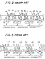
- FIG.2 shows the word line driver in a cross section taken along a line A-A in FIG.1
- FIG.3 shows the word line driver in a cross section taken along a line B-B in FIG.1.
- the word line driver shown in FIG.1 is provided with two boost signal lines 100 and 200 because this word line driver uses a word line activation signal which is predecoded with respect to the word decoder.
- the word line driver is made up of N-channel metal oxide semiconductor (MOS) transistors.
- Word lines 50, 52, 54, 56, 58 and 60 for outputting signals to a memory cell array extend parallel to each other.
- the boost signal lines 100 and 200 extend perpendicularly to these word lines 50 through 60.
- device isolation regions 7, 7′ and 7 ⁇ are formed in parallel to the word lines 50 through 60.
- the device isolation region 7 is formed between the word lines 54 and 56
- the device isolation region 7′ is formed between the word lines 50 and 52
- the device isolation region 7 ⁇ is formed between the word lines 58 and 60.
- Element regions 8, 8′, 9 and 9′ extend in parallel to the word lines 50 through 60.
- the device isolation 7′ isolates the element regions 8 an 9′
- the device isolation 7 isolates the element regions 8 and 9, and the device isolation 7 ⁇ isolates the element regions 8′ and 9.
- a driver 1 is formed within the element region 9′, drivers 2 and 3 are formed within the element region 8, drivers 4 and 5 are formed within the element region 9, and a driver 6 is formed within the element region 8′.
- Each of the drivers 1 through 6 are made up of MOS field effect transistors (MOSFETs) respectively having a gate electrode formed between a source region and a drain region.
- MOSFETs MOS field effect transistors
- the driver 2 includes a drain region 32 for inputting a word line activation signal from the boost signal line 100, a gate electrode 80, and a source region 20 which is coupled to the word line 50 via a word line contact 12.
- the driver 3 includes a drain region 32 for inputting a word line activation signal from the boost signal line 100, a gate electrode 82, and a source region 21 which is coupled to the word line 54 via a word line contact 10.
- the driver 6 includes a drain region 36 for inputting a word line activation signal from the boost signal line 100, a gate electrode 84, and a source region 22 which is coupled to the word line 58 via a word line contact 13.
- the drain region 32 which is connected to the boost signal line 100 is used in common by the drivers 2 and 3, as shown in FIGS.2 and 3.
- the driver 1 includes a drain region 38 for inputting a word line activation signal from the boost signal line 200, a gate electrode 86 and a source region 23 which is coupled to the word line 52 via a word line contact 14.
- the driver 4 includes a drain region 42 for inputting a word line activation signal from the boost signal line 200, a gate electrode 88, and a source region 24 which is coupled to the word line 56 via a word line contact 11.
- the driver 5 includes a drain region 42 for inputting a word line activation signal from the boost signal line 200, a gate electrode 90, and a source region 25 which is coupled to the word line 60 via a word line contact 15.
- the drain region 42 which is connected to the boost signal line 200 is used in common by the drivers 4 and 5, as shown in FIGS.2 and 3.
- the word lines 50 through 60 are respectively coupled to the memory cell array (not shown) which is provided above the boost signal line 100 in FIG.1.
- a decoder (not shown) is provided below the boost signal line 200 in FIG.1.
- the gate electrode 86 of the driver 1 and the gate electrode 80 of the driver 2 are connected in common to a signal line 70 from the decoder.
- the gate electrode 82 of the driver 3 and the gate electrode 88 of the driver 4 are connected in common to a signal line 72 from the decoder.
- the gate electrode 90 of the driver 5 and the gate electrode 84 of the driver 6 are connected in common to a signal line 74 from the decoder.
- the word line driver has the structure described above, it is possible to control two word lines using one decoder.
- a width occupied by the drivers used by one decoder will be referred to as "one decoder pitch”. Accordingly, it is possible to further reduce the size of the elements if this "one decoder pitch" can be reduced.
- Another and more specific object of the present invention is to provide a semiconductor memory device comprising a first word line, a second word line which extends in parallel to the first word line, word line activation signal line means which extends perpendicularly to the first and second word lines, a device isolation region which extends perpendicularly to the first and second word lines, a first driver for activating the first word line and comprising a first impurity region provided adjacent to the device isolation region and connected to the word line activation signal line means, a first gate electrode and a second impurity region connected to the first word line, a second driver for activating the second word line and comprising a third impurity region provided adjacent to the device isolation region on an opposite side from the first impurity region and connected to the word line activation signal line means, a second gate electrode and a fourth impurity region connected to the second word line, and a decoder connected to the first and second gate electrodes.
- the word line driver it is possible to provide the word line driver within a
- FIGS.4 through 8 a description will be given of a first embodiment of a semiconductor memory device according to the present invention, by referring to FIGS.4 through 8.
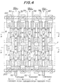
- FIG.4 shows a word line driver of the first embodiment of the semiconductor memory device according to the present invention in a plan view
- FIG.5 shows the word line driver in a cross section taken along a line A-A in FIG.4
- FIG.6 shows the word line driver in a cross section taken along a line B-B in FIG.4.
- FIGS.4 through 6 those parts which are the basically same as those corresponding parts in FIGS.1 through 3 are designated by the same reference numerals.
- the word line driver is provided with two boost signal lines 100 and 200 because the word line driver uses a word line activation signal which is predecoded with respect to a word decoder.
- Word lines 50, 52, 54, 56, 58 and 60 for outputting signals to a memory cell array extend parallel to each other.
- the boost signal lines 100 and 200 extend perpendicularly to these word lines 50 through 60.
- a device isolation region 7 is provided at an intermediate part between the two boost signal lines 100 and 200, and this device isolation region 7 extends perpendicularly to the word lines 50 through 60.
- An element region 8 is formed between the device isolation region 7 and the boost signal line 100, and an element region 9 is formed between the device isolation region 7 and the boost signal line 200.
- Drivers 2, 2′, 3, 3′, 6 and 6′ are formed within the element region 8.
- the driver 2 includes a drain region 30 for inputting a word activation signal from the boost signal line 100, a gate electrode 80 and a source region 20 which is coupled to the word line 50 via a word line contact 12.
- the driver 2′ includes a drain region 32 for inputting a word activation signal from the boost signal line 100, a gate electrode 81 and the source region 20 which is coupled to the word line 50 via the word line contact 12.
- the drivers 2 and 2′ form a transistor pair using the source region 20 in common.
- the driver 3 includes the drain region 32 for inputting a word activation signal from the boost signal line 100, a gate electrode 82 and a source region 21 which is coupled to the word line 54 via a word line contact 10.
- the driver 3' includes a drain region 34 for inputting a word activation signal from the boost signal line 100, a gate electrode 83 and the source region 21 which is coupled to the word line 54 via the word line contact 10.
- the drivers 3 and 3′ form a transistor pair using the source region 21 in common.
- the driver 6 includes a drain region 34 for inputting a word activation signal from the boost signal line 100, a gate electrode 84 and a source region 22 which is coupled to the word line 58 via a word line contact 13.
- the driver 6′ includes a drain region 36 for inputting a word activation signal from the boost signal line 100, a gate electrode 85 and the source region 22 which is coupled to the word line 58 via the word line contact 13.
- the drivers 6 and 6' form a transistor pair using the source region 22 in common.
- the drain region 32 which is connected to the boost signal line 100 is used in common by the drivers 2' and 3, and the drain region 34 is used in common by the drivers 3' and 6.
- Drivers 1, 1′, 4, 4′, 5 and 5′ are formed within the element region 9.
- the driver 1 includes a drain region 38 for inputting a word activation signal from the boost signal line 200, a gate electrode 86 and a source region 23 which is coupled to the word line 52 via a word line contact 14.
- the driver 1′ includes a drain region 40 for inputting a word activation signal from the boost signal line 200, a gate electrode 87 and the source region 23 which is coupled to the word line 52 via the word line contact 14.
- the drivers 1 and 1′ form a transistor pair using the source region 23 in common.
- the driver 4 includes the drain region 40 for inputting a word activation signal from the boost signal line 200, a gate electrode 88 and a source region 24 which is coupled to the word line 56 via a word line contact 11.
- the driver 4′ includes a drain region 42 for inputting a word activation signal from the boost signal line 200, a gate electrode 89 and the source region 24 which is coupled to the word line 56 via the word line contact 11.
- the drivers 4 and 4′ form a transistor pair using the source region 24 in common.
- the driver 5 includes a drain region 42 for inputting a word activation signal from the boost signal line 200, a gate electrode 90 and a source region 25 which is coupled to the word line 60 via a word line contact 15.
- the driver 5′ includes a drain region 44 for inputting a word activation signal from the boost signal line 200, a gate electrode 91 and the source region 25 which is coupled to the word line 60 via the word line contact 15.
- the drivers 5 and 5′ form a transistor pair using the source region 25 in common.
- the drain region 40 which is connected to the boost signal line 200 is used in common by the drivers 1′ and 4, and the drain region 42 is used in common by the drivers 4′ and 5.
- the word lines 50 through 60 connect to the memory cell array (not shown) which is provided above the boost signal line 100 in FIG.4.
- the decoder (not shown) is provided below the boost signal line 200 in FIG.4.
- the gate electrode 80 of the driver 2 and the gate electrode 86 of the driver 1 are connected.
- the gate electrode 81 of the driver 2′ and the gate electrode 87 of the driver 1′ are connected. Further, the two gate electrodes 86 and 87 are connected in common to a signal line 70 from the decoder.
- the gate electrode 82 of the driver 3 and the gate electrode 88 of the driver 4 are connected.
- the gate electrode 83 of the driver 3' and the gate electrode 89 of the driver 4′ are connected.
- the two gate electrodes 88 and 89 are connected in common to a signal line 72 from the decoder.
- the gate electrode 84 of the driver 6 and the gate electrode 90 of the driver 5 are connected.
- the gate electrode 85 of the driver 6′ and the gate electrode 91 of the driver 5′ are connected.
- the two gate electrodes 90 and 91 are connected in common to a signal line 74 from the decoder.
- This embodiment employs the so-called 1/2 predecoding in which two word lines are controlled by a single decoder.
- the "one decoder pitch" required to control a pair of word lines 54 and 56 is the length between the drain regions 32 and 34 or the drain regions 40 and 42.
- FIG.7 shows an equivalent circuit of an essential part of this embodiment.
- the driver circuit includes a decoder circuit and a word line driver using N-channel MOS transistors. Since this embodiment employs the 1/2 predecoding, the equivalent circuit shows the circuitry within "one decoder pitch" which is necessary to control a pair of word lines 54 and 56, for example.
- the word line 54 is connected to an N-channel transistor Q3 for inputting the word line activation signal from the boost signal line 100.
- the word line 56 is connected to an N-channel transistor Q4 for inputting the word line activation signal from the boost signal line 200.
- the N-channel transistor Q3 corresponds to the drivers 3 and 3′, and the N-channel transistor Q4 corresponds to the drivers 4 and 4′.
- the gate electrode of the N-channel transistor Q3 is connected to the gate electrode of the N-channel transistor Q4, and is coupled to an inverter 300 via a cut gate 310 within a decoder part which is surrounded by a dotted line.
- the gate electrode of an N-channel transistor 305 is connected to the gate electrode of an N-channel transistor 306, and is coupled to the inverter 300 via an inverter 301 within the decoder part.
- the inverter 300 is connected to an N-channel transistor 303 and a P-channel transistor 307.
- a signal A0 from a predecoder (not shown) is input to the gate electrode of the N-channel transistor 303.
- a signal A1 from the predecoder is input to the gate electrode of an N-channel transistor 304 which is connected in series to the N-channel transistor 303.
- a reset signal /R is input to the gate electrode of the P-channel transistor 307.
- the drain of a P-channel transistor 308 is connected to a node which connects the inverter 300 and the N-channel transistor 303.
- a node which connects the inverter 300 and the cut gate 310 is connected to the gate electrode of the P-channel transistor 308.
- Bits of a memory address for making access to a memory cell, other than the three least significant bits, are decoded in the predecoder (not shown) which is provided in a stage preceding the decoder part.
- the signals A0 and A1 which are input to the decoder part respectively correspond to the second and third least significant bits of the memory address.
- the word line activation signal from the boost signal lines 100 and 200 for driving the N-channel transistors Q3 and Q4 corresponds to the least significant bit of the memory address.
- the pair of word lines 54 and 56 is selected only when both the input signals A0 and A1 are high-level signals.
- the word line activation signal from the boost signal line 100 or 200 has a high level, the word line 54 or 56 is selected.
- the signal level at the gate electrodes of the N-channel transistors Q3 and Q4 become high and the signal level at the gate electrodes of the N-channel transistors 305 and 306 becomes low.
- the signal level of the word line activation signal from the boost signal line 100 becomes high
- the word line 54 is selected to the high level because the N-channel transistor Q3 is ON.
- the boost signal lines 100 and 200 correspond to the least significant bit of the memory address
- the signal level of the boost signal line 200 becomes low when the signal level at the boost signal line 100 is high, and although the N-channel transistor Q4 is ON, the signal level at the word line 56 is low.
- the signal level at the boost signal line 100 is low
- the word line activation signal from the boost signal line 200 has the high level, and the word line 56 is selected via the N-channel transistor Q4.
- the desired memory cell is selected in the above described manner.
- the driver circuit of this embodiment may also be formed using P-channel MOS transistors.
- FIG.8 shows an equivalent circuit of an essential part of this embodiment.
- the driver circuit includes a decoder circuit and a word line driver using P-channel MOS transistors. Particularly, the P-channel MOS transistors are used for the drivers 3, 3′, 4 and 4′.
- the driver circuit includes a decoder circuit and a word line driver using P-channel MOS transistors. Particularly, the P-channel MOS transistors are used for the drivers 3, 3′, 4 and 4′.
- FIG.8 those parts which are basically the same as those corresponding parts in FIG.7 are designated by the same reference numerals, and a description thereof will be omitted.
- the word line 54 is connected to a P-channel transistor Q3 for inputting the word line activation signal from the boost signal line 100.
- the word line 56 is connected to a P-channel transistor Q4 for inputting the word line activation signal from the boost signal line 200.
- the P-channel transistor Q3 corresponds to the drivers 3 and 3′, and the P-channel transistor Q4 corresponds to the drivers 4 and 4′.
- the gate electrodes of the P-channel transistors Q3 and Q4 and the gate electrodes of the N-channel transistors 305 and 306 are connected to a CMOS circuit of a level shift part which is surrounded by a dotted line.
- the CMOS circuit of the level shift part includes an N-channel transistor 401 and a P-channel transistor 403, and a voltage identical to the voltage of the word line activation signal from the P-channel transistors Q3 and Q4 is supplied to the gate electrodes.
- the P-channel transistor 403 and a P-channel transistor 402 are connected to a boost voltage source 400.
- the P-channel transistor 402 and the CMOS circuit are coupled to the inverter 300 of the decoder part via the cut gate 310.
- the inverter 300 is connected to the N-channel transistor 303 and the P-channel transistor 307.
- a signal A0 from a predecoder (not shown) is input to the gate electrode of the N-channel transistor 303.
- a signal A1 from the predecoder is input to the gate electrode of an N-channel transistor 304 which is connected in series to the N-channel transistor 303.
- a reset signal /R is input to the gate electrode of the P-channel transistor 307.
- the drain of the P-channel transistor 308 is connected to a node which connects the inverter 300 and the N-channel transistor 303.
- a node which connects the inverter 300 and the cut gate 310 is connected to the gate electrode of the P-channel transistor 308.
- this embodiment it is possible to eliminate the device isolation region which conventionally existed in parallel with the word lines within the "one decoder pitch".
- two word line contacts conventionally existed in a direction perpendicular to the word lines within the "one decoder pitch"
- only one word line contact is required within the "one decoder pitch” according to this embodiment. Accordingly, a sufficient margin is introduced in the width of the semiconductor memory device along the direction in which the "decoder pitch" is taken, and it becomes possible to ensure a sufficient gate length for the word line driver.
- the "decoder pitch" does not increase even when the width of the device isolation region increases.
- FIG.6 those parts which are the same as those corresponding parts in FIG.4 are designated by the same reference numerals, and a description thereof will be omitted.
- This embodiment is characterized by the modified shape of the gate electrodes of the drivers when compared to the first embodiment.
- ends of the gate electrodes of the driver pair are connected in an approximate U-shape.
- the gate electrodes 86 and 87 of the drivers 1 and 1′ are connected to surround the word line contact 14 of the source region 23.
- the gate electrodes 80 and 81 of the drivers 2 and 2′ are connected to surround the word line contact 12 of the source region 20.
- the gate electrodes 82 and 83 of the drivers 3 and 3′ are connected to surround the word line contact 10 of the source region 21.
- the gate electrodes 88 and 89 of the drivers 4 and 4' are connected to surround the word line contact 11 of the source region 24.
- the gate electrodes 90 and 91 of the drivers 5 and 5′ are connected to surround the word line contact 15 of the source region 25.
- the gate electrodes 84 and 85 of the drivers 6 and 6′ are connected to surround the word line contact 13 of the source region 22.
- FIG.10 shows a word line driver of the third embodiment in a plan view
- FIG.11 shows an equivalent circuit of an essential part of the third embodiment.
- FIG.10 those parts which are the same as those corresponding parts in FIG.4 are designated by the same reference numerals, and a description thereof will be omitted.
- FIG.11 those parts which are the same as those corresponding parts in FIGS.7 and 8 are designated by the same reference numerals, and a description thereof will be omitted.
- This embodiment is characterized in that no predecoding using the boost signal line is made and that a single decoder is provided with respect to one word line.
- the word line driver is formed from P-channel MOS transistors.
- the word lines 50, 52, 54, 46, 58 and 60 for outputting signals to a memory cell array are provided in parallel to each other.
- the memory cell array is provided above an external power source line 220 in FIG.10, and this external power source line 220 extends perpendicularly to the word lines 50 through 60.
- the element regions 8 and 9 extend perpendicularly to the word lines 50 through 60 on the opposite side from the memory cell array relative to the external power source line 220.
- the device isolation region 7 extends between the element regions 8 and 9.
- the drivers 2, 2′, 3, 3′, 6 and 6′ are formed within the element region 8.
- the driver 2 includes a source region 30′ which is connected to the external power source line 220, a gate electrode 80, and a drain region 20′ which is coupled to the word line 50 via a word line contact 12.
- the driver 2′ includes a source region 32′ which is connected to the external power source line 220, a gate electrode 81, and the drain region 20' which is coupled to the word line 50 via the word line contact 12.
- the drivers 2 and 2′ form a transistor pair using the drain region 20′ in common.
- the driver 3 includes a source region 32′ which is connected to the external power source line 220, a gate electrode 82, and a drain region 21′ which is coupled to the word line 54 via a word line contact 10.
- the driver 3′ includes a source region 34′ which is connected to the external power source line 220, a gate electrode 83, and the drain region 21′ which is coupled to the word line 54 via the word line contact 10.
- the drivers 3 and 3′ form a transistor pair using the drain region 21′ in common.
- the driver 6 includes a source region 34′ which is connected to the external power source line 220, a gate electrode 84, and a drain region 22′ which is coupled to the word line 58 via a word line contact 13.
- the driver 6′ includes a source region 36' which is connected to the external power source line 220, a gate electrode 85, and the drain region 22′ which is coupled to the word line 58 via the word line contact 13.
- the drivers 6 and 6′ form a transistor pair using the drain region 22′ in common.
- the source region 32′ which is connected to the external power source line 220 is used in common by the drivers 2′ and 3.
- the source region 34′ is used in common by the drivers 3′ and 6.
- the drivers 1, 1′, 4, 4′, 5 and 5′ are formed within the element region 9.
- the driver 1 includes a source region 38′ which is coupled to the external power source line 220 by a connection line 45 via the source region 30′, a gate electrode 86, and a drain region 23′ which is coupled to the word line 52 via a word line contact 14.
- the driver 1′ includes a source region 40′ which is coupled to the external power source line 220 by a connection line 46 via the source region 32′, a gate electrode 87, and the drain region 23′ which is coupled to the word line 52 via the word line contact 14.
- the drivers 1 and 1′ form a transistor pair using the drain region 23′ in common.
- the driver 4 includes a source region 40′ which is coupled to the external power source line 220 by the connection line 46 via the source region 32′, a gate electrode 88, and a drain region 24′ which is coupled to the word line 56 via a word line contact 11.
- the driver 4′ includes a source region 42′ which is coupled to the external power source line 220 by a connection line 47 via the source region 34′, a gate electrode 89, and the drain region 24′ which is coupled to the word line 56 via the word line contact 11.
- the drivers 4 and 4′ form a transistor pair using the drain region 24′ in common.
- the driver 5 includes a source region 42′ which is connected to the external power source line 220 by the connection line 47 via the source region 34′, a gate electrode 90, and a drain region 25′ which is coupled to the word line 60 via a word line contact 15.
- the driver 5′ includes a source region 44′ which is coupled to the external power source line 220 by a connection line 48 via the source region 36′, a gate electrode 91, and the drain region 25′ which is coupled to the word line 60 via the word line contact 15.
- the drivers 5 and 5′ form a transistor pair using the drain region 25′ in common.
- the source region 40′ which is coupled to the external power source line 220 via the connection line 46 is used in common by the drivers 1′ and 4.
- the source region 42′ is used in common by the drivers 4′ and 5.
- the word lines 50 through 60 are respectively connected to the memory cell array which is provided above the external power source line 220 in FIG.10.
- the gate electrode 80 of the driver 2 and the gate electrode 81 of the driver 2′ are integrally formed to surround the drain region 20′, and are coupled to a signal line 61 from the decoder by a signal contact 67.
- the gate electrodes 82 and 83 of the drivers 3 and 3′, the gate electrodes 84 and 85 of the drivers 6 and 6′, the gate electrodes 86 and 87 of the drivers 1 and 1′, the gate electrodes 88 and 89 of the drivers 4 and 4′, and the gate electrodes 90 and 91 of the drivers 5 and 5′ are formed similarly to the gate electrodes 80 and 81 of the drivers 2 and 2′, and are coupled to corresponding signal lines 63, 65, 62, 64 and 66 from the decoder via respective signal contacts 68, 69, ... .
- the word line driver does not make a predecoding. For this reason, the width corresponding to "one decoder pitch" of the first embodiment corresponds to the width of "two decoder pitches" of this third embodiment.
- the driver circuit includes a decoder circuit and a word line driver using P-channel MOS transistors. Since this embodiment does not make a predecoding, the equivalent circuit shows the circuitry within "one decoder pitch" which is necessary to control one word line by one decoder.
- the word line is connected to a P-channel transistor Q3 for inputting the word line activation signal (Vcc) from the external power source line 220.
- This P-channel transistor Q3 corresponds to each driver.
- the gate electrode of the P-channel transistor Q3 is connected to the gate electrode of an N-channel transistor 305, and is coupled to an N-channel transistor 303 and a P-channel transistor 307 via inverters 302 and 300 within a decoder part surrounded by a dotted line.
- a signal A0 from a predecoder (not shown) is input to the gate electrode of the N-channel transistor 303.
- a signal A1 from the predecoder is input to the gate electrode of an N-channel transistor 304 which is connected in series to the N-channel transistor 303.
- a reset signal /R is input to the gate electrode of the P-channel transistor 307.
- the drain of a P-channel transistor 308 is connected to a node which connects the inverter 300 and the N-channel transistor 303.
- a node which connects the inverters 300 and 302 is connected to the gate electrode of the P-channel transistor 308.
- Bits of a memory address for making access to a memory cell are decoded in the predecoder (not shown) which is provided in a stage preceding the decoder part.
- the signals A0 and A1 which are input to the decoder part respectively correspond to the first and second least significant bits of the memory address.
- the word line of the circuit shown in FIG.11 is selected only when the signal level of both the input signals A0 and A1 is high.
- the signal levels at the gate electrodes of the P-channel transistor Q3 and the N-channel transistor 305 become low.
- the signal level at the word line becomes high, and the desired memory cell is selected.
- the first and second embodiments described above employ the 1/2 predecoding. However, these embodiments may employ other predecodings such as a 1/4 predecoding in which four word lines are controlled by a single decoder.
Landscapes
- Engineering & Computer Science (AREA)
- Microelectronics & Electronic Packaging (AREA)
- Semiconductor Memories (AREA)
- Dram (AREA)
- Static Random-Access Memory (AREA)
Applications Claiming Priority (2)
| Application Number | Priority Date | Filing Date | Title |
|---|---|---|---|
| JP244585/90 | 1990-09-14 | ||
| JP2244585A JP2564695B2 (ja) | 1990-09-14 | 1990-09-14 | 半導体記憶装置 |
Publications (3)
| Publication Number | Publication Date |
|---|---|
| EP0475852A2 true EP0475852A2 (fr) | 1992-03-18 |
| EP0475852A3 EP0475852A3 (en) | 1995-10-11 |
| EP0475852B1 EP0475852B1 (fr) | 1998-01-14 |
Family
ID=17120911
Family Applications (1)
| Application Number | Title | Priority Date | Filing Date |
|---|---|---|---|
| EP91402446A Expired - Lifetime EP0475852B1 (fr) | 1990-09-14 | 1991-09-13 | Dispositif de mémoire à semi-conducteurs avec un circuit d'attaque de ligne de mot |
Country Status (5)
| Country | Link |
|---|---|
| US (1) | US5227996A (fr) |
| EP (1) | EP0475852B1 (fr) |
| JP (1) | JP2564695B2 (fr) |
| KR (1) | KR960001332B1 (fr) |
| DE (1) | DE69128676T2 (fr) |
Cited By (1)
| Publication number | Priority date | Publication date | Assignee | Title |
|---|---|---|---|---|
| DE19650715B4 (de) * | 1995-12-08 | 2007-06-06 | Hynix Semiconductor Inc., Ichon | Unterwortleitungstreiberschaltung und diese verwendende Halbleiterspeichervorrichtung |
Families Citing this family (6)
| Publication number | Priority date | Publication date | Assignee | Title |
|---|---|---|---|---|
| JPH07254275A (ja) * | 1994-01-31 | 1995-10-03 | Toshiba Corp | 半導体記憶装置 |
| US5636158A (en) * | 1995-03-13 | 1997-06-03 | Kabushiki Kaisha Toshiba | Irregular pitch layout for a semiconductor memory device |
| US6154056A (en) * | 1997-06-09 | 2000-11-28 | Micron Technology, Inc. | Tri-stating address input circuit |
| US6381166B1 (en) * | 1998-09-28 | 2002-04-30 | Texas Instruments Incorporated | Semiconductor memory device having variable pitch array |
| JP3566608B2 (ja) * | 1999-12-28 | 2004-09-15 | Necエレクトロニクス株式会社 | 半導体集積回路 |
| JP4632287B2 (ja) * | 2003-10-06 | 2011-02-16 | 株式会社日立製作所 | 半導体集積回路装置 |
Family Cites Families (7)
| Publication number | Priority date | Publication date | Assignee | Title |
|---|---|---|---|---|
| US4319342A (en) * | 1979-12-26 | 1982-03-09 | International Business Machines Corporation | One device field effect transistor (FET) AC stable random access memory (RAM) array |
| JPS6059677B2 (ja) * | 1981-08-19 | 1985-12-26 | 富士通株式会社 | 半導体記憶装置 |
| JPH073862B2 (ja) * | 1983-07-27 | 1995-01-18 | 株式会社日立製作所 | 半導体記憶装置 |
| JPS61110459A (ja) * | 1984-11-02 | 1986-05-28 | Nippon Telegr & Teleph Corp <Ntt> | 半導体メモリ |
| JPS61112365A (ja) * | 1984-11-07 | 1986-05-30 | Hitachi Ltd | 半導体集積回路装置 |
| JP2560020B2 (ja) * | 1987-02-18 | 1996-12-04 | 株式会社日立製作所 | 半導体記憶装置 |
| US4992981A (en) * | 1987-06-05 | 1991-02-12 | International Business Machines Corporation | Double-ended memory cell array using interleaved bit lines and method of fabrication therefore |
-
1990
- 1990-09-14 JP JP2244585A patent/JP2564695B2/ja not_active Expired - Lifetime
-
1991
- 1991-09-10 US US07/757,154 patent/US5227996A/en not_active Expired - Lifetime
- 1991-09-13 DE DE69128676T patent/DE69128676T2/de not_active Expired - Lifetime
- 1991-09-13 EP EP91402446A patent/EP0475852B1/fr not_active Expired - Lifetime
- 1991-09-14 KR KR1019910016041A patent/KR960001332B1/ko not_active Expired - Lifetime
Cited By (2)
| Publication number | Priority date | Publication date | Assignee | Title |
|---|---|---|---|---|
| DE19650715B4 (de) * | 1995-12-08 | 2007-06-06 | Hynix Semiconductor Inc., Ichon | Unterwortleitungstreiberschaltung und diese verwendende Halbleiterspeichervorrichtung |
| DE19655409B4 (de) * | 1995-12-08 | 2009-11-12 | Hynix Semiconductor Inc., Icheon | Halbleiterspeichervorrichtung |
Also Published As
| Publication number | Publication date |
|---|---|
| DE69128676T2 (de) | 1998-04-23 |
| KR960001332B1 (ko) | 1996-01-26 |
| US5227996A (en) | 1993-07-13 |
| JPH04123385A (ja) | 1992-04-23 |
| EP0475852A3 (en) | 1995-10-11 |
| EP0475852B1 (fr) | 1998-01-14 |
| JP2564695B2 (ja) | 1996-12-18 |
| DE69128676D1 (de) | 1998-02-19 |
Similar Documents
| Publication | Publication Date | Title |
|---|---|---|
| KR100246311B1 (ko) | 반도체 메모리소자 | |
| EP0712132B1 (fr) | Mémoire à semi-conducteurs | |
| US4951259A (en) | Semiconductor memory device with first and second word line drivers | |
| KR100200724B1 (ko) | 반도체 메모리장치의 서브 워드라인 드라이버 | |
| US5517038A (en) | Semiconductor device including three-dimensionally disposed logic elements for improving degree of integration | |
| EP0493640A1 (fr) | Cellule EEPROM avec une grille à un seul niveau de métal ayant une interface de lecture du circuit externe isolée de l'interface d'écriture effacement du circuit de programmation | |
| KR910000388B1 (ko) | 메모리셀 블록의 선택적 동작이 가능한 반도체 메모리장치 | |
| EP0475852B1 (fr) | Dispositif de mémoire à semi-conducteurs avec un circuit d'attaque de ligne de mot | |
| JP2994120B2 (ja) | 半導体記憶装置 | |
| EP0202910A2 (fr) | Circuit décodeur pour un dispositif de mémoire semi-conducteur | |
| KR960016426B1 (ko) | 반도체 집적회로 장치 | |
| US5896344A (en) | Local word line decoder for memory with 2 1/2 MOS devices | |
| EP0454998B1 (fr) | Dispositif de mémoire à semi-conducteurs | |
| US4555778A (en) | Semiconductor memory device | |
| US12315596B2 (en) | Word line driver, word line driver array, and semiconductor structure | |
| EP0201185B1 (fr) | Dispositif de mémoire à semi-conducteur | |
| EP0068861B1 (fr) | Circuit intégré décodeur | |
| US4924440A (en) | MOS gate array devices | |
| US5973345A (en) | Self-bootstrapping device | |
| JPH1117132A (ja) | 半導体記憶装置 | |
| JPS59152725A (ja) | マルチプレクサ | |
| KR0163540B1 (ko) | 고집적 반도체 메모리장치 | |
| JP3749294B2 (ja) | 半導体メモリ装置のデコーダ回路 | |
| JP3073511B2 (ja) | ダイナミック型半導体記憶装置 | |
| KR20020072769A (ko) | 프리챠지 회로 및 이를 이용한 반도체 장치 |
Legal Events
| Date | Code | Title | Description |
|---|---|---|---|
| PUAI | Public reference made under article 153(3) epc to a published international application that has entered the european phase |
Free format text: ORIGINAL CODE: 0009012 |
|
| AK | Designated contracting states |
Kind code of ref document: A2 Designated state(s): DE FR GB |
|
| PUAL | Search report despatched |
Free format text: ORIGINAL CODE: 0009013 |
|
| AK | Designated contracting states |
Kind code of ref document: A3 Designated state(s): DE FR GB |
|
| 17P | Request for examination filed |
Effective date: 19951120 |
|
| 17Q | First examination report despatched |
Effective date: 19960711 |
|
| GRAG | Despatch of communication of intention to grant |
Free format text: ORIGINAL CODE: EPIDOS AGRA |
|
| GRAG | Despatch of communication of intention to grant |
Free format text: ORIGINAL CODE: EPIDOS AGRA |
|
| GRAH | Despatch of communication of intention to grant a patent |
Free format text: ORIGINAL CODE: EPIDOS IGRA |
|
| GRAH | Despatch of communication of intention to grant a patent |
Free format text: ORIGINAL CODE: EPIDOS IGRA |
|
| GRAA | (expected) grant |
Free format text: ORIGINAL CODE: 0009210 |
|
| AK | Designated contracting states |
Kind code of ref document: B1 Designated state(s): DE GB |
|
| REF | Corresponds to: |
Ref document number: 69128676 Country of ref document: DE Date of ref document: 19980219 |
|
| EN | Fr: translation not filed | ||
| PLBE | No opposition filed within time limit |
Free format text: ORIGINAL CODE: 0009261 |
|
| STAA | Information on the status of an ep patent application or granted ep patent |
Free format text: STATUS: NO OPPOSITION FILED WITHIN TIME LIMIT |
|
| 26N | No opposition filed | ||
| REG | Reference to a national code |
Ref country code: GB Ref legal event code: IF02 |
|
| REG | Reference to a national code |
Ref country code: GB Ref legal event code: 732E |
|
| PGFP | Annual fee paid to national office [announced via postgrant information from national office to epo] |
Ref country code: GB Payment date: 20100908 Year of fee payment: 20 |
|
| PGFP | Annual fee paid to national office [announced via postgrant information from national office to epo] |
Ref country code: DE Payment date: 20100908 Year of fee payment: 20 |
|
| REG | Reference to a national code |
Ref country code: DE Ref legal event code: R071 Ref document number: 69128676 Country of ref document: DE |
|
| REG | Reference to a national code |
Ref country code: DE Ref legal event code: R071 Ref document number: 69128676 Country of ref document: DE |
|
| REG | Reference to a national code |
Ref country code: GB Ref legal event code: PE20 Expiry date: 20110912 |
|
| PG25 | Lapsed in a contracting state [announced via postgrant information from national office to epo] |
Ref country code: GB Free format text: LAPSE BECAUSE OF EXPIRATION OF PROTECTION Effective date: 20110912 |
|
| PG25 | Lapsed in a contracting state [announced via postgrant information from national office to epo] |
Ref country code: DE Free format text: LAPSE BECAUSE OF EXPIRATION OF PROTECTION Effective date: 20110914 |