EP0478014A2 - Steuerungssystem für einen Speicher - Google Patents
Steuerungssystem für einen Speicher Download PDFInfo
- Publication number
- EP0478014A2 EP0478014A2 EP91121095A EP91121095A EP0478014A2 EP 0478014 A2 EP0478014 A2 EP 0478014A2 EP 91121095 A EP91121095 A EP 91121095A EP 91121095 A EP91121095 A EP 91121095A EP 0478014 A2 EP0478014 A2 EP 0478014A2
- Authority
- EP
- European Patent Office
- Prior art keywords
- signal
- code
- sync signal
- sync
- block address
- Prior art date
- Legal status (The legal status is an assumption and is not a legal conclusion. Google has not performed a legal analysis and makes no representation as to the accuracy of the status listed.)
- Granted
Links
Images


Classifications
-
- G—PHYSICS
- G11—INFORMATION STORAGE
- G11B—INFORMATION STORAGE BASED ON RELATIVE MOVEMENT BETWEEN RECORD CARRIER AND TRANSDUCER
- G11B20/00—Signal processing not specific to the method of recording or reproducing; Circuits therefor
- G11B20/10—Digital recording or reproducing
-
- G—PHYSICS
- G11—INFORMATION STORAGE
- G11B—INFORMATION STORAGE BASED ON RELATIVE MOVEMENT BETWEEN RECORD CARRIER AND TRANSDUCER
- G11B27/00—Editing; Indexing; Addressing; Timing or synchronising; Monitoring; Measuring tape travel
- G11B27/10—Indexing; Addressing; Timing or synchronising; Measuring tape travel
- G11B27/19—Indexing; Addressing; Timing or synchronising; Measuring tape travel by using information detectable on the record carrier
- G11B27/28—Indexing; Addressing; Timing or synchronising; Measuring tape travel by using information detectable on the record carrier by using information signals recorded by the same method as the main recording
- G11B27/30—Indexing; Addressing; Timing or synchronising; Measuring tape travel by using information detectable on the record carrier by using information signals recorded by the same method as the main recording on the same track as the main recording
- G11B27/3027—Indexing; Addressing; Timing or synchronising; Measuring tape travel by using information detectable on the record carrier by using information signals recorded by the same method as the main recording on the same track as the main recording used signal is digitally coded
-
- G—PHYSICS
- G11—INFORMATION STORAGE
- G11B—INFORMATION STORAGE BASED ON RELATIVE MOVEMENT BETWEEN RECORD CARRIER AND TRANSDUCER
- G11B20/00—Signal processing not specific to the method of recording or reproducing; Circuits therefor
- G11B20/10—Digital recording or reproducing
- G11B20/10527—Audio or video recording; Data buffering arrangements
-
- G—PHYSICS
- G11—INFORMATION STORAGE
- G11B—INFORMATION STORAGE BASED ON RELATIVE MOVEMENT BETWEEN RECORD CARRIER AND TRANSDUCER
- G11B20/00—Signal processing not specific to the method of recording or reproducing; Circuits therefor
- G11B20/10—Digital recording or reproducing
- G11B20/12—Formatting, e.g. arrangement of data block or words on the record carriers
- G11B20/1201—Formatting, e.g. arrangement of data block or words on the record carriers on tapes
- G11B20/1207—Formatting, e.g. arrangement of data block or words on the record carriers on tapes with transverse tracks only
- G11B20/1208—Formatting, e.g. arrangement of data block or words on the record carriers on tapes with transverse tracks only for continuous data, e.g. digitised analog information signals, pulse code modulated [PCM] data
-
- G—PHYSICS
- G11—INFORMATION STORAGE
- G11B—INFORMATION STORAGE BASED ON RELATIVE MOVEMENT BETWEEN RECORD CARRIER AND TRANSDUCER
- G11B20/00—Signal processing not specific to the method of recording or reproducing; Circuits therefor
- G11B20/10—Digital recording or reproducing
- G11B20/18—Error detection or correction; Testing, e.g. of drop-outs
- G11B20/1806—Pulse code modulation systems for audio signals
- G11B20/1809—Pulse code modulation systems for audio signals by interleaving
-
- G—PHYSICS
- G11—INFORMATION STORAGE
- G11B—INFORMATION STORAGE BASED ON RELATIVE MOVEMENT BETWEEN RECORD CARRIER AND TRANSDUCER
- G11B20/00—Signal processing not specific to the method of recording or reproducing; Circuits therefor
- G11B20/10—Digital recording or reproducing
- G11B20/18—Error detection or correction; Testing, e.g. of drop-outs
- G11B20/1833—Error detection or correction; Testing, e.g. of drop-outs by adding special lists or symbols to the coded information
-
- H—ELECTRICITY
- H04—ELECTRIC COMMUNICATION TECHNIQUE
- H04N—PICTORIAL COMMUNICATION, e.g. TELEVISION
- H04N5/00—Details of television systems
- H04N5/76—Television signal recording
- H04N5/91—Television signal processing therefor
- H04N5/93—Regeneration of the television signal or of selected parts thereof
- H04N5/935—Regeneration of digital synchronisation signals
-
- H—ELECTRICITY
- H04—ELECTRIC COMMUNICATION TECHNIQUE
- H04N—PICTORIAL COMMUNICATION, e.g. TELEVISION
- H04N9/00—Details of colour television systems
- H04N9/79—Processing of colour television signals in connection with recording
- H04N9/80—Transformation of the television signal for recording, e.g. modulation, frequency changing; Inverse transformation for playback
- H04N9/802—Transformation of the television signal for recording, e.g. modulation, frequency changing; Inverse transformation for playback involving processing of the sound signal
-
- G—PHYSICS
- G11—INFORMATION STORAGE
- G11B—INFORMATION STORAGE BASED ON RELATIVE MOVEMENT BETWEEN RECORD CARRIER AND TRANSDUCER
- G11B20/00—Signal processing not specific to the method of recording or reproducing; Circuits therefor
- G11B20/10—Digital recording or reproducing
- G11B20/12—Formatting, e.g. arrangement of data block or words on the record carriers
- G11B20/1201—Formatting, e.g. arrangement of data block or words on the record carriers on tapes
- G11B20/1211—Formatting, e.g. arrangement of data block or words on the record carriers on tapes with different data track configurations
-
- G—PHYSICS
- G11—INFORMATION STORAGE
- G11B—INFORMATION STORAGE BASED ON RELATIVE MOVEMENT BETWEEN RECORD CARRIER AND TRANSDUCER
- G11B2220/00—Record carriers by type
- G11B2220/90—Tape-like record carriers
-
- G—PHYSICS
- G11—INFORMATION STORAGE
- G11B—INFORMATION STORAGE BASED ON RELATIVE MOVEMENT BETWEEN RECORD CARRIER AND TRANSDUCER
- G11B2220/00—Record carriers by type
- G11B2220/90—Tape-like record carriers
- G11B2220/91—Helical scan format, wherein tracks are slightly tilted with respect to tape direction, e.g. VHS, DAT, DVC, AIT or exabyte
- G11B2220/913—Digital audio tape [DAT] format
Definitions
- This invention relates to a memory control system used for recording and reproducing serial digital data.
- a digital audio tape recorder DAT
- a recording signal is formatted in a constant block period Bt as shown in Fig. 4, in which serial digital data D0, D1, ..., D n are preceded by a synchronizing signal (SYNC) with a specific code pattern, a record identification code (ID), a block address code (BA), and an error detection code (EDC) for the ID and BA.
- SYNC synchronizing signal
- ID record identification code
- BA block address code
- EDC error detection code
- the data of the identification code (ID) indicative of the content of recorded data, etc. is denoted by the symbol W1
- the data of the address code BA is denoted by the symbol W2
- the data of the error detection code EDC is denoted by the symbol P.
- the reproducing section has a sync generator providing the same code pattern as that of the recording section, and it compares the reproduced serial digital data with the sync pattern sequentially so as to decide a reproduced signal, when it coincides with the sync pattern, to be a sync signal so that it is used as a reference signal for the successive signal processing. This is the prevalent technique of serial digital data recording and reproduction.
- the R-DAT employs a modulation system called "8-10 modulation" with its sync signal (SYNC) having a special pattern which does not appear in data normally, so that the accuracy of sync signal detection is appreciably high.
- SYNC sync signal
- a modulation system having a special sync pattern cannot be used by some reason, for example, because of the band limitation of the recording signals such as when recording both an analog video signal and a digital audio signal, it becomes inevitable to use a code pattern contained in data as a sync singal. In this case, false sync signals other than the valid sync signal will appear with high probability, and normal signal processing will be difficult.
- this problem may be solved by increasing the word length of the sync signal (SYNC), it will result disadvantageously in an increased recording frequency or a degraded signal transmission rate.
- a conventional breakthrough technique for ensuring the sync signal detection without an increased word length of the sync signal is, in addition to the use of a first sync signal detection circuit, to detect predetermined regularity in the contents of two consecutive block address codes BA to utilize it as a second sync signal so that a final sync signal is obtained from a logical product of both the first and second sync signals, as disclosed, for example, in Japanese Patent Unexamined Publication No. 60-137150.
- the block address code BA generally uses a series of binary numbers increasing continuously from zero, and the detection of a predetermined difference in the value between two consecutive address codes ensures the sync signal detection.
- Fig. 5 is a block diagram showing a conventional memory control apparatus.
- serial digital data is inputted through an input terminal 2, and a sync signal detecting circuit 3 detects the sync signal and produces signals which are in phase with the sync signal.
- the serial digital data is also applied to a block address latch circuit 4, in which the address code BA is latched in response to a latch pulse supplied from the sync signal detecting circuit 3.
- the serial digital data is further fed to a parity check circuit 5, in which a positive parity check or a negative parity check is made in accordance with the following equation for the code structure shown in Fig. 4, for example.
- the sync signal detecting circuit 3 applies one output thereof to a clock terminal of a block address counter circuit 6, which further receives at its reset terminal rotary head switching pulses (the signal S1 shown in Fig. 2) indicative of the rotational position of the rotary head (not shown) which are supplied through an input terminal 1.
- the block address counter circuit 6 has its contents cleared at the edge of a head switching pulse and counts the sync signal until it is cleared by a next head switching pulse. This operation is repeated.
- numerals indicative of respective short slanting lines crossing the connection lines show bit numbers of digital signals sent through the connection lines, respectively.
- the block address counter circuit 6 and the block address latch circuit 4 apply their outputs (8 bits) to a block address anticoincidence circuit 8, which decides whether both block address values coincide with each other.
- the outputs of the block address anticoincidence circuit 8 and the parity check circuit 5 are applied to an AND gate 7, which outputs a pulse when the parity check result is correct and at the same time the block address values do not coincide with each other, and the output pulse is applied to the load terminal L of the block address counter circuit 6, and the 8-bit output of the block address latch circuit 4 is applied to the data terminal D of the block address counter circuit 6 so that the address value of the block address latch circuit 4 is loaded in the block address counter circuit 6.
- the block address counter circuit 6 produces an 8-bit output, which is outputted through an output terminal 9, and it forms a part of an address signal value for storing the reproduced digital data in a RAM (Random Access Memory).
- the sync signal detecting circuit 3 and the block address counter circuit 6 supply their outputs to a write signal generating circuit 10, which provides an output through an output terminal 11, and it is used as a write signal for storing the reproduced digital data in the RAM.
- an analog audio signal is digitized at a sampling frequency f s of 48 kHz, for example, so that a frequency ratio of the sampling frequency f s of 48 KHz to the field frequency f v of the video signal of 59.94 Hz in the NTSC system becomes 800.8.
- the number of data in one field is divided into two kinds, that is, a greater number and a smaller number (e.g., 792 and 810), and supplementary dummy data is added to the field containing a small number of data (792 data in one field) to effect recording.
- the MSB of the address code BA in Fig. 4 is used to record the information indicative of the presence or absence of the supplementary dummy data
- the block address value is recorded in 7 bits.
- the block address code W2 include the o-address (0000000) to 127-address (1111111).
- the next 128-address is indicated by (0000000)
- the block addresses are recorded in a magnetic tape with these bit indications.
- the 8-bit block address value for the reproduction cannot be produced directly from the recording block address value, since the recording block address is recorded in 7 bits on the magnetic tape.
- An object of this invention is to provide, in the case of recording and reproducing a digitized audio signal along with a video signal, a memory control system comprising a sync signal detecting circuit, a block address generating circuit and a write signal generating circuit for storing the digital data in the RAM.
- the memory control system of this invention utilizes a first sync signal, which is detected by making a comparison of coincidence of a reproduced sync signal with a sync signal pattern, and an error detection signal, which is produced by conducting a predetermined computation on an auxiliary code, an address code and an error detection code which are added along with a sync signal, so that the first sync signal is passed to be used as a second sync signal only when the error detection signal indicates the absence of error.
- the error detection code, etc. are utilized as a kind of a sync signal in addition to a first sync signal detected by making a comparison of coincidence of the reproduced sync signal with the sync pattern, and a logical-OR operation on both signals are conducted to elevate the precision of the sync signal detection.
- a result of the error detection of the additional codes when a sync signal is dropped, has low validity, and when a word length of the whole error detection code system is relatively short, the influence of a code error is small and it can be of sufficient use as a reference signal for distinguishing pseudo or false sync signals.
- an equivalent advantage of a substantially increased word length of a sync signal can be obtained, so that the sync signal detection with high precision, which is completed in a block, is accomplished without using the regularity between a plurality of blocks.
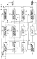
- Fig. 1 is a block diagram showing the memory control system embodying the present invention
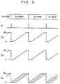
- Fig. 2 is a waveform diagram showing the signals appearing at various portions in Fig. 1.
- an input terminal 2 in Fig. 1 receives serial digital data
- a sync signal detecting circuit 3 detects the sync signal and produces a signal which are in phase with the sync signal.
- a block address latch circuit 4 extracts and latches an address code BA in the serial digital data in response to the latch pulse supplied from the sync signal detecting circuit 3.
- a parity check circuit 5 implements an even-parity test or an odd-parity test for the serial digital data in accordance with the following equation for the code structure shown in Fig. 4, for example, in response to a pulse supplied from the sync signal detecting circuit 3.
- p W1 ⁇ W2 or W1 ⁇ ⁇ ⁇ W2 ⁇ where symbol ⁇ denotes an exclusive-OR operation.
- the output of the sync signal detecting circuit 3 is applied to a clock input terminal of a block address counter circuit 6, and a head switching pulse signal (shown by S1 in Fig. 2) indicative of a rotational position of the rotary head (not shown) is supplied through an input terminal 1 and is applied to a reset terminal of the block address counter circuit 6.
- the count value of the block address counter circuit 6 is shown by signal S2 in Fig. 2.
- the block address counter circuit 6 is reset by the head switching pulse, and then it restarts to count up the sync signal using it as a clock signal until it reaches the maximum block address value (134) and stops there. Then, the counter is reset by a next head switching pulse signal, and these operations are repeated.
- the block address counter circuit 6 and the block address latch circuit 4 apply their lower-order 7-bit outputs to a block address anticoincidence circuit 8, which tests whether both block address values are equal to each other.
- the lower-order 7-bit output from the block address latch circuit 4 and the most significant 1-bit output from the block address counter 6 are applied to a composed block address generating circuit 21, which produces a composed block address value, with the most significant bit being supplied from the output of the block address counter circuit 6 and with the lower-order 7 bits being supplied from the output of the block address latch circuit 4.
- a reference block address generating circuit or a predicted address generating circuit 22, which is formed of a counter circuit, receives at its reset terminal a head switching pulse signal supplied from the input terminal 1, and it operates to count up an internal reference clock.
- the content of the counter is shown analogously by signal S3 in Fig. 2.
- the circuit 22 is reset by the head switching pulse signal, and then it restarts to count up the internal reference clock until it reaches the maximum block address value (134) and stops there. These operations are repeated, and block address values corresponding to the head position are generated.
- the reference block address generating circuit 22 and the composed block address generating circuit 21 apply their 8-bit outputs to a first address value comparing circuit 23.
- the circuit 23 further compares the computation result N1 with a predetermined value
- the parity check circuit 5, the block address anticoincidence circuit 8 and the first address value comparing circuit 23 apply their outputs to an AND gate circuit 7, which produces an output pulse on condition that the parity test result is correct, the block address values do not coincide with each other, and besides the following condition is met.
- the signal S4 in Fig. 2 shows a range which satisfies this condition.
- the broken line shows the signal S3, and the parallelogram shown by the solid line and including the broken line as its center line represents the above-mentioned range.
- the output pulse of the AND gate circuit 7 is applied to a load terminal L of the block address counter circuit 6.
- the composed block address generating circuit 21 has its 8-bit output applied to a data input terminal D and loaded in the block address counter circuit 6 in response to the load pulse supplied from the AND gate circuit 7.
- the 8-bit output of the block address counter circuit 6 is sent out through an output terminal 9 to form a part of an address value for storing the reproduced digital data in the RAM.
- the sync signal detecting circuit 3 and the block address counter circuit 6 apply their outputs to a write signal generating circuit 10, and the block address counter circuit 6 and the reference block address generating circuit 22 apply their 8-bit outputs to a second address value comparing circuit 24.
- the second address value comparing circuit 24 compares the computation result N2 with a predetermined value
- the write signal generating circuit 10 and the second address value comparing circuit 24 apply their outputs to an AND gate circuit 25, which produces a write signal when the following condition is met.
- This condition is represented by the internal area of the parallelogram of the signal S4 shown in Fig. 2 by the solid line and including the broken line as its center line.
- the write signal is sent out through an output terminal 11, and it is used as a write signal for storing the reproduced digital data in the RAM.
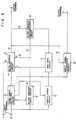
- Fig. 3 shows a specific circuit arrangement of the sync signal detecting circuit 3 in Fig. 1.
- 51 is an input terminal for receiving serial digital data at the time of reproduction
- 52a-52d are shift registers for effecting serial-to-parallel conversion
- 53 is a sync pattern generator which is arranged beforehand in the reproducing section and which is identical with that in the recording section
- 54 is a sync pattern comparator which makes a comparison of coincidence of the parallel digital data produced by the shift register 52a with pattern data generated by the sync pattern generator 53 and produces a first sync signal a upon detection of coincidence
- 55 is a parity generator for generating an error detection code by performing a predetermined computation on the parallel digital data produced by the shift registers 52b and 52c
- 56 is a parity checker, which makes a comparison of coincidence of the parity code produced in the reproducing section with the parity code added at the time of recording, and produces an error signal b upon detection of anticoincidence
- 57 is an AND gate circuit which produces
- this embodiment of the present invention utilizes the regularity of the successive timing relation of the sync signal and the error detection signal within the same block.
- each code other than the sync signal has 8 bits.
- the 8-bit error detection code has error detection probability of 2 ⁇ 8, which is mathematically proved to be equivalent in the capability to the 8-bit sync signal pattern. In addition to the original 8-bit sync signal pattern, 16-bit sync detection accuracy in total is attained by using the 8-bit sync signal pattern.
- the odd parity test is effective for ensuring the error detection.
- the address code and the error detection code to be equivalently an 8-bit sync signal to be added to the proper 8-bit sync signal, it becomes possible to realize the sync signal detection which is completed in one block and has substantial capability of 16-bit sync signal detection without increasing a length of the sync signal.
- the error detection code, etc. have a 8-bit code length
- any optional value may be used to meet the requirement of the system specifications.
Landscapes
- Engineering & Computer Science (AREA)
- Signal Processing (AREA)
- Multimedia (AREA)
- Signal Processing For Digital Recording And Reproducing (AREA)
Applications Claiming Priority (7)
| Application Number | Priority Date | Filing Date | Title |
|---|---|---|---|
| JP147586/87 | 1987-06-12 | ||
| JP62147586A JP2663441B2 (ja) | 1987-06-12 | 1987-06-12 | 同期信号検出方法 |
| JP62215806A JPH0727684B2 (ja) | 1987-08-28 | 1987-08-28 | ブロックアドレス発生装置 |
| JP215806/87 | 1987-08-28 | ||
| JP62252127A JPH0194566A (ja) | 1987-10-06 | 1987-10-06 | ブロックアドレス発生装置 |
| JP252127/87 | 1987-10-06 | ||
| EP88109301A EP0294841B1 (de) | 1987-06-12 | 1988-06-10 | Steuerungssystem für einen Speicher |
Related Parent Applications (1)
| Application Number | Title | Priority Date | Filing Date |
|---|---|---|---|
| EP88109301.7 Division | 1988-06-10 |
Publications (3)
| Publication Number | Publication Date |
|---|---|
| EP0478014A2 true EP0478014A2 (de) | 1992-04-01 |
| EP0478014A3 EP0478014A3 (en) | 1992-04-29 |
| EP0478014B1 EP0478014B1 (de) | 1995-03-15 |
Family
ID=27319387
Family Applications (2)
| Application Number | Title | Priority Date | Filing Date |
|---|---|---|---|
| EP91121095A Expired - Lifetime EP0478014B1 (de) | 1987-06-12 | 1988-06-10 | Steuerungssystem für einen Speicher |
| EP88109301A Expired - Lifetime EP0294841B1 (de) | 1987-06-12 | 1988-06-10 | Steuerungssystem für einen Speicher |
Family Applications After (1)
| Application Number | Title | Priority Date | Filing Date |
|---|---|---|---|
| EP88109301A Expired - Lifetime EP0294841B1 (de) | 1987-06-12 | 1988-06-10 | Steuerungssystem für einen Speicher |
Country Status (4)
| Country | Link |
|---|---|
| US (1) | US5021897A (de) |
| EP (2) | EP0478014B1 (de) |
| KR (1) | KR910008396B1 (de) |
| DE (2) | DE3884467T2 (de) |
Cited By (2)
| Publication number | Priority date | Publication date | Assignee | Title |
|---|---|---|---|---|
| EP0735535A3 (de) * | 1995-03-31 | 1997-08-13 | Samsung Electronics Co Ltd | Adaptives Verfahren zum Schutz von Synchronisationsblöcken in digitalen Wiedergabesystemen und Gerät dafür |
| CN1073737C (zh) * | 1995-09-06 | 2001-10-24 | 三星电子株式会社 | 同步检测与保护电路以及其方法 |
Families Citing this family (8)
| Publication number | Priority date | Publication date | Assignee | Title |
|---|---|---|---|---|
| JP2840680B2 (ja) * | 1989-07-28 | 1998-12-24 | ソニー株式会社 | 再生装置 |
| US5276561A (en) * | 1989-07-28 | 1994-01-04 | Sony Corporation | Apparatus for reproducing digital signal |
| US5644446A (en) * | 1992-07-06 | 1997-07-01 | Industrial Technology Research Institute | Rotary-head digital reproducing/recording method and apparatus with block address-based area signal generation |
| US5790264A (en) * | 1995-06-23 | 1998-08-04 | Olympus Optical Co., Ltd. | Information reproduction apparatus |
| JPH10340546A (ja) * | 1997-06-05 | 1998-12-22 | Canon Inc | 再生装置及び再生方法 |
| GB2422477A (en) * | 2005-01-21 | 2006-07-26 | Hewlett Packard Development Co | Tape drive apparatus for identifying data fragments |
| US8098657B2 (en) * | 2005-05-31 | 2012-01-17 | Broadcom Corporation | System and method for providing data commonality in a programmable transport demultiplexer engine |
| US7697537B2 (en) * | 2006-03-21 | 2010-04-13 | Broadcom Corporation | System and method for using generic comparators with firmware interface to assist video/audio decoders in achieving frame sync |
Family Cites Families (10)
| Publication number | Priority date | Publication date | Assignee | Title |
|---|---|---|---|---|
| DE3151251A1 (de) * | 1981-12-24 | 1983-07-07 | Robert Bosch Gmbh, 7000 Stuttgart | Verfahren und schaltungsanordnung zur wiedergabe digital codierter signale |
| GB2120423B (en) * | 1982-04-26 | 1985-10-09 | Sony Corp | Sequential data block address processing circuits |
| US4692816A (en) * | 1983-07-08 | 1987-09-08 | Victor Company Of Japan Ltd. | Digital data transmitting system for transmitting digital data a number of times depending on an information content of the digital data |
| JPS60137150A (ja) * | 1983-12-26 | 1985-07-20 | Sony Corp | 同期信号抽出回路 |
| US4622600A (en) * | 1983-12-26 | 1986-11-11 | Hitachi, Ltd. | Rotary-head type PCM data recording/reproducing method and apparatus with a redundancy-reduced control data format |
| GB2159020B (en) * | 1984-05-16 | 1987-11-18 | Sony Corp | Methods of and apparatus for use in decoding digital data |
| JPH0673225B2 (ja) * | 1984-11-06 | 1994-09-14 | 株式会社日立製作所 | デイジタル情報再生装置における時間軸補正装置 |
| JPH0668883B2 (ja) * | 1985-06-19 | 1994-08-31 | ソニー株式会社 | デジタル同期パタ−ン抽出方法 |
| KR900008446B1 (ko) * | 1985-11-13 | 1990-11-22 | 가부시끼가이샤 히다찌세이사꾸쇼 | 음성신호를위한표본화주파수와회전헤드스캔너의회전주파수사이에서비동기관계를갖는음성신호의pcm기록재생장치 |
| JPS62223857A (ja) * | 1986-03-25 | 1987-10-01 | Victor Co Of Japan Ltd | 同期信号抜き出し回路 |
-
1988
- 1988-06-07 US US07/203,107 patent/US5021897A/en not_active Expired - Fee Related
- 1988-06-10 DE DE88109301T patent/DE3884467T2/de not_active Expired - Fee Related
- 1988-06-10 EP EP91121095A patent/EP0478014B1/de not_active Expired - Lifetime
- 1988-06-10 DE DE3853369T patent/DE3853369T2/de not_active Expired - Fee Related
- 1988-06-10 EP EP88109301A patent/EP0294841B1/de not_active Expired - Lifetime
- 1988-06-11 KR KR1019880007033A patent/KR910008396B1/ko not_active Expired
Cited By (3)
| Publication number | Priority date | Publication date | Assignee | Title |
|---|---|---|---|---|
| EP0735535A3 (de) * | 1995-03-31 | 1997-08-13 | Samsung Electronics Co Ltd | Adaptives Verfahren zum Schutz von Synchronisationsblöcken in digitalen Wiedergabesystemen und Gerät dafür |
| US5848218A (en) * | 1995-03-31 | 1998-12-08 | Samsung Electronics Co., Ltd. | Adaptive sync protection method in digital reproduction systems and apparatus therefor |
| CN1073737C (zh) * | 1995-09-06 | 2001-10-24 | 三星电子株式会社 | 同步检测与保护电路以及其方法 |
Also Published As
| Publication number | Publication date |
|---|---|
| EP0478014A3 (en) | 1992-04-29 |
| KR890001066A (ko) | 1989-03-18 |
| EP0294841A2 (de) | 1988-12-14 |
| US5021897A (en) | 1991-06-04 |
| KR910008396B1 (ko) | 1991-10-15 |
| DE3853369T2 (de) | 1995-11-23 |
| DE3853369D1 (de) | 1995-04-20 |
| DE3884467D1 (de) | 1993-11-04 |
| EP0294841B1 (de) | 1993-09-29 |
| DE3884467T2 (de) | 1994-05-11 |
| EP0478014B1 (de) | 1995-03-15 |
| EP0294841A3 (en) | 1990-01-17 |
Similar Documents
| Publication | Publication Date | Title |
|---|---|---|
| EP0415853B1 (de) | Digitales Datenübertragungssystem mit Fehlererkennung und Fehlerkorrektur | |
| US4716567A (en) | Method of transmitting digital data in which error detection codes are dispersed using alternate delay times | |
| US4775901A (en) | Apparatus and method for preventing unauthorized dubbing of a recorded signal | |
| EP0367217B1 (de) | Verfahren zur Aufzeichnung und Wiedergabe von Informationssignalen und Gerät dafür | |
| US4145683A (en) | Single track audio-digital recorder and circuit for use therein having error correction | |
| EP0232133B1 (de) | Digitale Signalfehlerkorrektur | |
| US4704640A (en) | Method and apparatus for recording PCM signal | |
| EP0478014B1 (de) | Steuerungssystem für einen Speicher | |
| US4292684A (en) | Format for digital tape recorder | |
| US5228041A (en) | Sync signal detection system in a memory system for recording and reproducing block unit data | |
| US3883891A (en) | Redundant signal processing error reduction technique | |
| US4314355A (en) | Apparatus and method for receiving digital data at a first rate and outputting the data at a different rate | |
| EP0418885B1 (de) | Gerät zur Übertragung von digitalen Daten | |
| US4173014A (en) | Apparatus and method for receiving digital data at a first rate and outputting the data at a different rate | |
| US4872171A (en) | Method for recording digital data so as to avoid operational error on reproduction | |
| US4796243A (en) | Time base correcting apparatus | |
| US5276561A (en) | Apparatus for reproducing digital signal | |
| JPH0347613B2 (de) | ||
| US4870647A (en) | Digital signal demodulator | |
| JP2663441B2 (ja) | 同期信号検出方法 | |
| JP3282425B2 (ja) | ディジタル信号記録装置 | |
| KR100223160B1 (ko) | 디지탈-브이씨알(d-vcr)의 동기신호 기록.검출방법 및 그 장치 | |
| JPH05128742A (ja) | デジタル同期検出装置 | |
| KR0162222B1 (ko) | 의사동기신호 제거장치 | |
| JP2000285604A (ja) | 再生装置及び再生方法 |
Legal Events
| Date | Code | Title | Description |
|---|---|---|---|
| PUAI | Public reference made under article 153(3) epc to a published international application that has entered the european phase |
Free format text: ORIGINAL CODE: 0009012 |
|
| PUAL | Search report despatched |
Free format text: ORIGINAL CODE: 0009013 |
|
| AC | Divisional application: reference to earlier application |
Ref document number: 294841 Country of ref document: EP |
|
| AK | Designated contracting states |
Kind code of ref document: A2 Designated state(s): DE FR GB NL |
|
| AK | Designated contracting states |
Kind code of ref document: A3 Designated state(s): DE FR GB NL |
|
| 17P | Request for examination filed |
Effective date: 19920423 |
|
| 17Q | First examination report despatched |
Effective date: 19940704 |
|
| GRAA | (expected) grant |
Free format text: ORIGINAL CODE: 0009210 |
|
| AC | Divisional application: reference to earlier application |
Ref document number: 294841 Country of ref document: EP |
|
| AK | Designated contracting states |
Kind code of ref document: B1 Designated state(s): DE FR GB NL |
|
| REF | Corresponds to: |
Ref document number: 3853369 Country of ref document: DE Date of ref document: 19950420 |
|
| PGFP | Annual fee paid to national office [announced via postgrant information from national office to epo] |
Ref country code: GB Payment date: 19950530 Year of fee payment: 8 |
|
| PGFP | Annual fee paid to national office [announced via postgrant information from national office to epo] |
Ref country code: NL Payment date: 19950627 Year of fee payment: 8 |
|
| PGFP | Annual fee paid to national office [announced via postgrant information from national office to epo] |
Ref country code: FR Payment date: 19950630 Year of fee payment: 8 |
|
| ET | Fr: translation filed | ||
| PGFP | Annual fee paid to national office [announced via postgrant information from national office to epo] |
Ref country code: DE Payment date: 19950831 Year of fee payment: 8 |
|
| PLBE | No opposition filed within time limit |
Free format text: ORIGINAL CODE: 0009261 |
|
| STAA | Information on the status of an ep patent application or granted ep patent |
Free format text: STATUS: NO OPPOSITION FILED WITHIN TIME LIMIT |
|
| 26N | No opposition filed | ||
| PG25 | Lapsed in a contracting state [announced via postgrant information from national office to epo] |
Ref country code: GB Effective date: 19960610 |
|
| PG25 | Lapsed in a contracting state [announced via postgrant information from national office to epo] |
Ref country code: NL Effective date: 19970101 |
|
| GBPC | Gb: european patent ceased through non-payment of renewal fee |
Effective date: 19960610 |
|
| PG25 | Lapsed in a contracting state [announced via postgrant information from national office to epo] |
Ref country code: FR Effective date: 19970228 |
|
| PG25 | Lapsed in a contracting state [announced via postgrant information from national office to epo] |
Ref country code: DE Effective date: 19970301 |
|
| NLV4 | Nl: lapsed or anulled due to non-payment of the annual fee |
Effective date: 19970101 |
|
| REG | Reference to a national code |
Ref country code: FR Ref legal event code: ST |