EP0480136B1 - Atomkraft-Mikroskopie - Google Patents
Atomkraft-Mikroskopie Download PDFInfo
- Publication number
- EP0480136B1 EP0480136B1 EP91112362A EP91112362A EP0480136B1 EP 0480136 B1 EP0480136 B1 EP 0480136B1 EP 91112362 A EP91112362 A EP 91112362A EP 91112362 A EP91112362 A EP 91112362A EP 0480136 B1 EP0480136 B1 EP 0480136B1
- Authority
- EP
- European Patent Office
- Prior art keywords
- atomic force
- laser
- cantilever beam
- force microscope
- set forth
- Prior art date
- Legal status (The legal status is an assumption and is not a legal conclusion. Google has not performed a legal analysis and makes no representation as to the accuracy of the status listed.)
- Expired - Lifetime
Links
- 238000004630 atomic force microscopy Methods 0.000 title description 6
- 238000011896 sensitive detection Methods 0.000 claims description 12
- 238000000034 method Methods 0.000 claims description 7
- 239000013307 optical fiber Substances 0.000 claims description 6
- XUIMIQQOPSSXEZ-UHFFFAOYSA-N Silicon Chemical compound [Si] XUIMIQQOPSSXEZ-UHFFFAOYSA-N 0.000 claims description 4
- 238000001514 detection method Methods 0.000 claims description 4
- 229910052710 silicon Inorganic materials 0.000 claims description 4
- 239000010703 silicon Substances 0.000 claims description 4
- 230000008878 coupling Effects 0.000 claims 1
- 238000010168 coupling process Methods 0.000 claims 1
- 238000005859 coupling reaction Methods 0.000 claims 1
- 238000005259 measurement Methods 0.000 description 10
- 238000006073 displacement reaction Methods 0.000 description 8
- 230000035945 sensitivity Effects 0.000 description 7
- 230000008859 change Effects 0.000 description 5
- 238000013461 design Methods 0.000 description 5
- 230000003287 optical effect Effects 0.000 description 5
- 230000005641 tunneling Effects 0.000 description 5
- 230000008901 benefit Effects 0.000 description 4
- 238000003384 imaging method Methods 0.000 description 3
- 241001422033 Thestylus Species 0.000 description 2
- 230000001419 dependent effect Effects 0.000 description 2
- 238000010586 diagram Methods 0.000 description 2
- 238000005305 interferometry Methods 0.000 description 2
- 239000007788 liquid Substances 0.000 description 2
- 238000012986 modification Methods 0.000 description 2
- 230000004048 modification Effects 0.000 description 2
- 229910052594 sapphire Inorganic materials 0.000 description 2
- 239000010980 sapphire Substances 0.000 description 2
- 229910052581 Si3N4 Inorganic materials 0.000 description 1
- 239000004020 conductor Substances 0.000 description 1
- 238000012937 correction Methods 0.000 description 1
- 230000003247 decreasing effect Effects 0.000 description 1
- 230000002708 enhancing effect Effects 0.000 description 1
- 238000011065 in-situ storage Methods 0.000 description 1
- 239000012212 insulator Substances 0.000 description 1
- 230000003993 interaction Effects 0.000 description 1
- 238000011835 investigation Methods 0.000 description 1
- 238000004519 manufacturing process Methods 0.000 description 1
- 238000013507 mapping Methods 0.000 description 1
- 239000000463 material Substances 0.000 description 1
- 238000012544 monitoring process Methods 0.000 description 1
- 230000008569 process Effects 0.000 description 1
- 238000012545 processing Methods 0.000 description 1
- 238000011160 research Methods 0.000 description 1
- HQVNEWCFYHHQES-UHFFFAOYSA-N silicon nitride Chemical compound N12[Si]34N5[Si]62N3[Si]51N64 HQVNEWCFYHHQES-UHFFFAOYSA-N 0.000 description 1
- 238000001228 spectrum Methods 0.000 description 1
- 239000010409 thin film Substances 0.000 description 1
- 230000000007 visual effect Effects 0.000 description 1
- XLYOFNOQVPJJNP-UHFFFAOYSA-N water Substances O XLYOFNOQVPJJNP-UHFFFAOYSA-N 0.000 description 1
Images
Classifications
-
- G—PHYSICS
- G01—MEASURING; TESTING
- G01Q—SCANNING-PROBE TECHNIQUES OR APPARATUS; APPLICATIONS OF SCANNING-PROBE TECHNIQUES, e.g. SCANNING PROBE MICROSCOPY [SPM]
- G01Q20/00—Monitoring the movement or position of the probe
- G01Q20/02—Monitoring the movement or position of the probe by optical means
-
- B—PERFORMING OPERATIONS; TRANSPORTING
- B82—NANOTECHNOLOGY
- B82Y—SPECIFIC USES OR APPLICATIONS OF NANOSTRUCTURES; MEASUREMENT OR ANALYSIS OF NANOSTRUCTURES; MANUFACTURE OR TREATMENT OF NANOSTRUCTURES
- B82Y35/00—Methods or apparatus for measurement or analysis of nanostructures
-
- Y—GENERAL TAGGING OF NEW TECHNOLOGICAL DEVELOPMENTS; GENERAL TAGGING OF CROSS-SECTIONAL TECHNOLOGIES SPANNING OVER SEVERAL SECTIONS OF THE IPC; TECHNICAL SUBJECTS COVERED BY FORMER USPC CROSS-REFERENCE ART COLLECTIONS [XRACs] AND DIGESTS
- Y10—TECHNICAL SUBJECTS COVERED BY FORMER USPC
- Y10S—TECHNICAL SUBJECTS COVERED BY FORMER USPC CROSS-REFERENCE ART COLLECTIONS [XRACs] AND DIGESTS
- Y10S977/00—Nanotechnology
- Y10S977/84—Manufacture, treatment, or detection of nanostructure
- Y10S977/849—Manufacture, treatment, or detection of nanostructure with scanning probe
- Y10S977/86—Scanning probe structure
- Y10S977/868—Scanning probe structure with optical means
- Y10S977/87—Optical lever arm for reflecting light
Definitions
- the present invention relates to atomic force microscopy and specifically to an atomic force microscope which employs a micromachined cantilever beam in order to achieve atomic resolution.
- the atomic force microscope is capable of operation in vacuum, air or liquid environments, of scanning a large surface area and of providing common mode rejection for improved operation.
- Atomic force microscopy is based upon the principle of sensing the forces between a sharp stylus or tip and the surface to be investigated.
- the interatomic forces induce the displacement of the stylus mounted on the end of a cantilever beam.
- a tunneling junction was used to detect the motion of the stylus attached to an electrically conductive cantilever beam.
- optical interferometry was used to detect cantilever beam deflection.
- a sharply pointed tip is attached to a spring-like cantilever beam to scan the profile of a surface to be investigated.
- the attractive or repulsive forces occurring between the atoms at the apex of the tip and those of the surface result in tiny deflections of the cantilever beam.
- the deflection is measured by means of a tunneling microscope. That is, an electrically conductive tunnel tip is disposed within the tunnel distance from the back of the cantilever beam, and the variations of the tunneling current are indicative of the beam deflection.
- the forces occurring between the tip and the surface under investigation are determined from the measured beam deflection and the characteristics of the cantilever beam.
- the atomic force microscope has a promising future in research and developement and in manufacturing environments because of its unique capabilities of imaging insulators and measuring minute forces.
- the atomic force microscope should be versatile, i.e., operate in vacuum, air or aqueous environments and be reliable, simple, and compact.
- atomic resolution and the ability to scan larger areas are additional requirements.
- this interferometer can be used even together with micromachined thin-film cantilevers.
- the sensitivity to determine the atomic force between the tip and the atoms in the surface is critical dependent on the wavelength, because for an accurate measurement the displacement must be larger than the wavelength. This implies that the length of the cantilever beam cannot be chosen below a given limit, to generate a suitable angular momentum resulting in a large enough displacement for interferometric measurements of that displacement. This limits the application of micromachined cantilever beams in atomic force microscopy together with such an interferometer.
- the atomic force microscope is suitable for generating a topographical image of a surface of a workpiece and comprises: a tip fixed to one end of the front side of a micromachined cantilever beam adapted for being positioned in proximity to the surface of a workpiece where the forces between the atoms of said tip and the surface deflect the cantilever beam, laser means for transmitting a laser beam to the back of the cantilever beam and position-sensitive detection means for receiving said laser beam after being reflected from the cantilever beam and for converting the reflected beam into an output signal, the output signal of the position sensitive detection means being indicative of the position where the reflected beam is impinging on the position sensitive detection means.
- the object of the present invention is the provision of a new and improved type of atomic force microscope.
- a macromachined cantilever beam is used for supporting the tip.
- the cantilever beam is scanned by a piezoelectric tube in a preferred embodiment.
- the orientation of the cantilever beam is measured, that is influenced by the atomic force acting on the tip.
- the micromachined cantilever beam orientation is sensed by reflecting a laser beam from the back of the cantilever beam and detecting the reflected laser beam with a position-sensitive detector, preferably a bicell.
- the laser beam source is preferably, but not necessarily, a single-mode diode laser operating in the visible range.
- the laser output is coupled into a single-mode optical fiber whose output is focussed onto the back of the cantilever beam.
- the laser beam is focussed onto the arm or arms in the region of the tip.
- the term focussed onto the back of the cantilever will be understood to encompass both focussed onto the back of the cantilever beam itself or onto the arm or arms in the region of the tip.
- the angle of deflection of the reflected beam is detected with the bicell.
- Common mode rejection of intensity fluctuations is achieved by symmetrically positioning the bicell with respect to the incoming beam. In the present invention, the positioning is achieved, remotely, by means of an inertial mover as will be described below. Remote positioning of the bicell in ultrahigh vacuum environments is essential.
- common mode rejection can be achieved electronically, e.g., by attaching a variable resistance, in series, to each segment of the bicell to equalize the voltage drop across the resistances, thus providing an electronic equivalent of centering the reflected laser beam on the face of the bicell.
- the output of the bicell is provided to a computer for processing the data for providing an image of the surface to be investigated with atomic resolution.
- the present invention relies upon the measurement of the cantilever beam orientation rather than displacement. A change in position is transformed into an angular change which is inversely proportional to the length of the cantilever.
- the length of the cantilever beam has been on the order of 1 mm.
- the micromachined cantilever beam employed in the present invention is on the order of 100 microns in length thereby enabling atomic resolution of the surface to be investigated.
- the optical fiber can be eliminated, resulting in a more compact design.
- the inertial mover is not required since the microscope components are accessible.
- the output of the visible diode laser is an elliptical beam with an aspect ratio in the range of approximately 5 to 7:1. While such ellipticity is generally considered undesirable requiring optical correction, the asymmetric beam shape is advantageously used in practicing the present invention.
- An additional advantage of the elliptical beam resides in the ability to use a laser with higher laser power, without exceeding the saturation limit of the bicell, and thereby achieve higher measurement sensitivity. It is also possible to reduce the distance between the cantilever beam and the bicell, thus making the atomic force microscope even more compact.
- a cylindrical lens can be used to achieve the advantageous elliptical shape.
- Atomic force microscopes are known in the art as described, for example, in U.S. Patent No. 4,724,318 issued to G. Binnig and assigned to the same assignee or the present invention, which patent is incorporated herein by reference. While the Binnig patent describes a method of measuring the tip to surface distance by means of monitoring the tunneling current, the present invention measures the tip orientation by optical-beam-deflection, as will be described hereinafter.
- the present invention is most advantageous for operation in an inaccessible environment, such as in a vacuum or an ultrahigh vacuum, due to the provision of a remotely positionable position-sensitive detector.
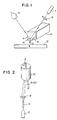
- a stylus-cantilever system includes a cantilever beam 10 made of, e.g., silicon or silicon nitride, having a tip 12 of a length in the range between 1 and 10 microns, and preferably 5 micrometers in length disposed at the end of a pair of supporting arms 14. Alternatively, the tip 12 can be disposed at the end of single supporting arm extending from end of cantilever beam 10.
- a laser 18 transmits a laser beam through lens 20 where the beam is focussed directly onto the back of the arms 14 in the region of the tip.
- the laser beam is focussed onto the back of the cantilever beam; or, alternatively, onto a reflector 16 attached to the back of the cantilever beam for the purpose of enhancing reflective properties.
- the term "onto the back of the cantilever” will be understood to mean a laser beam transmitted onto the back of the cantilever beam itself, onto the back of a reflector coupled to the back of the cantilever beam, or onto one or more tip supporting arms in the region of the tip.
- the laser beam is reflected onto a position-sensitive detector 22.
- the output of the detector 22 is provided as one input to a general purpose computer.
- the x-axis and y-axis positions of the tip as the tip is scanned over the workpiece surface are also provided as inputs to the computer as is known in the art.
- the computer processes the data in a known manner for providing a topographical image of the surface at atomic resolution.
- the image can be displayed on a screen or on a strip chart, be in tabular form or otherwise provided in a visual format.
- the laser 18 is a compact single-mode diode laser operating preferably in the visible light spectrum, preferably at 670 nm, for ease of alignment. However, a laser operating in the infrared or ultraviolet range will perform equally as well.
- the preferred position-sensitive detector is a silicon bicell.
- an atomic force microscope detects the motion of the tip toward and away from a surface to be inspected 24.
- the motion of the tip is proportional to the interaction force between the tip and surface of the workpiece w.
- the orientation of the cantilever beam supporting the tip is measured.
- the measurements can be performed in a vacuum or ultrahigh vacuum, in an aqueous environment or in air depending upon the application.
- the general atomic force microscope configuration for each environment is well known to those skilled in the art.
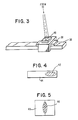
- Figure 2 illustrates a modification to a conventional atomic force microscope which is most useful when performing measurements in an ultrahigh vacuum environment. However, the microscope will perform in water and in non-vacuum environments equally as well with the modification.
- the laser beam from laser 18 is coupled to a single mode optical fiber 26 whose output is focussed via lens 28 to a reflector 30 disposed on the back of a cantilever beam.
- the laser beam is reflected from the reflector to a position sensitive detector.
- the side of the cantilever beam including the tip is referred to as the front side of the cantilever beam and the oppositely disposed side of the cantilever beam containing the reflector is referred to as the back of the cantilever beam.
- a piezoelectric tube 32 is used as a scanner.
- the cantilever beam which is micromachined, has a length in the range between 100 and 200 microns and preferably is 100 microns long, and has a width in the range between 5 and 30 microns and preferably is 20 microns wide.
- the length and width dimensions are dependent upon the material comprising the cantilever beam and are selected in order to achieve a soft lever configuration of the stylus-cantilever system having a force constant in the range between 0.01 and 100 Newton/meter and preferably having a force constant of 0.1 N/m.
- the cantilever beam is coupled to the tube scanner 32.
- micromachined cantilever beam of small dimension enables imaging at atomic resolution as contrasted with the heretofore employed cantilever beams which were typically on the order of one millimeter in length and were limited in terms of resolution.
- the described arrangement ensures a high scanning speed and imposes virtually no restriction on the size of a surface to be investigated.
- the maximum scanning speed is determined by the resonance frequency of the cantilever beam, typically 100 kHz, or by the resonance frequency of the tube scanner, typically 10 kHz.
- a preferred position sensitive detector is a bicell and preferably a silicon bicell for detecting the angle of deflection of the laser beam.
- An inertial mover as shown in Figure 3, ensures the rejection of intensity fluctuations of the light falling on the bicell by remotely positioning the bicell symmetrically with respect to the laser beam deflected from the cantilever beam.
- the inertial mover includes a piezoelectric bar 36 whose length is varied by the application of a saw-tooth waveform voltage signal to the bar as is known in the art.
- a piezoelectric bar 36 mounteded on a sapphire plate 38 located near one end of the piezoelectric bar 36 is a bicell 40.
- the bicell can readily slide responsive to an appropriate saw-tooth waveform voltage signal applied to the piezoelectric bar 36 via conductors (not shown) as is known in the art.
- the sapphire plate 38 and the bicell 40 coupled thereto will move as the saw-toothed waveform voltage signal is applied to the bar. In this manner, the position of the bicell 40 can be remotely controlled in steps as small as 10 nm.
- the inertial mover is compact and fully computer-controllable which is particularly advantageous for use in ultrahigh vacuum environments.
- the optical fiber 26 can be eliminated in order to provide a more compact design. It is possible to eliminate the inertial mover when operating in a non-vacuum environment.
- a primary function of the inertial mover is to provide the ability to remotely position the bicell in a vacuum chamber. For example, in situ tip replacement can be incorporated in the atomic force microscope design, a feature that could result in significant misalignment of the optical path requiring repositioning of the bicell.
- the output of a visible diode laser is an elliptical beam having an aspect ratio in the range of approximately 5 to 7:1.
- the ellipticity is eliminated by the use of suitable optics.
- the asymmetric beam shape is an important aspect of an alternative preferred embodiment of the invention.
- the elliptical beam spot reflects from the cantilever beam in accordance with the same aspect ratio and the resultant reflected spot size is approximately six times smaller in the direction perpendicular to the longitudinal axis of the cantilever beam.
- the size of the reflected laser beam 46 received at the bicell 40 is 5 to 7 times larger in the direction perpendicular to the deflection direction as shown in Figure 5, thereby enabling the use of higher laser power, without exceeding the saturation limit of the bicell, and correspondingly achieving higher measurement sensitivity.
- the distance between the cantilever beam and bicell can be decreased, thus resulting in an even more compact microscope.
Landscapes
- Chemical & Material Sciences (AREA)
- Nuclear Medicine, Radiotherapy & Molecular Imaging (AREA)
- Engineering & Computer Science (AREA)
- Nanotechnology (AREA)
- Physics & Mathematics (AREA)
- Health & Medical Sciences (AREA)
- General Health & Medical Sciences (AREA)
- General Physics & Mathematics (AREA)
- Radiology & Medical Imaging (AREA)
- Crystallography & Structural Chemistry (AREA)
- Analytical Chemistry (AREA)
- Length Measuring Devices With Unspecified Measuring Means (AREA)
- Length Measuring Devices By Optical Means (AREA)
Claims (11)
- Kraftmikroskop zur Erzeugung einer topographischen Abbildung der Oberfläche einer Probe (24) miteiner an einem Ende der Vorderseite eines mikromechanisch gefertigten, einseitig festgelegten Trägerarmes (10) befestigten Spitze (12), die geeignet ist, in der Nähe der Oberfläche einer Probe positioniert zu werden, wobei die Kräfte zwischen den Atomen der Spitze und der Oberfläche den einseitig festgelegten Trägerarm auslenken,Lasermitteln (18) zum Einstrahlen eines Laserstrahls auf die Rückseite des einseitig festgelegten Trägerarmesund positionsempfindlichen Detektionsmitteln (22) zum Empfangen des Laserstrahls, nachdem er von dem einseitig festgelegten Trägerarm reflektiert wurde und zum Umwandeln des reflektierten Strahles in ein Ausgangssignal, dadurch gekennzeichnet, daßdas Ausgangssignal der positionsempfindlichen Detektionsmittel (22) die Position anzeigt, bei welcher der reflektierte Strahl auf die positionsempfindlichen Detektionsmittel auftrifft,und die Lasermittel (19) sowie die positionsempfindlichen Detektionsmittel (22) bezüglich des einseitig festgelegten Trägerarmes (10) so angeordnet sind, daß das Ausgangssignal die Lage des einseitig festgelegten Trägerarmes (10) anzeigt,dadurch gekennzeichnet, daß die Lasermittel (18) einen Laserstrahl (42), der eine elliptische Gestalt hat, auf die Rückseite (44) des einseitig festgelegten Trägerarmes (10) aufstrahlen.
- Kraftmikroskop nach Anspruch 1, wobei die Lasermittel (18) eine optische Faser (26) beinhalten, um den Laserstrahl zu dem einseitig festgelegten Trägerarm (10) zu führen.
- Kraftmikroskop nach Anspruch 1 oder 2, das desweiteren Reflektionsmittel (16) beinhaltet, die an die Rückseite des einseitig festgelegten Trägerarms angekoppelt sind, um den eingestrahlten Laserstrahl zu reflektieren.
- Kraftmikroskop nach Anspruch 1, 2 oder 3, wobei die Spitze (12) mittels wenigstens eines Armes (14) an dem mikromechanisch gefertigten, einseitig festgelegten Trägerarm (10) befestigt ist und die Lasermittel (18) einen Laserstrahl auf den wenigstens einen Arm im Bereich der Spitze einstrahlen.
- Kraftmikroskop nach einem der vorhergehenden Ansprüche, wobei die positionsempfindlichen Detektionsmittel (22) eine Doppelzelle (40) beinhalten, vorzugsweise eine Doppelzelle aus Silizium.
- Kraftmikroskop nach einem der vorhergehenden Ansprüche, wobei die Lasermittel (18) einen Diodenlaser oder einen Einmoden-Diodenlaser beinhalten.
- Kraftmikroskop nach einem der vorhergehenden Ansprüche, wobei die positionsempfindlichen Detektionsmittel (22) aus der Entfernung positionierbar sind, vorzugsweise mittels einer Trägheitsantriebsvorrichtung (36).
- Kraftmikroskop nach einem der vorhergehenden Ansprüche, wobei die Spitze (12) und die positionsempfindlichen Detektionsmittel (22) in einer unzugänglichen Umgebung, wie einem Vakuum oder einem Ultrahochvakuum, angeordnet sind.
- Kraftmikroskop nach einem der vorhergehenden Ansprüche 1 bis 8, wobei der Laserstrahl (46), der von den positionsempfindlichen Detektionsmitteln (40) empfangen wird, eine elliptische Gestalt hat.
- Kraftmikroskop nach Anspruch 9, wobei der Laserstrahl (46), der von den positionsempfindlichen Mitteln (40) empfangen wird, ein Verhältnis im Bereich von etwa 5 bis 7:1 in den Detektionsmitteln hat.
- Verfahren zum Erzeugen einer topographischen Abbildung der Oberfläche einer Probe (24) durch Verwenden eines Kraftmikroskopes nach einem der vorhergehenden Ansprüche.
Applications Claiming Priority (2)
| Application Number | Priority Date | Filing Date | Title |
|---|---|---|---|
| US588795 | 1984-03-12 | ||
| US07/588,795 US5144833A (en) | 1990-09-27 | 1990-09-27 | Atomic force microscopy |
Publications (2)
| Publication Number | Publication Date |
|---|---|
| EP0480136A1 EP0480136A1 (de) | 1992-04-15 |
| EP0480136B1 true EP0480136B1 (de) | 1996-09-25 |
Family
ID=24355333
Family Applications (1)
| Application Number | Title | Priority Date | Filing Date |
|---|---|---|---|
| EP91112362A Expired - Lifetime EP0480136B1 (de) | 1990-09-27 | 1991-07-24 | Atomkraft-Mikroskopie |
Country Status (4)
| Country | Link |
|---|---|
| US (2) | US5144833A (de) |
| EP (1) | EP0480136B1 (de) |
| JP (1) | JP2516292B2 (de) |
| DE (1) | DE69122343T2 (de) |
Families Citing this family (70)
| Publication number | Priority date | Publication date | Assignee | Title |
|---|---|---|---|---|
| US5157251A (en) * | 1991-03-13 | 1992-10-20 | Park Scientific Instruments | Scanning force microscope having aligning and adjusting means |
| EP0511662B1 (de) * | 1991-04-30 | 1996-07-10 | Matsushita Electric Industrial Co., Ltd. | Raster-Abtastmikroskop, molekulares Verarbeitungsverfahren unter Verwendung des Mikroskops und Verfahren zum Wahrnehmen der DNA-Basen-Anordnung |
| US5155361A (en) * | 1991-07-26 | 1992-10-13 | The Arizona Board Of Regents, A Body Corporate Acting For And On Behalf Of Arizona State University | Potentiostatic preparation of molecular adsorbates for scanning probe microscopy |
| JPH0540034A (ja) * | 1991-08-08 | 1993-02-19 | Nikon Corp | 複合型顕微鏡 |
| US5298975A (en) * | 1991-09-27 | 1994-03-29 | International Business Machines Corporation | Combined scanning force microscope and optical metrology tool |
| US5537372A (en) * | 1991-11-15 | 1996-07-16 | International Business Machines Corporation | High density data storage system with topographic contact sensor |
| DE69309318T2 (de) * | 1992-01-10 | 1997-10-30 | Hitachi, Ltd., Tokio/Tokyo | Verfahren und Vorrichtung zum Beobachten einer Fläche |
| US5291775A (en) * | 1992-03-04 | 1994-03-08 | Topometrix | Scanning force microscope with integrated optics and cantilever mount |
| US5448399A (en) * | 1992-03-13 | 1995-09-05 | Park Scientific Instruments | Optical system for scanning microscope |
| US5376790A (en) * | 1992-03-13 | 1994-12-27 | Park Scientific Instruments | Scanning probe microscope |
| JP3000500B2 (ja) * | 1992-09-02 | 2000-01-17 | セイコーインスツルメンツ株式会社 | 原子間力顕微鏡 |
| JP2704601B2 (ja) * | 1993-04-12 | 1998-01-26 | セイコーインスツルメンツ株式会社 | 走査型近視野原子間力顕微鏡、及びその顕微鏡に使用されるプローブ、及びそのプローブの製造方法 |
| US5463897A (en) * | 1993-08-17 | 1995-11-07 | Digital Instruments, Inc. | Scanning stylus atomic force microscope with cantilever tracking and optical access |
| US5450746A (en) * | 1993-10-12 | 1995-09-19 | The University Of North Carolina | Constant force stylus profiling apparatus and method |
| US5388452A (en) * | 1993-10-15 | 1995-02-14 | Quesant Instrument Corporation | Detection system for atomic force microscopes |
| US5416327A (en) * | 1993-10-29 | 1995-05-16 | Regents Of The University Of California | Ultrafast scanning probe microscopy |
| US5410910A (en) * | 1993-12-22 | 1995-05-02 | University Of Virginia Patent Foundation | Cryogenic atomic force microscope |
| US5440920A (en) * | 1994-02-03 | 1995-08-15 | Molecular Imaging Systems | Scanning force microscope with beam tracking lens |
| US5866805A (en) * | 1994-05-19 | 1999-02-02 | Molecular Imaging Corporation Arizona Board Of Regents | Cantilevers for a magnetically driven atomic force microscope |
| US5515719A (en) * | 1994-05-19 | 1996-05-14 | Molecular Imaging Corporation | Controlled force microscope for operation in liquids |
| US5513518A (en) * | 1994-05-19 | 1996-05-07 | Molecular Imaging Corporation | Magnetic modulation of force sensor for AC detection in an atomic force microscope |
| US5753814A (en) * | 1994-05-19 | 1998-05-19 | Molecular Imaging Corporation | Magnetically-oscillated probe microscope for operation in liquids |
| JP3229914B2 (ja) * | 1994-12-12 | 2001-11-19 | 日本電子株式会社 | 走査型プローブ顕微鏡 |
| US5675154A (en) * | 1995-02-10 | 1997-10-07 | Molecular Imaging Corporation | Scanning probe microscope |
| US5621210A (en) * | 1995-02-10 | 1997-04-15 | Molecular Imaging Corporation | Microscope for force and tunneling microscopy in liquids |
| US5750989A (en) * | 1995-02-10 | 1998-05-12 | Molecular Imaging Corporation | Scanning probe microscope for use in fluids |
| DE19504855A1 (de) * | 1995-02-15 | 1996-08-22 | Basf Ag | Verfahren zur chemisch differenzierenden Abbildung mittels Rasterkraftmikroskopie |
| US5874668A (en) * | 1995-10-24 | 1999-02-23 | Arch Development Corporation | Atomic force microscope for biological specimens |
| US5654546A (en) * | 1995-11-07 | 1997-08-05 | Molecular Imaging Corporation | Variable temperature scanning probe microscope based on a peltier device |
| US5821545A (en) * | 1995-11-07 | 1998-10-13 | Molecular Imaging Corporation | Heated stage for a scanning probe microscope |
| US5834644A (en) * | 1995-11-13 | 1998-11-10 | The University Of Virginia Patent Foundation | Automatic atomic force microscope with piezotube scanner |
| US5812266A (en) * | 1995-12-15 | 1998-09-22 | Hewlett-Packard Company | Non-contact position sensor |
| US5886787A (en) * | 1995-12-15 | 1999-03-23 | Hewlett-Packard Company | Displacement sensor and method for producing target feature thereof |
| US6118124A (en) * | 1996-01-18 | 2000-09-12 | Lockheed Martin Energy Research Corporation | Electromagnetic and nuclear radiation detector using micromechanical sensors |
| US5908981A (en) * | 1996-09-05 | 1999-06-01 | Board Of Trustees Of The Leland Stanford, Jr. University | Interdigital deflection sensor for microcantilevers |
| US5825020A (en) * | 1996-09-06 | 1998-10-20 | The Regents Of The University Of California | Atomic force microscope for generating a small incident beam spot |
| US5866806A (en) * | 1996-10-11 | 1999-02-02 | Kla-Tencor Corporation | System for locating a feature of a surface |
| US6459492B1 (en) | 1997-03-14 | 2002-10-01 | Agilent Technologies, Inc. | Non-contact position sensor |
| JP4020216B2 (ja) * | 1997-03-14 | 2007-12-12 | アジレント・テクノロジーズ・インク | 非接触位置センサ |
| US5861550A (en) | 1997-10-14 | 1999-01-19 | Raymax Technology, Incorporated | Scanning force microscope |
| US5874669A (en) * | 1997-10-16 | 1999-02-23 | Raymax Technology, Inc. | Scanning force microscope with removable probe illuminator assembly |
| US6138503A (en) * | 1997-10-16 | 2000-10-31 | Raymax Technology, Inc. | Scanning probe microscope system including removable probe sensor assembly |
| US6437343B1 (en) * | 1998-03-13 | 2002-08-20 | Olympus Optical Co., Ltd. | Scanner system and piezoelectric micro-inching mechansim used in scanning probe microscope |
| US6050722A (en) * | 1998-03-25 | 2000-04-18 | Thundat; Thomas G. | Non-contact passive temperature measuring system and method of operation using micro-mechanical sensors |
| US5992226A (en) * | 1998-05-08 | 1999-11-30 | The United States Of America As Represented By The Secretary Of The Navy | Apparatus and method for measuring intermolecular interactions by atomic force microscopy |
| US6489611B1 (en) | 1998-10-07 | 2002-12-03 | Massachusetts Institute Of Technology | Atomic force microscope for profiling high aspect ratio samples |
| US5958701A (en) * | 1999-01-27 | 1999-09-28 | The United States Of America As Represented By The Secretary Of The Navy | Method for measuring intramolecular forces by atomic force |
| JP2003507723A (ja) * | 1999-08-19 | 2003-02-25 | ザ・リージェンツ・オブ・ザ・ユニバーシティー・オブ・カリフォルニア | カンチレバーアレイブロックのパレットにより微小力を可視的に識別する装置及び方法 |
| JP4843844B2 (ja) * | 1999-12-27 | 2011-12-21 | ソニー株式会社 | 光ヘッド、受発光素子、及び光記録媒体記録再生装置 |
| US6642517B1 (en) | 2000-01-25 | 2003-11-04 | Veeco Instruments, Inc. | Method and apparatus for atomic force microscopy |
| US6479820B1 (en) | 2000-04-25 | 2002-11-12 | Advanced Micro Devices, Inc. | Electrostatic charge reduction of photoresist pattern on development track |
| US6587600B1 (en) * | 2000-08-15 | 2003-07-01 | Floor Corporation | Methods and apparatus for producing topocompositional images |
| US6871527B2 (en) * | 2001-07-18 | 2005-03-29 | The Regents Of The University Of California | Measurement head for atomic force microscopy and other applications |
| US20030154149A1 (en) * | 2002-02-13 | 2003-08-14 | Dilip Gajendragadkar | System and method of creating and executing a restricted stock sale plan |
| US6912892B2 (en) * | 2002-04-30 | 2005-07-05 | Hewlett-Packard Development Company, L.P. | Atomic force microscope |
| US7041963B2 (en) * | 2003-11-26 | 2006-05-09 | Massachusetts Institute Of Technology | Height calibration of scanning probe microscope actuators |
| US7230719B2 (en) * | 2003-12-02 | 2007-06-12 | National University Of Singapore | High sensitivity scanning probe system |
| JP4596813B2 (ja) * | 2004-04-21 | 2010-12-15 | 独立行政法人科学技術振興機構 | 量子線支援原子間力顕微法および量子線支援原子間力顕微鏡 |
| US7205237B2 (en) * | 2005-07-05 | 2007-04-17 | International Business Machines Corporation | Apparatus and method for selected site backside unlayering of si, GaAs, GaxAlyAszof SOI technologies for scanning probe microscopy and atomic force probing characterization |
| US20100294927A1 (en) * | 2005-09-12 | 2010-11-25 | Nanolnk, Inc. | High throughput inspecting |
| US9189728B2 (en) | 2009-07-23 | 2015-11-17 | I-Property Holding Corp. | Method for the authentication of dosage forms |
| US8726410B2 (en) | 2010-07-30 | 2014-05-13 | The United States Of America As Represented By The Secretary Of The Air Force | Atomic force microscopy system and method for nanoscale measurement |
| ITTO20120692A1 (it) * | 2012-08-02 | 2014-02-03 | Microla Optoelectronics S R L | Sistema di misura a struttura oscillante |
| US9383386B2 (en) | 2013-03-14 | 2016-07-05 | Oxford Instruments Asylum Research, Inc. | Optical beam positioning unit for atomic force microscope |
| US9804193B2 (en) | 2014-03-12 | 2017-10-31 | Oxford Instruments Asylum Research, Inc | Metrological scanning probe microscope |
| US10705114B2 (en) | 2014-03-12 | 2020-07-07 | Oxford Instruments Asylum Research Inc | Metrological scanning probe microscope |
| DE102014010417A1 (de) * | 2014-07-14 | 2016-01-14 | Nanosurf Ag | Positionsmesssystem für den Nanometerbereich |
| JP6588278B2 (ja) * | 2015-09-01 | 2019-10-09 | 株式会社日立ハイテクサイエンス | 走査プローブ顕微鏡および走査プローブ顕微鏡の光軸調整方法 |
| CN106353535A (zh) * | 2016-10-10 | 2017-01-25 | 中国科学院深圳先进技术研究院 | 原位光电多功能耦合原子力显微镜测试系统 |
| CN111811939B (zh) * | 2020-07-21 | 2022-08-02 | 上海交通大学 | 超低温环境下的高精度纳米力学检测系统 |
Family Cites Families (47)
| Publication number | Priority date | Publication date | Assignee | Title |
|---|---|---|---|---|
| US1976337A (en) * | 1931-03-06 | 1934-10-09 | Floyd A Firestone | Apparatus for determining roughness of surfaces |
| US2048154A (en) * | 1935-05-27 | 1936-07-21 | Univ Michigan | Apparatus for determining roughness of surfaces |
| US2171433A (en) * | 1937-02-09 | 1939-08-29 | Electronic Controls Corp | Smoothness gauge |
| US2205517A (en) * | 1938-03-31 | 1940-06-25 | Pittsburgh Plate Glass Co | Profilograph |
| US2686101A (en) * | 1951-06-11 | 1954-08-10 | John E Davis | Apparatus and method for reproducing surface contours |
| US3251135A (en) * | 1962-07-09 | 1966-05-17 | Rank Precision Ind Ltd | Apparatus for measuring or indicating lack of straightness of a surface |
| CA836137A (en) * | 1963-05-03 | 1970-03-03 | Westinghouse Electric Corporation | Current responsive apparatus for high voltage circuits |
| US3571579A (en) * | 1968-04-25 | 1971-03-23 | Rank Organisation Ltd | Assessing of surface profiles |
| DE1937465A1 (de) * | 1968-07-24 | 1970-04-09 | Konishiroku Photo Ind | Vorrichtung zum Feststellen kleinster Neigungen eines Objektes gegenueber einer Ebene |
| AT353497B (de) * | 1972-05-23 | 1979-11-12 | Leitz Ernst Gmbh | Vorrichtung an mikroskopen, zum automatischen fokussieren des geraetes auf unterschiedliche objekt-ebenen |
| US3782205A (en) * | 1972-11-09 | 1974-01-01 | Nasa | Temperature compensated digital inertial sensor |
| US4102577A (en) * | 1977-01-04 | 1978-07-25 | Fuji Photo Optical Co., Ltd. | Method of forming moire contour lines |
| US4267732A (en) * | 1978-11-29 | 1981-05-19 | Stanford University Board Of Trustees | Acoustic microscope and method |
| US4596925A (en) * | 1982-10-27 | 1986-06-24 | The Foxboro Company | Fiber optic displacement sensor with built-in reference |
| FR2554224B1 (fr) * | 1983-10-27 | 1987-08-28 | Telecommunications Sa | Systeme de reperage de la position angulaire d'un dispositif mecanique |
| GB8415128D0 (en) * | 1984-06-14 | 1984-07-18 | Chaimowicz J C A | Optical displacement sensors |
| JPH0629964B2 (ja) * | 1984-09-11 | 1994-04-20 | 株式会社ニコン | マーク検出方法 |
| JPS61133843A (ja) * | 1984-12-05 | 1986-06-21 | Hitachi Electronics Eng Co Ltd | 表面検査装置 |
| US4782239A (en) * | 1985-04-05 | 1988-11-01 | Nippon Kogaku K. K. | Optical position measuring apparatus |
| JPH0713707B2 (ja) * | 1985-04-26 | 1995-02-15 | オリンパス光学工業株式会社 | 走査型光学顕微鏡 |
| JPH0726806B2 (ja) * | 1985-06-13 | 1995-03-29 | 株式会社日立製作所 | 距離測定装置 |
| USRE33387E (en) * | 1985-11-26 | 1990-10-16 | International Business Machines Corporation | Atomic force microscope and method for imaging surfaces with atomic resolution |
| US4724318A (en) * | 1985-11-26 | 1988-02-09 | International Business Machines Corporation | Atomic force microscope and method for imaging surfaces with atomic resolution |
| JPS62156515A (ja) * | 1985-12-27 | 1987-07-11 | Mitsubishi Electric Corp | 変位測定装置 |
| EP0262253A1 (de) * | 1986-10-03 | 1988-04-06 | International Business Machines Corporation | Mikromechanische Fühlervorrichtung für atomare Kräfte |
| US4800274A (en) * | 1987-02-02 | 1989-01-24 | The Regents Of The University Of California | High resolution atomic force microscope |
| US4762996A (en) * | 1987-04-20 | 1988-08-09 | International Business Machines Corporation | Coarse approach positioning device |
| EP0290647B1 (de) * | 1987-05-12 | 1991-07-24 | International Business Machines Corporation | Atomares Kräftemikroskop mit oscillierendem Quarz |
| JPS63304103A (ja) * | 1987-06-05 | 1988-12-12 | Hitachi Ltd | 走査表面顕微鏡 |
| JPS643502A (en) * | 1987-06-25 | 1989-01-09 | Seiko Instr & Electronics | Scanning type tunnel microscope |
| US4823004A (en) * | 1987-11-24 | 1989-04-18 | California Institute Of Technology | Tunnel and field effect carrier ballistics |
| FR2624600B1 (fr) * | 1987-12-09 | 1990-04-13 | Snecma | Procede et dispositif de controle de contours geometriques sans contact |
| US4906840A (en) * | 1988-01-27 | 1990-03-06 | The Board Of Trustees Of Leland Stanford Jr., University | Integrated scanning tunneling microscope |
| US4861990A (en) * | 1988-02-09 | 1989-08-29 | California Institute Of Technology | Tunneling susceptometry |
| US4878114A (en) * | 1988-05-10 | 1989-10-31 | University Of Windsor | Method and apparatus for assessing surface roughness |
| US4889988A (en) * | 1988-07-06 | 1989-12-26 | Digital Instruments, Inc. | Feedback control for scanning tunnel microscopes |
| US4894537A (en) * | 1988-07-21 | 1990-01-16 | Canadian Patents & Development Ltd. | High stability bimorph scanning tunneling microscope |
| US4873401A (en) * | 1988-09-19 | 1989-10-10 | Bendix Electronics Limited | Electromagnetic damped inertia sensor |
| US4827091A (en) * | 1988-09-23 | 1989-05-02 | Automotive Systems Laboratory, Inc. | Magnetically-damped, testable accelerometer |
| US5018865A (en) * | 1988-10-21 | 1991-05-28 | Ferrell Thomas L | Photon scanning tunneling microscopy |
| US4896044A (en) * | 1989-02-17 | 1990-01-23 | Purdue Research Foundation | Scanning tunneling microscope nanoetching method |
| US4935634A (en) * | 1989-03-13 | 1990-06-19 | The Regents Of The University Of California | Atomic force microscope with optional replaceable fluid cell |
| US5015850A (en) * | 1989-06-20 | 1991-05-14 | The Board Of Trustees Of The Leland Stanford Junior University | Microfabricated microscope assembly |
| EP0413042B1 (de) * | 1989-08-16 | 1992-12-16 | International Business Machines Corporation | Verfahren für die Herstellung mikromechanischer Messfühler für AFM/STM-Profilometrie und mikromechanischer Messfühlerkopf |
| US5003815A (en) * | 1989-10-20 | 1991-04-02 | International Business Machines Corporation | Atomic photo-absorption force microscope |
| US4992728A (en) * | 1989-12-21 | 1991-02-12 | International Business Machines Corporation | Electrical probe incorporating scanning proximity microscope |
| US5053588A (en) * | 1990-02-20 | 1991-10-01 | Trw Technar Inc. | Calibratable crash sensor |
-
1990
- 1990-09-27 US US07/588,795 patent/US5144833A/en not_active Ceased
-
1991
- 1991-07-24 EP EP91112362A patent/EP0480136B1/de not_active Expired - Lifetime
- 1991-07-24 DE DE69122343T patent/DE69122343T2/de not_active Expired - Lifetime
- 1991-08-27 JP JP3238906A patent/JP2516292B2/ja not_active Expired - Fee Related
-
1997
- 1997-01-27 US US08/791,445 patent/USRE37299E1/en not_active Expired - Lifetime
Also Published As
| Publication number | Publication date |
|---|---|
| US5144833A (en) | 1992-09-08 |
| EP0480136A1 (de) | 1992-04-15 |
| DE69122343T2 (de) | 1997-04-10 |
| JPH04233404A (ja) | 1992-08-21 |
| DE69122343D1 (de) | 1996-10-31 |
| USRE37299E1 (en) | 2001-07-31 |
| JP2516292B2 (ja) | 1996-07-24 |
Similar Documents
| Publication | Publication Date | Title |
|---|---|---|
| EP0480136B1 (de) | Atomkraft-Mikroskopie | |
| US5298975A (en) | Combined scanning force microscope and optical metrology tool | |
| EP0410131B1 (de) | Nah-Feld Lorentz-Kraft-Mikroskopie | |
| US6196061B1 (en) | AFM with referenced or differential height measurement | |
| US5388452A (en) | Detection system for atomic force microscopes | |
| US5253516A (en) | Atomic force microscope for small samples having dual-mode operating capability | |
| US6530268B2 (en) | Apparatus and method for isolating and measuring movement in a metrology apparatus | |
| EP0394962B1 (de) | Atomkraftmikroskop | |
| US8528110B2 (en) | Probe detection system | |
| US5324935A (en) | Scanning probe microscope having a directional coupler and a Z-direction distance adjusting piezoelectric element | |
| US6910368B2 (en) | Removable probe sensor assembly and scanning probe microscope | |
| US6642517B1 (en) | Method and apparatus for atomic force microscopy | |
| EP0387906A2 (de) | Sensor mit freitragendem Ausleger | |
| EP0712533B1 (de) | Sondenmikroskopie | |
| US20030209060A1 (en) | Apparatus and method for isolating and measuring movement in metrology apparatus | |
| JPH03296612A (ja) | 原子間力顕微鏡 | |
| JPH07198359A (ja) | 微動機構及び走査型プローブ顕微鏡 | |
| JPH06258068A (ja) | 原子間力顕微鏡 | |
| KR100298301B1 (ko) | 굴곡센서를 내장한 스캐닝 프로브 및 이를 이용한 굴곡측정장치 | |
| JPH03259709A (ja) | 原子間力測定顕微鏡 | |
| JPH04162341A (ja) | 試料表面の像形成方法及びその装置 | |
| JPH08201463A (ja) | 表面電荷測定器 | |
| JPH06258067A (ja) | 原子間力顕微鏡 |
Legal Events
| Date | Code | Title | Description |
|---|---|---|---|
| PUAI | Public reference made under article 153(3) epc to a published international application that has entered the european phase |
Free format text: ORIGINAL CODE: 0009012 |
|
| AK | Designated contracting states |
Kind code of ref document: A1 Designated state(s): DE FR GB |
|
| 17P | Request for examination filed |
Effective date: 19920817 |
|
| 17Q | First examination report despatched |
Effective date: 19931013 |
|
| GRAH | Despatch of communication of intention to grant a patent |
Free format text: ORIGINAL CODE: EPIDOS IGRA |
|
| GRAH | Despatch of communication of intention to grant a patent |
Free format text: ORIGINAL CODE: EPIDOS IGRA |
|
| GRAA | (expected) grant |
Free format text: ORIGINAL CODE: 0009210 |
|
| AK | Designated contracting states |
Kind code of ref document: B1 Designated state(s): DE FR GB |
|
| REF | Corresponds to: |
Ref document number: 69122343 Country of ref document: DE Date of ref document: 19961031 |
|
| ET | Fr: translation filed | ||
| PGFP | Annual fee paid to national office [announced via postgrant information from national office to epo] |
Ref country code: FR Payment date: 19970707 Year of fee payment: 7 |
|
| PLBE | No opposition filed within time limit |
Free format text: ORIGINAL CODE: 0009261 |
|
| STAA | Information on the status of an ep patent application or granted ep patent |
Free format text: STATUS: NO OPPOSITION FILED WITHIN TIME LIMIT |
|
| 26N | No opposition filed | ||
| PG25 | Lapsed in a contracting state [announced via postgrant information from national office to epo] |
Ref country code: FR Free format text: LAPSE BECAUSE OF NON-PAYMENT OF DUE FEES Effective date: 19990331 |
|
| REG | Reference to a national code |
Ref country code: FR Ref legal event code: ST |
|
| REG | Reference to a national code |
Ref country code: GB Ref legal event code: IF02 |
|
| REG | Reference to a national code |
Ref country code: GB Ref legal event code: 746 Effective date: 20090619 |
|
| PGFP | Annual fee paid to national office [announced via postgrant information from national office to epo] |
Ref country code: DE Payment date: 20100722 Year of fee payment: 20 |
|
| PGFP | Annual fee paid to national office [announced via postgrant information from national office to epo] |
Ref country code: GB Payment date: 20100719 Year of fee payment: 20 |
|
| REG | Reference to a national code |
Ref country code: DE Ref legal event code: R071 Ref document number: 69122343 Country of ref document: DE |
|
| REG | Reference to a national code |
Ref country code: DE Ref legal event code: R071 Ref document number: 69122343 Country of ref document: DE |
|
| REG | Reference to a national code |
Ref country code: GB Ref legal event code: PE20 Expiry date: 20110723 |
|
| PG25 | Lapsed in a contracting state [announced via postgrant information from national office to epo] |
Ref country code: GB Free format text: LAPSE BECAUSE OF EXPIRATION OF PROTECTION Effective date: 20110723 |
|
| PG25 | Lapsed in a contracting state [announced via postgrant information from national office to epo] |
Ref country code: DE Free format text: LAPSE BECAUSE OF EXPIRATION OF PROTECTION Effective date: 20110725 |