EP0483833A1 - Dispositif de circuit intégré semi-conducteur comprenant des cellules ayant un terminal auto-verrouillant - Google Patents
Dispositif de circuit intégré semi-conducteur comprenant des cellules ayant un terminal auto-verrouillant Download PDFInfo
- Publication number
- EP0483833A1 EP0483833A1 EP91118570A EP91118570A EP0483833A1 EP 0483833 A1 EP0483833 A1 EP 0483833A1 EP 91118570 A EP91118570 A EP 91118570A EP 91118570 A EP91118570 A EP 91118570A EP 0483833 A1 EP0483833 A1 EP 0483833A1
- Authority
- EP
- European Patent Office
- Prior art keywords
- cell
- clamping
- basic gate
- circuit device
- level signal
- Prior art date
- Legal status (The legal status is an assumption and is not a legal conclusion. Google has not performed a legal analysis and makes no representation as to the accuracy of the status listed.)
- Granted
Links
Images


Classifications
-
- H—ELECTRICITY
- H10—SEMICONDUCTOR DEVICES; ELECTRIC SOLID-STATE DEVICES NOT OTHERWISE PROVIDED FOR
- H10D—INORGANIC ELECTRIC SEMICONDUCTOR DEVICES
- H10D89/00—Aspects of integrated devices not covered by groups H10D84/00 - H10D88/00
- H10D89/10—Integrated device layouts
-
- H—ELECTRICITY
- H10—SEMICONDUCTOR DEVICES; ELECTRIC SOLID-STATE DEVICES NOT OTHERWISE PROVIDED FOR
- H10D—INORGANIC ELECTRIC SEMICONDUCTOR DEVICES
- H10D84/00—Integrated devices formed in or on semiconductor substrates that comprise only semiconducting layers, e.g. on Si wafers or on GaAs-on-Si wafers
- H10D84/90—Masterslice integrated circuits
Definitions
- the present invention relates to a semiconductor integrated circuit device and, more particularly, to an LSI of CPU core type standard cell custom.
- custom LSI of CPU core type enables a user to construct a microcomputer suited to a desired purpose by freely and selectively combining logic functions of large scale cells provided in advance such as CPU, ROM, RAM, I/O port, serial I/O and timers, and combining gate cells provided in advance by the LSI makers.
- microcomputer is hereinafter referred to as a "custom microcomputer”.
- EWS Engineer Work Station
- Fig. 1 shows the symbolic diagram on the EWS where the 5-input NAND is used for a 4-input NAND circuit.
- the numeral 11 represents the symbol designating the 5-input NAND.
- the numeral 12 represents the symbol designating a basic gate cell for clamping in the EWS, having a terminal CLH and a terminal CLL. From the terminal CLH and the terminal CLL, a high level signal and a low level signal are constantly being outputted, respectively.
- the terminal CLH of the basic gate cell 12 for clamping and the terminal A5 of the NAND circuit 11 are connected with each other for the circuit to be a 4-input NAND circuit with the four input terminals A1 ⁇ A4 being used.
- the circuit wherein a mask is laid-out based on the circuit diagram as explained above must be equipped with the basic cell for clamping and other basic gate cells which are connected to the basic cells for clamping and must have the necessary wirings for signals for clamping.
- This requires an area for accommodating such basic cell for clamping and such wirings for the other basic gate cells to be connected to the basic gate cell for clamping and this results in disadvantages due to the need of an increased area.
- the increased area requires an increased length in the wirings in the circuitry of the semiconductor circuit device and results in a delay in an operating speed of the circuit.
- a semiconductor integrated circuit device in which a desired circuit can be designed and laid-out based on cell connection information, comprising: a large scale cell arranged in advance; and a plurality of basic gate cells arranged in advance, at least either of the large scale cell and the plurality of basic gate cells having at least one clamping output terminal for constantly outputting either of a high level signal and low level signal.
- Fig. 2 shows symbols representing a circuit on the EWS for a 5-input NAND circuit 20 and Fig. 3 shows an example of mask-layout in the 5-input NAND circuit 20 of Fig. 2 as a first embodiment of the present invention.
- the symbols A1 ⁇ A5 represent input terminals formed by polysilicon layers of the 5-input NAND circuit 20, which correspond to A1 ⁇ A5 in Fig. 2, respectively.
- the symbol NO1 represents an output terminal which corresponds to the same NO1 in Fig. 2.
- the numeral 1 represents the power supply region formed in an aluminum first layer and the numeral 2 represents the ground region formed in the aluminum first layer.
- the terminal CLH which corresponds to the CLH in Fig. 2 is connected to the power supply region 1 and is constantly outputting a high level signal.
- the numeral 3 represents an aluminum second layer wiring; 4 ... represent contacts between the aluminum first layer wirings and a P-type diffusion layer; 5 ... represent contacts between aluminum first layer wirings and an N-type diffusion layer; 6 represents the P-type diffusion layer; 7 represents the N-type diffusion layer; 8 represents a through-hole connecting the aluminum first layer wiring with the aluminum second layer wiring; and 9 represents the aluminum first layer wiring.
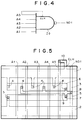
- Fig. 4 shows a circuit diagram on the EWS for the user to design a 4-input NAND circuit 20 as desired by using the symbols on the EWS circuit diagram of the 5-input NAND circuit shown in Fig. 2.
- Fig. 5 shows the mask-layout designed based on the symbolic diagram of Fig. 4. As shown in Fig. 5, the input terminal A5 is connected with the wiring layer 10 so as to realize the 4-input NAND circuit 20 as desired by the user.
- FIG. 6 shows an example of symbols on the EWS circuit for I/O port 30 among the large scale cells in a custom microcomputer as the second embodiment of the invention.
- Fig. 6 shows the I/O port 30 of 4 bits.
- P OUT0 ⁇ P OUT3 are output terminals and P IN0 ⁇ P IN3 are input terminals of the I/O port, and P CTL0 ⁇ P CTL3 are output terminals of I/O control signals for effecting a change in each bit of the I/O port between an input mode and an output mode thereof.
- a symbol A(0:3) represents an address bus of 4 bits for the I/O port and a symbol D(0:3) represents a data bus.
- An RD is an output terminal for read signals and a WR is an output terminal for write signals.
- a CLH and a CLL are output terminals for clamping signals. The terminal CLH is constantly outputting a high level signal and the terminal CLL is constantly outputting a low level signal.
- Fig. 7 shows an EWS circuit diagram in which the input terminal P IN2 and the input terminal P IN3 are clamped to a high level and a low level, respectively.
- the clamping output terminal CLH and the input terminal P IN2 are connected with each other, and the clamping terminal CLL and the input terminal P IN3 are connected with each other.
- the basic gate cells and the large scale cell themselves are equipped with the terminals for outputting clamping signals so that, where it is necessary to clamp certain terminals of the basic gate cells and the large scale cell to a fixed level, all that is necessary is to connect together such terminals for outputting the clamping signals and such input terminals as required to be clamped.
- the overall circuit area can be made small, the length of the necessary wirings in the semiconductor circuit device can also be made shorter thereby enabling the circuit to operate at a high speed.
Landscapes
- Design And Manufacture Of Integrated Circuits (AREA)
- Logic Circuits (AREA)
Applications Claiming Priority (2)
| Application Number | Priority Date | Filing Date | Title |
|---|---|---|---|
| JP292880/90 | 1990-10-30 | ||
| JP02292880A JP3084740B2 (ja) | 1990-10-30 | 1990-10-30 | 半導体集積回路 |
Publications (2)
| Publication Number | Publication Date |
|---|---|
| EP0483833A1 true EP0483833A1 (fr) | 1992-05-06 |
| EP0483833B1 EP0483833B1 (fr) | 1998-01-07 |
Family
ID=17787575
Family Applications (1)
| Application Number | Title | Priority Date | Filing Date |
|---|---|---|---|
| EP91118570A Expired - Lifetime EP0483833B1 (fr) | 1990-10-30 | 1991-10-30 | Dispositif de circuit intégré semi-conducteur comprenant des cellules ayant un terminal auto-verrouillant |
Country Status (3)
| Country | Link |
|---|---|
| EP (1) | EP0483833B1 (fr) |
| JP (1) | JP3084740B2 (fr) |
| DE (1) | DE69128609T2 (fr) |
Citations (2)
| Publication number | Priority date | Publication date | Assignee | Title |
|---|---|---|---|---|
| EP0013088A1 (fr) * | 1978-12-29 | 1980-07-09 | Fujitsu Limited | Microcircuit semiconducteur à intégration poussée |
| EP0177336A2 (fr) * | 1984-10-03 | 1986-04-09 | Fujitsu Limited | Structure intégrée de matrice de portes |
-
1990
- 1990-10-30 JP JP02292880A patent/JP3084740B2/ja not_active Expired - Fee Related
-
1991
- 1991-10-30 DE DE69128609T patent/DE69128609T2/de not_active Expired - Fee Related
- 1991-10-30 EP EP91118570A patent/EP0483833B1/fr not_active Expired - Lifetime
Patent Citations (2)
| Publication number | Priority date | Publication date | Assignee | Title |
|---|---|---|---|---|
| EP0013088A1 (fr) * | 1978-12-29 | 1980-07-09 | Fujitsu Limited | Microcircuit semiconducteur à intégration poussée |
| EP0177336A2 (fr) * | 1984-10-03 | 1986-04-09 | Fujitsu Limited | Structure intégrée de matrice de portes |
Non-Patent Citations (1)
| Title |
|---|
| PATENT ABSTRACTS OF JAPAN vol. 13, no. 307 (E-787)(3655) 13 July 1989 & JP-A-1 082 545 ( TOSHIBA K.K. ) 28 March 1989 * |
Also Published As
| Publication number | Publication date |
|---|---|
| DE69128609D1 (de) | 1998-02-12 |
| JPH04165646A (ja) | 1992-06-11 |
| JP3084740B2 (ja) | 2000-09-04 |
| EP0483833B1 (fr) | 1998-01-07 |
| DE69128609T2 (de) | 1998-07-30 |
Similar Documents
| Publication | Publication Date | Title |
|---|---|---|
| US6553450B1 (en) | Buffer to multiply memory interface | |
| EP0364925B1 (fr) | Circuit intégré à semi-conducteur comportant des entrées/sorties, permettant un test d'indépendance de connexion | |
| US4393464A (en) | Chip topography for integrated circuit communication controller | |
| EP0278857B1 (fr) | Circuit intégré du type "Masterslice" | |
| EP1548607B1 (fr) | Méthode pour fournir un microcontrôleur ayant une largeur de bus de données de n-bits et un nombre de broches égal of inferieur à n | |
| EP0145497B1 (fr) | Dispositif de circuit semi-conducteur intégré | |
| US4942317A (en) | Master slice type semiconductor integrated circuit having 2 or more I/O cells per connection pad | |
| JP2747223B2 (ja) | 半導体集積回路 | |
| US6725316B1 (en) | Method and apparatus for combining architectures with logic option | |
| US5083181A (en) | Semiconductor integrated circuit device and wiring method thereof | |
| US5426432A (en) | IC card | |
| EP0483833A1 (fr) | Dispositif de circuit intégré semi-conducteur comprenant des cellules ayant un terminal auto-verrouillant | |
| EP0690579A2 (fr) | Réseaux de portes programmables par l'utilisateur | |
| US5463560A (en) | Semiconductor integrated circuit device | |
| US4858175A (en) | Monolithic semi-custom IC having standard LSI sections and coupling gate array sections | |
| JPH0582746A (ja) | 半導体記憶装置 | |
| KR930010103B1 (ko) | 웨이퍼 스캐일(scale) 집적회로 장치 | |
| CN213691454U (zh) | 一种闪存存储电路、线路板及闪存存储器 | |
| JPH09246481A (ja) | 半導体チップ | |
| JP3818191B2 (ja) | ソースシンクロナス・ソフトマクロ、および、情報処理装置 | |
| JPH05102394A (ja) | 半導体集積回路装置 | |
| JP2597666B2 (ja) | 自動配線工程を有する集積回路の製造方法 | |
| JP2006114116A (ja) | 半導体記憶装置の入出力回路、入出力方法、組立方法、及び半導体記憶装置 | |
| JPS6022356A (ja) | 大規模集積回路 | |
| JPH05235281A (ja) | 半導体集積回路 |
Legal Events
| Date | Code | Title | Description |
|---|---|---|---|
| PUAI | Public reference made under article 153(3) epc to a published international application that has entered the european phase |
Free format text: ORIGINAL CODE: 0009012 |
|
| AK | Designated contracting states |
Kind code of ref document: A1 Designated state(s): DE FR GB |
|
| 17P | Request for examination filed |
Effective date: 19920427 |
|
| 17Q | First examination report despatched |
Effective date: 19940628 |
|
| GRAG | Despatch of communication of intention to grant |
Free format text: ORIGINAL CODE: EPIDOS AGRA |
|
| GRAH | Despatch of communication of intention to grant a patent |
Free format text: ORIGINAL CODE: EPIDOS IGRA |
|
| GRAH | Despatch of communication of intention to grant a patent |
Free format text: ORIGINAL CODE: EPIDOS IGRA |
|
| GRAA | (expected) grant |
Free format text: ORIGINAL CODE: 0009210 |
|
| AK | Designated contracting states |
Kind code of ref document: B1 Designated state(s): DE FR GB |
|
| REF | Corresponds to: |
Ref document number: 69128609 Country of ref document: DE Date of ref document: 19980212 |
|
| ET | Fr: translation filed | ||
| PLBE | No opposition filed within time limit |
Free format text: ORIGINAL CODE: 0009261 |
|
| STAA | Information on the status of an ep patent application or granted ep patent |
Free format text: STATUS: NO OPPOSITION FILED WITHIN TIME LIMIT |
|
| 26N | No opposition filed | ||
| REG | Reference to a national code |
Ref country code: GB Ref legal event code: IF02 |
|
| REG | Reference to a national code |
Ref country code: GB Ref legal event code: 732E |
|
| REG | Reference to a national code |
Ref country code: FR Ref legal event code: TP |
|
| PGFP | Annual fee paid to national office [announced via postgrant information from national office to epo] |
Ref country code: FR Payment date: 20041008 Year of fee payment: 14 |
|
| PGFP | Annual fee paid to national office [announced via postgrant information from national office to epo] |
Ref country code: GB Payment date: 20041027 Year of fee payment: 14 |
|
| PGFP | Annual fee paid to national office [announced via postgrant information from national office to epo] |
Ref country code: DE Payment date: 20041028 Year of fee payment: 14 |
|
| PG25 | Lapsed in a contracting state [announced via postgrant information from national office to epo] |
Ref country code: GB Free format text: LAPSE BECAUSE OF NON-PAYMENT OF DUE FEES Effective date: 20051030 |
|
| PG25 | Lapsed in a contracting state [announced via postgrant information from national office to epo] |
Ref country code: DE Free format text: LAPSE BECAUSE OF NON-PAYMENT OF DUE FEES Effective date: 20060503 |
|
| GBPC | Gb: european patent ceased through non-payment of renewal fee |
Effective date: 20051030 |
|
| PG25 | Lapsed in a contracting state [announced via postgrant information from national office to epo] |
Ref country code: FR Free format text: LAPSE BECAUSE OF NON-PAYMENT OF DUE FEES Effective date: 20060630 |
|
| REG | Reference to a national code |
Ref country code: FR Ref legal event code: ST Effective date: 20060630 |