EP0484088A1 - DRAM Zelle mit Stapelkondensator - Google Patents
DRAM Zelle mit Stapelkondensator Download PDFInfo
- Publication number
- EP0484088A1 EP0484088A1 EP91309956A EP91309956A EP0484088A1 EP 0484088 A1 EP0484088 A1 EP 0484088A1 EP 91309956 A EP91309956 A EP 91309956A EP 91309956 A EP91309956 A EP 91309956A EP 0484088 A1 EP0484088 A1 EP 0484088A1
- Authority
- EP
- European Patent Office
- Prior art keywords
- film
- polycrystalline silicon
- silicon film
- stacked
- conductor
- Prior art date
- Legal status (The legal status is an assumption and is not a legal conclusion. Google has not performed a legal analysis and makes no representation as to the accuracy of the status listed.)
- Granted
Links
- 239000003990 capacitor Substances 0.000 title claims abstract description 44
- 229910021420 polycrystalline silicon Inorganic materials 0.000 claims abstract description 181
- QVGXLLKOCUKJST-UHFFFAOYSA-N atomic oxygen Chemical compound [O] QVGXLLKOCUKJST-UHFFFAOYSA-N 0.000 claims abstract description 70
- 238000005530 etching Methods 0.000 claims abstract description 70
- 229910052760 oxygen Inorganic materials 0.000 claims abstract description 69
- 239000001301 oxygen Substances 0.000 claims abstract description 69
- 238000000034 method Methods 0.000 claims abstract description 59
- 239000004020 conductor Substances 0.000 claims abstract description 56
- 230000008569 process Effects 0.000 claims abstract description 42
- 238000004519 manufacturing process Methods 0.000 claims abstract description 37
- 230000015572 biosynthetic process Effects 0.000 claims abstract description 19
- 229910021332 silicide Inorganic materials 0.000 claims abstract description 17
- FVBUAEGBCNSCDD-UHFFFAOYSA-N silicide(4-) Chemical compound [Si-4] FVBUAEGBCNSCDD-UHFFFAOYSA-N 0.000 claims abstract description 17
- 230000008018 melting Effects 0.000 claims abstract description 14
- 238000002844 melting Methods 0.000 claims abstract description 14
- 229910052751 metal Inorganic materials 0.000 claims abstract description 12
- 239000002184 metal Substances 0.000 claims abstract description 12
- 239000010410 layer Substances 0.000 claims description 37
- 239000011229 interlayer Substances 0.000 claims description 28
- 239000004065 semiconductor Substances 0.000 claims description 27
- 229920002120 photoresistant polymer Polymers 0.000 claims description 23
- 239000007789 gas Substances 0.000 claims description 21
- XUIMIQQOPSSXEZ-UHFFFAOYSA-N Silicon Chemical compound [Si] XUIMIQQOPSSXEZ-UHFFFAOYSA-N 0.000 claims description 20
- 229910052710 silicon Inorganic materials 0.000 claims description 20
- 239000010703 silicon Substances 0.000 claims description 20
- 229910018503 SF6 Inorganic materials 0.000 claims description 17
- SFZCNBIFKDRMGX-UHFFFAOYSA-N sulfur hexafluoride Chemical compound FS(F)(F)(F)(F)F SFZCNBIFKDRMGX-UHFFFAOYSA-N 0.000 claims description 17
- 229960000909 sulfur hexafluoride Drugs 0.000 claims description 17
- BLRPTPMANUNPDV-UHFFFAOYSA-N Silane Chemical compound [SiH4] BLRPTPMANUNPDV-UHFFFAOYSA-N 0.000 claims description 15
- 229910000077 silane Inorganic materials 0.000 claims description 11
- 238000000151 deposition Methods 0.000 claims description 10
- OAICVXFJPJFONN-UHFFFAOYSA-N Phosphorus Chemical compound [P] OAICVXFJPJFONN-UHFFFAOYSA-N 0.000 claims description 8
- 238000009792 diffusion process Methods 0.000 claims description 8
- 229910052698 phosphorus Inorganic materials 0.000 claims description 8
- 239000011574 phosphorus Substances 0.000 claims description 8
- XYFCBTPGUUZFHI-UHFFFAOYSA-N Phosphine Chemical compound P XYFCBTPGUUZFHI-UHFFFAOYSA-N 0.000 claims description 6
- 239000012298 atmosphere Substances 0.000 claims description 6
- 238000010438 heat treatment Methods 0.000 claims description 6
- 239000000758 substrate Substances 0.000 claims description 6
- 230000008021 deposition Effects 0.000 claims description 5
- 238000001312 dry etching Methods 0.000 claims description 4
- 238000005229 chemical vapour deposition Methods 0.000 claims description 3
- 229910000073 phosphorus hydride Inorganic materials 0.000 claims description 2
- 239000012535 impurity Substances 0.000 claims 1
- 125000004430 oxygen atom Chemical group O* 0.000 claims 1
- 238000007373 indentation Methods 0.000 abstract description 13
- VYPSYNLAJGMNEJ-UHFFFAOYSA-N Silicium dioxide Chemical compound O=[Si]=O VYPSYNLAJGMNEJ-UHFFFAOYSA-N 0.000 description 36
- WQJQOUPTWCFRMM-UHFFFAOYSA-N tungsten disilicide Chemical compound [Si]#[W]#[Si] WQJQOUPTWCFRMM-UHFFFAOYSA-N 0.000 description 36
- 229910021342 tungsten silicide Inorganic materials 0.000 description 36
- 229910052814 silicon oxide Inorganic materials 0.000 description 30
- 238000004518 low pressure chemical vapour deposition Methods 0.000 description 7
- QGZKDVFQNNGYKY-UHFFFAOYSA-N Ammonia Chemical compound N QGZKDVFQNNGYKY-UHFFFAOYSA-N 0.000 description 4
- KRHYYFGTRYWZRS-UHFFFAOYSA-N Fluorane Chemical compound F KRHYYFGTRYWZRS-UHFFFAOYSA-N 0.000 description 4
- 229910052581 Si3N4 Inorganic materials 0.000 description 4
- XHXFXVLFKHQFAL-UHFFFAOYSA-N phosphoryl trichloride Chemical compound ClP(Cl)(Cl)=O XHXFXVLFKHQFAL-UHFFFAOYSA-N 0.000 description 4
- HQVNEWCFYHHQES-UHFFFAOYSA-N silicon nitride Chemical compound N12[Si]34N5[Si]62N3[Si]51N64 HQVNEWCFYHHQES-UHFFFAOYSA-N 0.000 description 4
- 238000005979 thermal decomposition reaction Methods 0.000 description 4
- NXHILIPIEUBEPD-UHFFFAOYSA-H tungsten hexafluoride Chemical compound F[W](F)(F)(F)(F)F NXHILIPIEUBEPD-UHFFFAOYSA-H 0.000 description 4
- 238000006243 chemical reaction Methods 0.000 description 3
- 230000009467 reduction Effects 0.000 description 3
- 235000012239 silicon dioxide Nutrition 0.000 description 3
- 239000000377 silicon dioxide Substances 0.000 description 3
- TXEYQDLBPFQVAA-UHFFFAOYSA-N tetrafluoromethane Chemical compound FC(F)(F)F TXEYQDLBPFQVAA-UHFFFAOYSA-N 0.000 description 3
- XKRFYHLGVUSROY-UHFFFAOYSA-N Argon Chemical compound [Ar] XKRFYHLGVUSROY-UHFFFAOYSA-N 0.000 description 2
- 239000012300 argon atmosphere Substances 0.000 description 2
- 230000008859 change Effects 0.000 description 2
- 230000003247 decreasing effect Effects 0.000 description 2
- 238000010586 diagram Methods 0.000 description 2
- PXBRQCKWGAHEHS-UHFFFAOYSA-N dichlorodifluoromethane Chemical compound FC(F)(Cl)Cl PXBRQCKWGAHEHS-UHFFFAOYSA-N 0.000 description 2
- 235000019404 dichlorodifluoromethane Nutrition 0.000 description 2
- 239000000463 material Substances 0.000 description 2
- 239000000203 mixture Substances 0.000 description 2
- 238000012986 modification Methods 0.000 description 2
- 230000004048 modification Effects 0.000 description 2
- 238000000206 photolithography Methods 0.000 description 2
- 238000005406 washing Methods 0.000 description 2
- 238000001039 wet etching Methods 0.000 description 2
- KZBUYRJDOAKODT-UHFFFAOYSA-N Chlorine Chemical compound ClCl KZBUYRJDOAKODT-UHFFFAOYSA-N 0.000 description 1
- ZAMOUSCENKQFHK-UHFFFAOYSA-N Chlorine atom Chemical compound [Cl] ZAMOUSCENKQFHK-UHFFFAOYSA-N 0.000 description 1
- 239000004338 Dichlorodifluoromethane Substances 0.000 description 1
- CPELXLSAUQHCOX-UHFFFAOYSA-N Hydrogen bromide Chemical compound Br CPELXLSAUQHCOX-UHFFFAOYSA-N 0.000 description 1
- 229910021529 ammonia Inorganic materials 0.000 description 1
- 229910052786 argon Inorganic materials 0.000 description 1
- 230000003190 augmentative effect Effects 0.000 description 1
- YXTPWUNVHCYOSP-UHFFFAOYSA-N bis($l^{2}-silanylidene)molybdenum Chemical compound [Si]=[Mo]=[Si] YXTPWUNVHCYOSP-UHFFFAOYSA-N 0.000 description 1
- 230000005587 bubbling Effects 0.000 description 1
- 239000012159 carrier gas Substances 0.000 description 1
- 239000000460 chlorine Substances 0.000 description 1
- 229910052801 chlorine Inorganic materials 0.000 description 1
- 150000001875 compounds Chemical class 0.000 description 1
- 238000007796 conventional method Methods 0.000 description 1
- 239000013078 crystal Substances 0.000 description 1
- 230000006866 deterioration Effects 0.000 description 1
- MROCJMGDEKINLD-UHFFFAOYSA-N dichlorosilane Chemical compound Cl[SiH2]Cl MROCJMGDEKINLD-UHFFFAOYSA-N 0.000 description 1
- 238000007865 diluting Methods 0.000 description 1
- 239000006185 dispersion Substances 0.000 description 1
- 230000000694 effects Effects 0.000 description 1
- 230000006870 function Effects 0.000 description 1
- 239000001307 helium Substances 0.000 description 1
- 229910052734 helium Inorganic materials 0.000 description 1
- SWQJXJOGLNCZEY-UHFFFAOYSA-N helium atom Chemical compound [He] SWQJXJOGLNCZEY-UHFFFAOYSA-N 0.000 description 1
- 238000002955 isolation Methods 0.000 description 1
- 238000005259 measurement Methods 0.000 description 1
- 229910021344 molybdenum silicide Inorganic materials 0.000 description 1
- 229910021421 monocrystalline silicon Inorganic materials 0.000 description 1
- 229910000069 nitrogen hydride Inorganic materials 0.000 description 1
- 230000003647 oxidation Effects 0.000 description 1
- 238000007254 oxidation reaction Methods 0.000 description 1
- 238000012545 processing Methods 0.000 description 1
- 238000001004 secondary ion mass spectrometry Methods 0.000 description 1
- 230000003595 spectral effect Effects 0.000 description 1
- 229910021341 titanium silicide Inorganic materials 0.000 description 1
Images


Classifications
-
- H—ELECTRICITY
- H10—SEMICONDUCTOR DEVICES; ELECTRIC SOLID-STATE DEVICES NOT OTHERWISE PROVIDED FOR
- H10B—ELECTRONIC MEMORY DEVICES
- H10B12/00—Dynamic random access memory [DRAM] devices
- H10B12/01—Manufacture or treatment
- H10B12/02—Manufacture or treatment for one transistor one-capacitor [1T-1C] memory cells
- H10B12/03—Making the capacitor or connections thereto
- H10B12/033—Making the capacitor or connections thereto the capacitor extending over the transistor
-
- H—ELECTRICITY
- H10—SEMICONDUCTOR DEVICES; ELECTRIC SOLID-STATE DEVICES NOT OTHERWISE PROVIDED FOR
- H10B—ELECTRONIC MEMORY DEVICES
- H10B12/00—Dynamic random access memory [DRAM] devices
- H10B12/30—DRAM devices comprising one-transistor - one-capacitor [1T-1C] memory cells
- H10B12/31—DRAM devices comprising one-transistor - one-capacitor [1T-1C] memory cells having a storage electrode stacked over the transistor
- H10B12/318—DRAM devices comprising one-transistor - one-capacitor [1T-1C] memory cells having a storage electrode stacked over the transistor the storage electrode having multiple segments
Definitions
- the present invention relates to a semiconductor memory device and the manufacturing method thereof, and more particularly, to the structure of the node electrode of a dynamic random access memory (DRAM) including a memory cell consisting of one MOS transistor and one stacked capacitor and the manufacturing method thereof.
- DRAM dynamic random access memory
- DRAMs having memory cells each consisting of one MOS transistor and one capacitor have been developed under the proposition to reduce the occupancy area of the memory and to augment the capacitance of the capacitor to a maximum extent possible.
- the reduction of the occupancy area of the memory cell has mainly been realized by assigning a fine geometry to the MOS transistor, but the occupancy area of the capacitor has also been reduced accordingly.
- the capacitors have been developed from the planar type through the trench type to the stacked type which has a vertical structure.
- the MOS transistor is constituted of a gate electrode which serves for both of a gate insulating film and a word line, a node diffused layer, and a bit diffused layer
- the capacitor is constituted of a node electrode which is connected to the node diffused layer via a node contact hole, a capacitor insulating film, and a cell plate electrode.
- One of the methods for increasing the capacitance of such a DRAM is to increase the facing area of the node electrode and the cell plate electrode. This is realized mainly by increasing the surface area of the node electrode.
- a method for accomplishing this there is a method to use a node electrode of fin structure, for example, as reported in IEDM Tech.
- a field oxide film is formed on the surface of a p-type silicon substrate, and form a transistor consisting of a gate electrode which serves for both of a gate oxide film and a word line, an n-type node diffused layer, and an n-type bit diffused layer.
- a first interlayer insulating film is deposited allover the surface. At least the surface of the interlayer insulating film is formed of a silicon nitride film.
- a first silicon oxide film, an n-type first polycrystalline silicon film, and a second silicon oxide are deposited sequentially.
- a node contact hole reaching the node diffused layer is opened by sequentially etching the second silicon oxide film, the first polycrystalline silicon film, the first silicon oxide film, and the first interlayer insulating film. After removing the photoresist film, an n-type second polycristalline silicon film is deposited allover the surface. Next, using a photoresist provided in the region reserved for a node electrode as the mask, the second polycristalline silicon film, the second silicon oxide film, the first polycristalline silicon film, and the first silicon oxide are removed sequentially by anisotropic etching such as RIE.
- the second silicon oxide film in between the second polycristalline silicon film and the first polycristalline silicon film, and the first silicon oxide film in between the first polycristalline silicon film and the first interlayer insulating film are removed by wet etching that uses hydrofluoric acid, completing a node electrode of fin structure.
- a capacitor insulating film is deposited allover the surface.
- An n-type third polycristalline silicon film is deposited allover the surface, and a cell plate electrode is formed by etching the film.
- the exposed capacitor insulating film is removed by etching that uses the cell plate electrode as the mask, completing a stacked type capacitor.
- a second interlayer insulating film is deposited allover the surface, and a bit contact hole is opened by sequentially etching the second interlayer insulating film and the first interlayer insulating film on the bit diffused layer. A bit line which is connected to the bit diffused layer via the bit contact hole is formed, completing a memory cell of the DRAM.
- the dynamic random access memory having a stacked capacitor according to the present invention is characterized in that it includes a node electrode of stacked capacitor consisting of a stacked film formed by alternately stacking a first conductor film and a second conductor film, and on the side faces of the stacked film, the edges of the first conductor films are situated at positions that are more indented than the edges of the second conductor films.
- the first conductor film is preferable that it is made of an n-type polycrystalline silicon film.
- the second conductor film is preferable that it is made of an oxygen-rich n-type polycrytalline silicon film or a silicide film of a high melting point metal.
- the first conductor film is an n-type polycrystalline silicon film and the second conductor film is a high melting point metallic silicide film
- the bottom face of the node elect:ode is an n-type polycrystalline silicon film and the top face of the node electrode is a high melting point metallic silicide.
- the surface area of the side faces are increased due to indentations by the second conductor films. Because of this, a node with large facing area can be obtained even when the occupancy area of the stacked the capacitor is decreased, and a DRAM having a high density memory cell and a large capacity stacked type capacitor can be realized.
- the increase in the surface area of the side faces of the node electrode due to a single intentation may be small, the increase in the surface area of the side faces of the node electrode can easily be achieved in the present invention since the number of indentations can be increased by augmenting the number of stacking of the stacked films.
- the manufacturing method of the semiconductor memory device includes, in the manufacture of the node electrode of a dynamic random access memory consisting of one MOS transistor and one stacked capacitor, a process of forming on the surface of a p-type silicon substrate an MOS transistor consisting of a gate electrode serving for both of a gate insulating film and a word line, an n-type node diffused layer, and an n-type bit diffused layer, depositing an interlayer insulating film allover the surface, and opening a node contact hole reaching the node diffused layer in the interlayer insulating film, a process of forming a stacked film by alternately stacking a first conductor film and a second conductor film, a process of forming a photoresist film in a region reserved for forming a node electrode, and anisotropically etching the stacked film by using the photoresist film as the mask, and a process of isotropically etching at least the surface of the stacked film exposed by the
- the formation process of the stacked film preferably includes a process of forming a first stacked film consisting of undoped polycrystalline silicon films and oxygen-rich undoped polycrystalline silicon films obtained by alternate deposition of an undoped polycrystalline silicon film and formation of an oxygen-rich undoped polycrystalline silicon film on the surface of the undoped polycrystalline silicon film by exposing the undoped polycrystalline silicon film to an oxygen atmosphere, and a process of diffusing phosphorus into the first stacked film.
- An alternative method of forming the stacked film includes preferably a process of alternate deposition of an n-type polycrystalline silicon film by a CVD that employs a silane system gas that contains phosphine, and formation of an oxygen-rich n-type polycrystalline silicon film on the surface of the n-type polycrystalline silicon film by exposing the n-type polycrystalline silicon film to an oxygen atmosphere, and a process of subjecting the sample to a heat treatment in an inert atmosphere.
- the formation method of the node electrode preferably includes a process of forming a second stacked film by alternate deposition of an undoped polycrytalline silicon film and the silicide film of the high melting point metal, a process of anisotropically etching the second stacked film by forming a photoresist in a region reserved for formation of a node electrode, a process of removing the photoresist film and converting the undoped polycrystalline silicon film to an n-type polycrystalline silicon film by diffusing phosphorus in the undoped polycrystalline silicon film, and the process of subjecting the sample to an isotropic etching.
- An alternative method of forming the node electrode preferably includes a process of alternate formation of an n-type polycrystalline silicon film and a silicide film of a high melting point metal.
- the isotropic etching in the above is a dry etching by a gas that contains at least tha sulfur hexafluoride gas.
- the node electrode is formed by anisotropically etching a stacked film consisting of a first conductor film and a second conductor film, and further isotropically etching the stacked film.
- the component materials, the etchant gas for the isotropic etching, and the etching conditions for the first conductor film and the second conductor film are selected so as to have the etching rate of the first conductor film in the isotropic etching greater than the etching rate of the second conductor film, and the edges of the first conductor films exposed on the side faces of the node electrode are formed so as to be situated at positions more indented than the edges of the second conductor films exposed on the side faces of the node electrode. Because of this, there can be formed a node electrode with greater surface area of the side faces by a manufacturing method simpler than the conventional method. Moreover, by adopting the above-mentioned manufacturing process the deterioration in the mechanical strength during the manufacture of the node electrode will not take place, making it possible to obtain a stabilized manufacturing method.
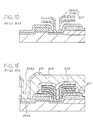
- a field oxide film 202 is formed on the surface of a p-type silicon substrate 201, and an MOS transistor consisting of a gate electrodd 203 which serves for both of a gate oxide film 202a and a word line, an n-type node diffused layer 204a, and an n-type bit diffused layer 204b is formed.
- a first interlayer insulating film 205 is deposited allover the surface. At least the surface of the interlayer insulating film 205 is formed of a silicon nitride film.
- a silicon oxide film 227, a first n-type polycrystalline silicon film 213, and a silicon oxide film 228 are formed sequentially (FIG. 1A).
- a photoresist film 218 which has an opening at the position where a node contact hole is to be created is formed, and a node contact hole 206a which reaches the node diffused layer 204a is opened by etching sequentially the silicon oxide film 228, the polycrystalline silicon film 212, the silicon oxide film 227, and the interlayer insulating film 205.
- the silicon oxide film 228, the polycrystalline silicon film 213, and the silicon oxide film 227 become a silicon oxide film 228a, a polycrystalline silicon film 213a, and a silicon oxide film 227a, respectively (FIG. 1B).
- the photoresist film 218 is removed, and a second n-type polycrystalline silicon film is formed allover the surface.
- a photoresist film 219 is formed in the region where a node electrode is to be formed, the second n-type polycrystalline silicon film, the silicon oxide film 228a, the polycrystalline silicon film 213a and the silicon oxide film 227a are sequentially etched by an anisotropic etching such as an RIE that uses the photoresist film 219 as the mask.
- the second n-type polycrystalline silicon film, the silicon oxide film 228a, the polycrystalline silicon film 213a, and the silicon oxide film 227a are converted to a polycrystalline silicon film 223a, a silicon oxide film 228b, a polycrystalline silicon film 213b, and a silicon oxide film 227b, respectively (FIG. 1C).
- the silicon oxide film 228b sandwiched by the polycrystalline silicon film 223a and the polycrystalline silicon film 213b, and the silicon oxide film 227b sandwiched by the polycrystalline silicon film 213b and the interlayer insulating film 205 are removed by a wet etching which uses hydrofluoric acid.
- a node electrode 217 of fin structure constituted of an n-type polycrystalline silicon film 223a and an n-type polycrystalline silicon film 2I3b is formed (FIG. 1D).
- a capacitor insulating film 207 is deposited allover the surface.
- a third n-type polycrystalline silicon film is formed allover the surface, and a cell plate electrode 208 is formed by etching the third n-type polycrystalline silicon film.
- a stacked type capacitor is formed by removing the capacitor insulating film 207 by etching, using the cell plate electrode 208 as the mask.
- a second interlayer insulating film 209 is deposited allover the surface, and a bit contact hole 208 is opened by sequentially etching the interlayer insulating films 209 and 205 above the bit diffused layer 204b.
- a bit line 210 is formed, completing a DRAM (FIG. 1E).
- the node electrode 217 of fin structure as shown in FIG. 1D has a sufficiently large surface area.
- the mechanical strength of the node electrode 217 is deteriorated, making the process such as washing extremely difficult.
- FIGs. 2A to 2E are schematic sectional views arranged in the order of the processes to describe the manufacturing method of the first embodiment of the present invention
- an active region and an element isolation region are partitioned by forming a field oxide film 102 on the surface of a p-type silicon substrate 101.
- a gate electrode 103 which is served also as a word line is formed.
- An n-type node diffused layer 104a and a bit diffused layer 104b are formed on the surface of the active region by using the gate electrode 103 on the active region as the mask, completing a MOS transistor of a DRAM.
- a first interlayer insulating film 105 consisting of a silicon oxide film with thickness of, for example, about 300 nm is formed allover the surface.
- the interlayer insulating film 105 needs not have at least its surface be constituted of a silicon nitride film, as is the case in the conventional device.
- the structure shown in FIG. 2A is obtained by opening a node contact hole 106a by etching the interlayer insulating film 105 on the node diffused layer 104a.
- a undoped polycrystalline silicon film 111 with thickness of, for example, about 150 nm is deposited by thermal decomposition of silane (SiH4) within the temperature range of 500 to 600°C in an LPCVD apparatus.
- an oxygen-rich undoped polycrystalline silicon film 112 is formed by exposing the sample to an argon atmosphere containing 0.2 to 5% of oxygen (O2) in the same apparatus.
- an undoped polycrystalline silicon film 121, an oxygen-rich undoped polycrystalline silicon film 122, a undoped polycrystalline silicon film 131, and an oxygen-rich undoped polycrystalline silicon film 132 are formed sequentially to form a stacked polycrystalline silicon film, obtaining the structure as shown in FIG. 2B.
- the flow rate of silane and argon diluting oxygen are changed periodically as shown, for example, in FIG. 3.
- the film thicknesses of the oxygen-rich undoped polycrystalline silicon films 112, 122, and 132 formed on the surfaces of the undoped polycrystalline silicon films 111, 121, and 131, respectively, are determined by the temperature, pressure, and oxygen partial pressure within the LPCVD apparatus, duration of the operation, and the like, but they are considered to be the thicknesses corresponding to silicon layers with one to several atomic layers. At this time, it is considered that the bonding between oxygen and silicon is not forming the complete structure of silicon dioxide (SiO2).
- the sample is taken out of the LPCVD apparatus and is subjected to diffusion by phosphoryl trichloride (POCl3) bubbling at 800 to 850°C to convert the undoped polycrystalline silicon films 111, 121, and 131 and the oxygen-rich undoped polycrystalline silicon films 112, 122, and 132 to n-type semiconductor films.
- POCl3 phosphoryl trichloride
- the thickness of the oxygen-rich n-type polycrystalline silicon film is 5 to 200 nm, and the sheet resistance of the film is 200 to 1000 ⁇ / ⁇ or so.
- the depth profile of the oxygen concentration is as shown in FIG. 4.
- This result represents a measurement by secondary ion mass spectrometry (SIMS).
- SIMS secondary ion mass spectrometry
- the oxygen concentration has three peaks; a first peak on the surface, a second peak at a depth of about 150 nm, and a third peak at a depth of about 300 nm.
- the second and the third peaks have a considerable spectral width, and the maximum oxygen concentrations at these peaks are about one order of magnitude smaller than the oxygen concentration of a silicon oxide film.
- the first peak is in the state of superposition of a region of extremely high oxygen concentration (about 5 x 10²¹ atoms/cm3 which is comparable to the oxygen concentration of the interlayer insulating film) in a very narrow range, and a region which is the same order as those of the second and the third peaks.
- the region of the first peak with extremely high oxygen concentration corresponds to the region of natural oxide formed on the surface of the stacked film.
- a photoresist film 119 is formed in the region reserved for a node electrode, and an anisotropic etching is applied to the stacked film consisting of the n-type polycrystalline silicon.
- a stacked film consisting of an oxygen-rich n-type polycrystalline silicon film 134b, an n-type polycrystalline silicon film 133b, an oxygen-rich n-type polycrystalline silicon film 124b, an n-type polycrystalline silicon film 123b, an oxygen-rich n-type polycrystalline silicon film 114b, and an n-type polycrystalline silicon film 113b, as shown in FIG. 2C.
- the side faces of the stacked film is approximately flat.
- the anisotropic etching is an RIE that uses dichlorodifluoromethane (CCl2F2) of about 40 sccm as the etchant gas, carried out under a pressure of about 200 m Torr and an RF power of about 300 W.
- Cl2F2 dichlorodifluoromethane
- an isotropic etching is applied without removal of the photoresist film 119 to the exposed surfaces of the stacked film, by using sulfur hexafluoride (SF6) as the etchant gas.
- SF6 sulfur hexafluoride
- the oxygen-rich n-type polycrystalline silicon film 134b, the n-type polycrystalline silicon film 133b, the oxygen-rich n-type polycrystalline silicon film 124b, the n-type polycrystalline silicon film 123b, the oxygen-rich n-type polycrystalline silicon film 114b, and the n-type polycrystalline silicon film 113b are converted respectively to an oxygen-rich n-type polycrystalline silicon film 134c, an n-type polycrystalline silicon film 133c, an oxygen-rich n-type polycrystalline silicon film 124c, an n-type polycrystalline silicon film 123c, an oxygen-rich n-type polycrystalline silicon film 114c, and an n-type polycrystalline silicon film 113c, as shown in FIG. 2D,
- the isotropic etching employed here is carried out, for example, using sulfur hexafluoride of 60 sccm as the etchant gas and helium (He) of 100 sccm as the carrier gas, under a pressure of 400 m Torr and an RF power of 400 W.
- the indentations in this case is about 0.1 to 0.3 ⁇ m.
- the increase in the surface area of the node electrode 117a due to individual indentation is small, for example, even if the increase in the surface area due to a single indentation is about 6%, the surface area of the node electrode can be increased by increasing the layer number of the oxygen-rich polycrystalline films, as shown in FIG. 5.
- the layer number of the n-type polycrystalline silicon films that do not contain oxygen (or are oxygen-poor) is three, and the thickness of each film is about 150 nm, so that the increase in the surface area of the node electrode is about 18%.
- the increase in the surface area of the node electrode can be made about 60%.
- a capacitor insulating film 107 and a cell plate electrode 108 are formed, completing a stacked capacitor.
- a second interlayer insulating film 109 is deposited allover the surface, and a bit contact hole 106b is opened by sequentially etching the interlayer insulating films 109 and 105 on the bit diffused layer 104b.
- a bit line 110 is formed to complete a DRAM which is equipped with the node electrode 117a of the first embodiment as shown in FIG. 2E.
- the present embodiment makes it possible to obtain the fin structure in smaller number of steps of one time of photolithography process (and two times of etching process) compared with the conventional manufacturing method. Furthermore, the depth of the indentation of the fins is about 0.3 ⁇ m at the most so that the mechanical strength at the stage of formation of the node electrode can be secured. Moreover, as described in the above, the number of indentations on the side faces of the node electrode can readily be increased, so that it is easy to obtain a capacitor having large capacitance even if the occupancy area of the stacked capacitor has to be decreased.
- FIGs. 6A and 6B are schematic sectional views of the principal processes to describe the manufacturing method of the second embodiment of the semiconductor memory device of the present invention, it can be seen that the formation of the present embodiment is the same as that of the first embodiment up to the process shown in FIG. 2A.
- an oxygen-rich n-type polycrystalline silicon film 114 is formed on the surface of the polycrystalline silicon film 113 by exposing the sample to an argon atmosphere containing 0.2 to 5% of oxygen (O2) within the same apparatus.
- an n-type polycrystalline silicon film 123, an oxyen-rich n-type polycrystalline silicon film 124, an n-type polycrystalline silicon film 133, and an oxygen-rich n-type polycrystalline silicon film 134 are formed sequentially to form a stacked polycrystalline silicon film, obtaining the structure as shown in FIG. 6A.
- the oxygen-rich n-typpe polycrystalline silicon film 134, the n-type polycrystalline silicon film 133, the oxygen-rich n-type polycrystalline silicon film 124, the n-type polycrystalline silicon film 123, the oxygen-rich n-type polycrystalline silicon film 114, and the n-type polycrystalline silicon film 113 are respectively converted to an oxygen-rich n-type polycrystalline silicon film 134a, an n-type polycrystalline silicon film 133a, an oxygen-rich n-type polycrystalline silicon film 124a, an n-type polycrystalline silicon film 123a, an oxygen-rich n-type polycrystalline silicon film 114a, and an n-type polycrystalline silicon film 113a, as shown in FIG.
- the purpose of the heat treatment is to disperse oxygen in, for example, the oxygen-rich n-type polycrystalline silicon film 114, and as a result, the thickness of the oxygen-rich n-type polycrystalline silicon film 114a is increased than the thickness of the oxygen-rich n-type polycrystalline silicon film 114.
- a node electrode of the present embodiment is completed through processes similar to those shown in FIGs. 2C and 2D of the first embodiment. Further, a DRAM equipped with the node electrode of the present embodiment is completed by the same manufacturing method as shown in FIG. 2E of the first embodiment.
- a stacked film is formed consisting of polycrystalline silicon films which are n-type from the beginning.
- the growth rate of the n-type polycrystalline silicon film by the above-mentioned method is smaller than the growth rate of the undoped polycrystalline silicon film of the first embodiment.
- the method of the present embodiment it becomes possible to form with high accuracy an n-type polycrystalline silicon film with small thickness.
- the thickness of the oxygen-rich n-type polycrystalline silicon film 114a depends on the conditions of the heat treatment. Therefore, the thickness of the n-type polycrystalline silicon film 113a and the oxygen-rich n-type polycrystalline silicon film 114a, for example, can further be reduced compared with the first embodiment.
- the present embodiment makes it possible to further increase the surface area of the side faces of the node electrode than in the first embodiment.
- the stacked film consisting of the polycrystalline silicon films in the first and the second embodiments were made by an LPCVD method.
- FIGs. 7A to 7D which show schematic sectional views of the principal processes to describe the third embodiment of the present invention and the manufacturing method thereof, the present embodiment is formed in the same way as in the first embodiment up to the process as shown in FIG. 2A.
- a tungsten silicide film 115 with thickness of, for example, about 50 nm is formed on the polycrystalline silicon film 111 by the reaction of tungsten hexafluoride (WF6) akd silane (the so-called silane reduction method) within the same apparatus. Since the growth rate of the tungsteh silicide film is a fraction of the growth rate of the undoped polycrystalline silicon film 111, the tungsten silicide film can be formed with high accuracy in the thickness.
- an undoped polycrystalline silicon film 121 with thickness of about 100 nm, a tungsten silicide film 125 with thickness of about 50 nm, an undoped polycrystalline silicon film 131 with thickness of about 100 nm, and a tungsten silicide film 136 with thickness of about 100 nm are formed, obtaining the structure as shown in FIG. 7A.
- the tungsten silicide film 136 is set to have a greater thickness than the thicknesses of other tungsten silicide films 115 and 125.
- the lowermost film be a polycrystalline silicon film. This is for obtaining satisfactory close contact and ohmic contact property between the node diffused layer 104a and the node electrode yet to be formed in the node contact hole 106a.
- a photoresist film 119a is formed in the region for forming the node electrode.
- a stacked film consisting of a tungsten silicide film 136a, an undoped polycrystalline silicon film 131a, a tungsten silicide film 125a, an undoped polycrystalline silicon film 121a, a tungsten silicide film 115a, and an undoped polycrystalline silicon film 111a is formed at the position for forming the node electrode by means of an anisotropic etching, as shown in FIG. 7B.
- This anisotropic etching is an RIE which uses tetrafluoromethane (CF4).
- the etching conditions are: a flow rate of 50 sccm of tetrafluoromethane, a pressure of 100 m Torr, and an RF power of 300 W.
- the interlayer insulating film 105 cannot act as a stopper for the etching because of the high etching rate for the silicon oxide film. For this reason, the etching of the lowermost undoped polycrystalline film 111 requires a through attention.
- the photoresist film 119 is removed to give diffusion of phosphorus.
- the undoped polycrystalline silicon films 131a, 121a, and 111a are converted to the respectively n-type polycrystalline silicon films 133b, 123b, and 113b as shown in FIG. 7C. That this diffusion of phosphorus is possible is due to the fact that the difission coefficient in the polycrystalline silicon film is greater than that in single crystal silicon by about one order of magnitude.
- the stacked film sonsisting of the rungsten silicide film 136a, the n-type polycrystaline silicon film 133b, the tungsten silicide film 125a, the n-type polycrystalline silicon film 123b, the tungsten silicide film 115a, and the n-type polycrystalline silicon film 113b is converted to a stacked film consisting of a tungsten silicide film 136b, an n-type polycrystalline silicide film 133c, a tungsten silicide film 125b, an n-type polycrystalline silicon film 123c, a tungsten silicide film 115b, and an n-type polycrystalline silicon film 113c.
- SF6 sulfur hexafluoride
- a node electrode 117b is constituted of this stacked film. Since the etching rate of the n-type polycrystalline silicon film is sufficiently large (high selection ratio) compared with the etching rate of the tungsten silicide film, there are formed indentations due to the n-type polycrystalline silicon films on the side faces of the node electrode 117b. In order to form these indentations in an effective manner it is preferable that the topmost layer is a tungsten silicide film rather than a polycrystalline silicon film. Since the thickness of the tungsten silicide film 136a in the uppermost layer is reduced during the etching, it is preferable that this layer is set to have a larger thickness than other tungsten silicide film, as mentioned in the above.
- the isotropic etching by an etchant gas containing sulfur hexafluoride (SF6) will be described in more detail.
- a dry etching for example, which uses an etchant gas of the mixture of sulfur hexafluoride of 50 sccm and chlorine (Cl2) gas of 50 sccm and carried out a pressure of 100 to 150 m Torr and an RF power of 200 to 300 W, the etching rates of the tungsten silicide film and the n-type polycrystalline silicon film are 70 to 90 nm/min and 600 to 700 nm/min, respectively.
- sulfur hexafluoride alone, or mix gas of sulfur hexafluoride and hydrogen bromide (HBr) may also be used as the etchant gas. It is preferable that this isotropic etching is applied after conversion of the polycrystalline silicon films to the n-type films. In the undoped polycrystalline silicon film, the selectivity ratio of the etching rate of this film with respect to that of the tungsten silicide film is reduced.
- a DRAM including the node electrode according to the present embodiment is completed by forming a capacitor insulating film, a cell plate electrode, a second interlayer insulating film, a bit contact hole, and a bit line in the same manner as in the first embodiment.
- a silicon oxide film obtained by thermal oxidation as the capacitor insulating film.
- the etching rate of the n-type polycrystalline silicon film is sufficiently larger than the etching rate of the tungsten silicide film, so that the indentations formed on the side faces of the node electrode in the present embodiment have greater depth than in the indentations of the first and the second embodiments. Moreover, the surface area of the node electrode becomes larger than those in the first and the second embodiments.
- the n-type polycrystalline silicon film was used as the first conductor film and the tungsten silicide film was used as the second conductor film.
- a high melting point metal such as a molybdenum silicide film or a titanium silicide film
- FIGs. 8A to 8C which. are schematic sectional views of the principal processes to describe the manufacturing method of the fourth embodiment of the semiconductor memory device of the present invention, the present embodiment is formed in the same way as in the first embodiment up to the process shown in FIG. 2A.
- a tungsten silicide film 115 with thickness of, for example, about 75 nm is formed on the polycrystalline silicon film 113 ny the reaction within the same apparatus of tungsten hexafluoride (WF6) and silane (the so-called silane reduction method).
- the growth rates of the tungsten silicide film and the n-type polycrystalline silicon film are approximately the same, being a fraction of the growth rate of the undoped polycrystalline silicon film 111 in the third embodiment, so that the tungsten silicide film and the n-type polycrystalline silicon film can be formed with high accuracy of the thickness.
- an n-type polycrystalline film 123 with thickness of about 75 nm, a tungsten silicide film 125 with thickness of about 75 nm, an n-type polycrystalline silicon film 133, and a tungsten silicide film 135 with thickness of about 75 nm are formed, obtaining the structure as shown in FIG. 8A.
- a photoresist film 119b is formed in the region where a node electrode is to be formed.
- a stacked film consisting of a tungsten silicide film 135a, an n-type polycrystalline silicon film 133b, a tungsten silicide film 125a, an n-type polycrystalline silicon film 123b, a tungsten silicide film 115a, and an n-type polycrystalline silicon film 113b is formed at the position where the node electrode is to be formed by an anisotropic etching as shown in FIG. 8B. This anisotropic etching is carried out under the same conditions as in the third embodiment.
- a node electrode 117b of the present embodiment formed by a stacked film consisting of a tungsten silicide film 135b, an n-type polycrystalllne silicon film 133c, a tungsten silicide film 125b, an n-type polycrystalline silicon film 123c, a tungsten silicide film 115b, and an n-type polycrystalline silicon film 113c, as shown in FIG. 8C.
- a DRAM having the node electrode of the present embodiment is obtained by forming a capacitor insulating film, a cell plate electrode, a second interlayer insulating film, a bit contact hole, and a bit line in the same way as in the first embodiment.
- the present embodiment is superior to the third embodiment is the controllability of the formation of the tungsten silicide film and the n-type polycrystalline silicon film. Therefore, it becomes easier to increase the number of identations in the side faces of the node electrode by setting the thickness of each film thinner, making it easy to increase the surface area of the node electrode compared with the third embodiment.
- the n-type polycrystalline silicon film is used as the first conductor film
- the oxygen-rich polycrystalline silicon film or the tungsten silicide film is used as the second conductor film
- dry etching using an etchant gas containing at least sulfur hexafluoride (SF6) is employed as the isotropic etching, but the present invention is by no means limited to the above-mentioned combination.
- SF6 sulfur hexafluoride
- One of the conditions in the selection of the materials for the first and the second conductor films is that the selectivity ratio of the etching rates of the first and the second conductor films for the isotropic etching has a sufficiently large value.
Landscapes
- Engineering & Computer Science (AREA)
- Manufacturing & Machinery (AREA)
- Semiconductor Memories (AREA)
Applications Claiming Priority (4)
| Application Number | Priority Date | Filing Date | Title |
|---|---|---|---|
| JP291538/90 | 1990-10-29 | ||
| JP29153890 | 1990-10-29 | ||
| JP03041474A JP3104262B2 (ja) | 1991-03-07 | 1991-03-07 | 半導体装置およびその製造方法 |
| JP41474/91 | 1991-03-07 |
Publications (2)
| Publication Number | Publication Date |
|---|---|
| EP0484088A1 true EP0484088A1 (de) | 1992-05-06 |
| EP0484088B1 EP0484088B1 (de) | 1996-05-08 |
Family
ID=26381099
Family Applications (1)
| Application Number | Title | Priority Date | Filing Date |
|---|---|---|---|
| EP91309956A Expired - Lifetime EP0484088B1 (de) | 1990-10-29 | 1991-10-29 | DRAM Zelle mit Stapelkondensator |
Country Status (4)
| Country | Link |
|---|---|
| US (2) | US5504704A (de) |
| EP (1) | EP0484088B1 (de) |
| KR (1) | KR960016837B1 (de) |
| DE (1) | DE69119354T2 (de) |
Cited By (2)
| Publication number | Priority date | Publication date | Assignee | Title |
|---|---|---|---|---|
| DE4238081A1 (en) * | 1992-01-21 | 1993-07-22 | Mitsubishi Electric Corp | Stacked capacitor for semiconductor DRAM storage cell - has step in upper surface of lower electrode, with field insulation film formed on silicon substrate, e.g. by LOCOS process |
| EP0756326A1 (de) * | 1995-07-24 | 1997-01-29 | Siemens Aktiengesellschaft | Kondensator in einer Halbleiteranordnung und Verfahren zu seiner Herstellung |
Families Citing this family (30)
| Publication number | Priority date | Publication date | Assignee | Title |
|---|---|---|---|---|
| JP2542706B2 (ja) * | 1989-10-05 | 1996-10-09 | 株式会社東芝 | ダイナミックram |
| JPH0621018A (ja) * | 1992-06-29 | 1994-01-28 | Sony Corp | ドライエッチング方法 |
| KR960003771B1 (ko) * | 1992-08-08 | 1996-03-22 | 삼성전자주식회사 | 반도체 메모리장치 |
| US5436186A (en) * | 1994-04-22 | 1995-07-25 | United Microelectronics Corporation | Process for fabricating a stacked capacitor |
| KR0136533B1 (ko) * | 1994-06-09 | 1998-09-15 | 문정환 | 불휘발성 반도체 메모리 소자 및 그의 제조방법 |
| JPH0831174A (ja) * | 1994-07-18 | 1996-02-02 | Fujitsu Ltd | 半導体記憶装置 |
| KR960006030A (ko) * | 1994-07-18 | 1996-02-23 | 김주용 | 반도체소자의 캐패시터 제조방법 |
| US5538592A (en) * | 1994-07-22 | 1996-07-23 | International Business Machines Corporation | Non-random sub-lithography vertical stack capacitor |
| US5564180A (en) * | 1994-11-14 | 1996-10-15 | United Microelectronics Corp. | Method of fabricating DRAM cell capacitor |
| KR0155785B1 (ko) * | 1994-12-15 | 1998-10-15 | 김광호 | 핀형 커패시터 및 그 제조방법 |
| US5672535A (en) * | 1995-05-31 | 1997-09-30 | Alliance Semiconductor Corporation | Method of fabricating DRAM cell with self-aligned contact |
| US5701264A (en) * | 1995-12-13 | 1997-12-23 | Alliance Semiconductor Corporation | Dynamic random access memory cell having increased capacitance |
| US5792708A (en) * | 1996-03-06 | 1998-08-11 | Chartered Semiconductor Manufacturing Pte Ltd. | Method for forming residue free patterned polysilicon layers upon high step height integrated circuit substrates |
| US5591664A (en) * | 1996-03-20 | 1997-01-07 | Taiwan Semiconductor Manufacturing Company Ltd. | Method of increasing the capacitance area in DRAM stacked capacitors using a simplified process |
| US5994730A (en) | 1996-11-21 | 1999-11-30 | Alliance Semiconductor Corporation | DRAM cell having storage capacitor contact self-aligned to bit lines and word lines |
| TW311258B (en) * | 1997-01-24 | 1997-07-21 | United Microelectronics Corp | Manufacturing method of stack capacitor of dynamic random access memory |
| JP3373134B2 (ja) * | 1997-06-13 | 2003-02-04 | 沖電気工業株式会社 | 半導体装置の製造方法 |
| US5970358A (en) * | 1997-06-30 | 1999-10-19 | Micron Technology, Inc. | Method for forming a capacitor wherein the first capacitor plate includes electrically coupled conductive layers separated by an intervening insulative layer |
| US5903493A (en) * | 1997-09-17 | 1999-05-11 | Lucent Technologies Inc. | Metal to metal capacitor apparatus and method for making |
| US6329703B1 (en) * | 1998-02-25 | 2001-12-11 | Infineon Technologies Ag | Contact between a monocrystalline silicon region and a polycrystalline silicon structure and method for producing such a contact |
| US6210813B1 (en) * | 1998-09-02 | 2001-04-03 | Micron Technology, Inc. | Forming metal silicide resistant to subsequent thermal processing |
| KR100311498B1 (ko) | 1999-01-12 | 2001-11-02 | 김영환 | 반도체 소자의 이중 게이트 형성방법 |
| KR100313510B1 (ko) | 1999-04-02 | 2001-11-07 | 김영환 | 반도체 소자의 제조방법 |
| AU2002306436A1 (en) | 2001-02-12 | 2002-10-15 | Asm America, Inc. | Improved process for deposition of semiconductor films |
| US7320131B1 (en) * | 2001-06-06 | 2008-01-15 | Cisco Technology, Inc. | Methods and apparatus for selecting a server to process a request |
| US7186630B2 (en) * | 2002-08-14 | 2007-03-06 | Asm America, Inc. | Deposition of amorphous silicon-containing films |
| US6746877B1 (en) * | 2003-01-07 | 2004-06-08 | Infineon Ag | Encapsulation of ferroelectric capacitors |
| US7005160B2 (en) * | 2003-04-24 | 2006-02-28 | Asm America, Inc. | Methods for depositing polycrystalline films with engineered grain structures |
| US8629063B2 (en) * | 2011-06-08 | 2014-01-14 | International Business Machines Corporation | Forming features on a substrate having varying feature densities |
| US9048212B2 (en) * | 2012-05-15 | 2015-06-02 | Taiwan Semiconductor Manufacturing Company, Ltd. | Semiconductor devices, methods of manufacture thereof, and methods of manufacturing capacitors |
Citations (1)
| Publication number | Priority date | Publication date | Assignee | Title |
|---|---|---|---|---|
| EP0295709A2 (de) * | 1987-06-17 | 1988-12-21 | Fujitsu Limited | Dynamische Speicherzelle mit wahlfreiem Zugriff und Verfahren zu ihrer Herstellung |
Family Cites Families (5)
| Publication number | Priority date | Publication date | Assignee | Title |
|---|---|---|---|---|
| JPH0682783B2 (ja) * | 1985-03-29 | 1994-10-19 | 三菱電機株式会社 | 容量およびその製造方法 |
| US4901043A (en) * | 1987-07-02 | 1990-02-13 | Andrew F. Tresness | Compact filter having a multi-compartment housing |
| JPS6420050A (en) * | 1987-07-14 | 1989-01-24 | Maruka Kk | Production of boneless fish |
| JPH01120050A (ja) * | 1987-11-02 | 1989-05-12 | Hitachi Ltd | 半導体記憶装置 |
| JPH0210762A (ja) * | 1988-06-28 | 1990-01-16 | Mitsubishi Electric Corp | キャパシタ |
-
1991
- 1991-10-29 EP EP91309956A patent/EP0484088B1/de not_active Expired - Lifetime
- 1991-10-29 KR KR91019264A patent/KR960016837B1/ko not_active Expired - Fee Related
- 1991-10-29 DE DE69119354T patent/DE69119354T2/de not_active Expired - Fee Related
- 1991-10-29 US US07/784,269 patent/US5504704A/en not_active Expired - Lifetime
-
1994
- 1994-09-01 US US08/299,885 patent/US5416037A/en not_active Expired - Lifetime
Patent Citations (1)
| Publication number | Priority date | Publication date | Assignee | Title |
|---|---|---|---|---|
| EP0295709A2 (de) * | 1987-06-17 | 1988-12-21 | Fujitsu Limited | Dynamische Speicherzelle mit wahlfreiem Zugriff und Verfahren zu ihrer Herstellung |
Non-Patent Citations (2)
| Title |
|---|
| PATENT ABSTRACTS OF JAPAN vol. 13, no. 359 (E-804)[3707] 10 August 1989 & JP-A-1 120 050 ( HITACHI LTD. ) 12 May 1989 * |
| PATENT ABSTRACTS OF JAPAN vol. 14, no. 151 (E-906)[4094] 22 March 1990 & JP-A-2 010 762 ( MITSUBUSHI ELECTRIC CORP. ) 16 January 1990 * |
Cited By (3)
| Publication number | Priority date | Publication date | Assignee | Title |
|---|---|---|---|---|
| DE4238081A1 (en) * | 1992-01-21 | 1993-07-22 | Mitsubishi Electric Corp | Stacked capacitor for semiconductor DRAM storage cell - has step in upper surface of lower electrode, with field insulation film formed on silicon substrate, e.g. by LOCOS process |
| EP0756326A1 (de) * | 1995-07-24 | 1997-01-29 | Siemens Aktiengesellschaft | Kondensator in einer Halbleiteranordnung und Verfahren zu seiner Herstellung |
| US5989972A (en) * | 1995-07-24 | 1999-11-23 | Siemens Aktiengesellschaft | Capacitor in a semiconductor configuration and process for its production |
Also Published As
| Publication number | Publication date |
|---|---|
| EP0484088B1 (de) | 1996-05-08 |
| DE69119354T2 (de) | 1996-09-19 |
| KR960016837B1 (en) | 1996-12-21 |
| DE69119354D1 (de) | 1996-06-13 |
| US5504704A (en) | 1996-04-02 |
| US5416037A (en) | 1995-05-16 |
Similar Documents
| Publication | Publication Date | Title |
|---|---|---|
| US5416037A (en) | Method of making a semiconductor memory device | |
| US4742018A (en) | Process for producing memory cell having stacked capacitor | |
| US5612558A (en) | Hemispherical grained silicon on refractory metal nitride | |
| US5696395A (en) | Dynamic random access memory with fin-type stacked capacitor | |
| JP3123073B2 (ja) | 半導体記憶装置の製造方法 | |
| US5436188A (en) | Dram cell process having elk horn shaped capacitor | |
| US7214981B2 (en) | Semiconductor devices having double-sided hemispherical silicon grain electrodes | |
| KR960012254B1 (ko) | 반도체 장치 및 그 제조 방법 | |
| US7432152B2 (en) | Methods of forming HSG layers and devices | |
| JP2817645B2 (ja) | 半導体装置の製造方法 | |
| DE19947053C1 (de) | Grabenkondensator zu Ladungsspeicherung und Verfahren zu seiner Herstellung | |
| JP4748887B2 (ja) | 半導体メモリの製造方法 | |
| US6204119B1 (en) | Manufacturing method for a capacitor in an integrated memory circuit | |
| JP2826324B2 (ja) | 半導体素子の製造方法 | |
| JPH08306876A (ja) | 半導体装置の製造方法 | |
| JP2621609B2 (ja) | 電荷蓄積容量を備えた半導体装置及びその製造方法 | |
| EP0428732A1 (de) | Verfahren zur herstellung von halbleiteranordnungen | |
| JP3067329B2 (ja) | 半導体記憶装置およびその製造方法 | |
| JPH0734451B2 (ja) | 半導体装置の製造方法 | |
| JPH0567751A (ja) | 半導体装置の製造方法 | |
| JP3196373B2 (ja) | 半導体装置の製造方法 | |
| KR100384793B1 (ko) | 커패시터의 제조방법 | |
| JPH05299579A (ja) | 半導体装置の製造方法 | |
| JPH05167036A (ja) | 半導体メモリの製造方法 | |
| JPH08335675A (ja) | 半導体装置の製造方法 |
Legal Events
| Date | Code | Title | Description |
|---|---|---|---|
| PUAI | Public reference made under article 153(3) epc to a published international application that has entered the european phase |
Free format text: ORIGINAL CODE: 0009012 |
|
| 17P | Request for examination filed |
Effective date: 19911119 |
|
| AK | Designated contracting states |
Kind code of ref document: A1 Designated state(s): DE FR GB |
|
| 17Q | First examination report despatched |
Effective date: 19940315 |
|
| GRAH | Despatch of communication of intention to grant a patent |
Free format text: ORIGINAL CODE: EPIDOS IGRA |
|
| GRAA | (expected) grant |
Free format text: ORIGINAL CODE: 0009210 |
|
| AK | Designated contracting states |
Kind code of ref document: B1 Designated state(s): DE FR GB |
|
| REF | Corresponds to: |
Ref document number: 69119354 Country of ref document: DE Date of ref document: 19960613 |
|
| ET | Fr: translation filed | ||
| PLBE | No opposition filed within time limit |
Free format text: ORIGINAL CODE: 0009261 |
|
| STAA | Information on the status of an ep patent application or granted ep patent |
Free format text: STATUS: NO OPPOSITION FILED WITHIN TIME LIMIT |
|
| 26N | No opposition filed | ||
| REG | Reference to a national code |
Ref country code: GB Ref legal event code: IF02 |
|
| REG | Reference to a national code |
Ref country code: GB Ref legal event code: 732E |
|
| REG | Reference to a national code |
Ref country code: FR Ref legal event code: TQ |
|
| REG | Reference to a national code |
Ref country code: GB Ref legal event code: 732E |
|
| REG | Reference to a national code |
Ref country code: FR Ref legal event code: TP Ref country code: FR Ref legal event code: TQ |
|
| PGFP | Annual fee paid to national office [announced via postgrant information from national office to epo] |
Ref country code: GB Payment date: 20061025 Year of fee payment: 16 |
|
| PGFP | Annual fee paid to national office [announced via postgrant information from national office to epo] |
Ref country code: DE Payment date: 20061026 Year of fee payment: 16 |
|
| GBPC | Gb: european patent ceased through non-payment of renewal fee |
Effective date: 20071029 |
|
| PG25 | Lapsed in a contracting state [announced via postgrant information from national office to epo] |
Ref country code: DE Free format text: LAPSE BECAUSE OF NON-PAYMENT OF DUE FEES Effective date: 20080501 |
|
| REG | Reference to a national code |
Ref country code: FR Ref legal event code: ST Effective date: 20080630 |
|
| PGFP | Annual fee paid to national office [announced via postgrant information from national office to epo] |
Ref country code: FR Payment date: 20061010 Year of fee payment: 16 |
|
| PG25 | Lapsed in a contracting state [announced via postgrant information from national office to epo] |
Ref country code: GB Free format text: LAPSE BECAUSE OF NON-PAYMENT OF DUE FEES Effective date: 20071029 |
|
| PG25 | Lapsed in a contracting state [announced via postgrant information from national office to epo] |
Ref country code: FR Free format text: LAPSE BECAUSE OF NON-PAYMENT OF DUE FEES Effective date: 20071031 |