EP0484558B1 - Hochfrequenzspule und verfahren zu ihrer herstellung - Google Patents
Hochfrequenzspule und verfahren zu ihrer herstellung Download PDFInfo
- Publication number
- EP0484558B1 EP0484558B1 EP91909800A EP91909800A EP0484558B1 EP 0484558 B1 EP0484558 B1 EP 0484558B1 EP 91909800 A EP91909800 A EP 91909800A EP 91909800 A EP91909800 A EP 91909800A EP 0484558 B1 EP0484558 B1 EP 0484558B1
- Authority
- EP
- European Patent Office
- Prior art keywords
- coil
- coil conductors
- high frequency
- insulating layer
- conductors
- Prior art date
- Legal status (The legal status is an assumption and is not a legal conclusion. Google has not performed a legal analysis and makes no representation as to the accuracy of the status listed.)
- Expired - Lifetime
Links
- 238000004519 manufacturing process Methods 0.000 title claims abstract description 11
- 239000004020 conductor Substances 0.000 claims abstract description 112
- 239000000758 substrate Substances 0.000 claims abstract description 29
- 229920003002 synthetic resin Polymers 0.000 claims description 9
- 239000000057 synthetic resin Substances 0.000 claims description 9
- 238000005530 etching Methods 0.000 claims description 8
- 239000011810 insulating material Substances 0.000 claims description 4
- 239000011248 coating agent Substances 0.000 claims description 3
- 238000000576 coating method Methods 0.000 claims description 3
- 229920005989 resin Polymers 0.000 claims 3
- 239000011347 resin Substances 0.000 claims 3
- 239000010410 layer Substances 0.000 description 35
- 239000010408 film Substances 0.000 description 19
- 238000000034 method Methods 0.000 description 14
- 238000004544 sputter deposition Methods 0.000 description 7
- 230000003247 decreasing effect Effects 0.000 description 4
- 239000010409 thin film Substances 0.000 description 3
- 239000000919 ceramic Substances 0.000 description 2
- 238000010586 diagram Methods 0.000 description 2
- 230000000694 effects Effects 0.000 description 2
- 239000011521 glass Substances 0.000 description 2
- 229920001721 polyimide Polymers 0.000 description 2
- 239000004677 Nylon Substances 0.000 description 1
- 239000004642 Polyimide Substances 0.000 description 1
- 239000000853 adhesive Substances 0.000 description 1
- 230000001070 adhesive effect Effects 0.000 description 1
- PNEYBMLMFCGWSK-UHFFFAOYSA-N aluminium oxide Inorganic materials [O-2].[O-2].[O-2].[Al+3].[Al+3] PNEYBMLMFCGWSK-UHFFFAOYSA-N 0.000 description 1
- 230000018109 developmental process Effects 0.000 description 1
- 230000009977 dual effect Effects 0.000 description 1
- 239000003822 epoxy resin Substances 0.000 description 1
- 238000001704 evaporation Methods 0.000 description 1
- 230000008020 evaporation Effects 0.000 description 1
- -1 for example Substances 0.000 description 1
- 238000007733 ion plating Methods 0.000 description 1
- 238000010030 laminating Methods 0.000 description 1
- 229920001778 nylon Polymers 0.000 description 1
- 238000005498 polishing Methods 0.000 description 1
- 229920006122 polyamide resin Polymers 0.000 description 1
- 229920000647 polyepoxide Polymers 0.000 description 1
- 239000009719 polyimide resin Substances 0.000 description 1
- 230000007261 regionalization Effects 0.000 description 1
- 238000007650 screen-printing Methods 0.000 description 1
- 239000002356 single layer Substances 0.000 description 1
- 238000007738 vacuum evaporation Methods 0.000 description 1
Images

Classifications
-
- H—ELECTRICITY
- H01—ELECTRIC ELEMENTS
- H01F—MAGNETS; INDUCTANCES; TRANSFORMERS; SELECTION OF MATERIALS FOR THEIR MAGNETIC PROPERTIES
- H01F41/00—Apparatus or processes specially adapted for manufacturing or assembling magnets, inductances or transformers; Apparatus or processes specially adapted for manufacturing materials characterised by their magnetic properties
- H01F41/02—Apparatus or processes specially adapted for manufacturing or assembling magnets, inductances or transformers; Apparatus or processes specially adapted for manufacturing materials characterised by their magnetic properties for manufacturing cores, coils, or magnets
- H01F41/04—Apparatus or processes specially adapted for manufacturing or assembling magnets, inductances or transformers; Apparatus or processes specially adapted for manufacturing materials characterised by their magnetic properties for manufacturing cores, coils, or magnets for manufacturing coils
- H01F41/041—Printed circuit coils
- H01F41/045—Trimming
-
- H—ELECTRICITY
- H01—ELECTRIC ELEMENTS
- H01F—MAGNETS; INDUCTANCES; TRANSFORMERS; SELECTION OF MATERIALS FOR THEIR MAGNETIC PROPERTIES
- H01F17/00—Fixed inductances of the signal type
- H01F17/0006—Printed inductances
-
- H—ELECTRICITY
- H01—ELECTRIC ELEMENTS
- H01F—MAGNETS; INDUCTANCES; TRANSFORMERS; SELECTION OF MATERIALS FOR THEIR MAGNETIC PROPERTIES
- H01F17/00—Fixed inductances of the signal type
- H01F17/0006—Printed inductances
- H01F2017/0066—Printed inductances with a magnetic layer
Definitions
- the present invention relates generally to a high frequency coil having a structure in which strip-shaped coil conductors are formed on the surface of an insulating substrate and a method of fabricating the same, and more particularly, to a high frequency coil whose Q can be increased without increasing the thickness and the line width of coil conductors and a method of fabricating the same.
- the high frequency coil used in a microwave circuit or the like has had the following structure. More specifically, the high frequency coil has a structure in which a coil conductor, for example, of a spiral type, is formed on the surface of an insulating substrate, an input electrode and an output electrode are respectively formed in side edge portions opposed to each other of the insulating substrate, and the input electrode and the output electrode are electrically connected to an outer end and an inner end of the above coil conductor, respectively.
- the above described high frequency coil is disclosed in, for example, British Patent Publication GB2,223,624A.
- a coil conductor is formed by a thin film forming technique such as sputtering or vacuum evaporation. Therefore, the high frequency coil has the disadvantage in that the electrical resistance of the coil conductor is increased because the thickness of the coil conductor is not made too large, resulting in decreased Q of the coil. Therefore, attempts have been conventionally made to lower the electrical resistance of the coil conductor by increasing the thickness and the line width of the coil conductor so as to increase Q of the coil.
- the conventional high frequency coil has the disadvantage in that if the line width of the coil conductor is increased, the substrate is increased in size by the amount of the increase, to make it impossible to meet the recent requirement of miniaturization of electronic components.
- the high frequency coil has the disadvantage in that there occurs a undesirable phenomenon referred to as under etching.
- the thickness of a coil conductor is increased by superimposing on the upper surface of one coil conductor another coil conductor.
- the line width of the coil conductor and the spacing between portions where the coil conductors are wound are very small, i.e., several tens of micrometers, therby to make it very difficult in the fabrication to further superimpose on one coil conductor another coil conductor having the same size with high precision.
- DE-U-88 01 879 discloses an inductor comprising an electrical insulating support member, two spiral-type conductors being mounted on the two opposing surfaces of the insulating support member, and two central contact elements as well as two external contact elements. By means of a through hole the two centre contact elements of the two spiral-type conductors are connected to each other, and the external contact members represent the external terminals for this inductor.
- GB-A-2 083 952 discloses a microcoil assembly comprising a spiral-patterned flat conductor 1 which is formed on both surfaces of an insulating substrate.
- the conductors on both surfaces of the substrate are arranged so that electric current can flow through the two spiral-patterned conductors in the same directions.
- the two conductors comprise inner ends which are connected to each other by a through hole, and outer ends which form the external lead terminals of the microcoil assembly.
- JP-A-2-123 706 discloses a high frequency coil comprising a substrate, one spiral-patterned conductor being positioned on one of the surfaces of said substrate, and two terminal electrodes. This document does not deal with the reduction of the resistance of an inductor comprising two coil conductors being positioned on opposite surfaces of a insulating substrate.
- an object of the present invention is to eliminate the above described disadvantages of the conventional high frequency coil and to provide a high frequency coil having a structure in which Q can be increased without increasing the thickness and the line width of coil conductors and a method of fabricating the same.
- the inventors of the present application have found that if a pluarlity of high frequency coils are electrically connected in parallel so as to decrease the conductor resistance of coil conductors, the conductor resistance can be decreasd but the inductance is similarly decreased so that Q of the coil cannot be improved.
- the inventors have found that the amount of the decrease in conductor resistance is larger than the amount of the decrease in inductance if a pair of coil conductors are formed such that the directions of currents flowing through the coil conductors are the same and so as to be opposed to each other with the insulating layer being interposed therebetween and have found that Q of the coil can be increased because the decrease in inductance can be restrained, thereby to make the present invention.
- a high frequency coil according to the present invention has a structure comprising at least one insulating layer, a pair of coil conductors formed on both major surfaces of the insulating layer so as to be opposed to each other with the above insulating layer being interposed therebetween, and an input electrode and an output electrode formed on the above insulating layer, in which one end of each of the above pair of coil conductors is electrically connected to the input electrode and the other end thereof is electrically connected to the output electrode such that the directions of currents flowing through the above coil conductors are the same.
- the high frequency coil according to the present invention includes one having the following multilayer structure in addition to the above described structure in which a pair of coil conductors is formed on both major surfaces of one insulating layer. More specifically, the present invention also includes a structure comprising a plurality of insulating layers, in which the insulating layers and pairs of coil conductors are alternately laminated such that the pair of coil conductors is arranged on both major surfaces of each of the insulating layers laminated.
- an insulating layer made of an insulating material having sufficient mechanical strength to support coil conductors for example, glass or ceramics is generally used as the above described insulating layer.
- the insulating layers may be made of a flexible insulating material provided that the lowermost insulating layer is made of such a rigid insulating material.
- the known thin film forming technique such as a sputtering process, an evaporation process, an ion plating process or a screen printing process can be utilized. That is, a method of forming the coil conductors is not particularly limited.
- a method of fabricating a high frequency coil comprises the steps of preparing an insulating layer, forming a conductor on the entire surface of the above insulating layer, etching the above conductor to form first and second coil conductors formed so as to be opposed to each other while being separated by the insulating layer and input and output electrodes on both major surfaces of the above insulating layer, coating both the entire major surfaces of the above insulating layer with photosensitive synthetic resin to form photosensitive synthetic resin films, disposing masks on portions, which face the above input and output electrodes and one end of each of the coil conductors, of the above photosensitive synthetic resin films to expose and develop the photosensitive synthetic resin films, removing portions other than the portions of the photosensitive synthetic resin films hardened by the exposure after the development to expose the input and output electrodes and to form a through hole in the portion facing the above one end of each of the coil conductors, and forming a conductor film on the above insulating layer to electrically connect the output electrode to the one end of each
- a pair of coil conductors is formed so as to be opposed to each other while being separated by an insulating layer, and the directions of currents flowing through the coil conductors are the same. Accordingly, the decrease in conductor resistance is made larger than the decrease in inductance. Consequently, inductance L is relatively increased, as compared with that of the conventional high frequency coil having decreased conductor resistance. In the high frequency coil according to the present invention, therefore, Q of the coil can be increased by the amount of the relative increase in the inductance L.
- Q of the coil can be increased without increasing the thickness and the line width of the coil conductors. Consequently, the increase in size of components of the high frequency coil can be avoided, and no undesired phenomena such as under etching occur at the time of the fabrication of the high frequency coil.
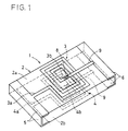
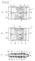
- Figs. 1 to 3 are diagrams for explaining a high frequency coil according to one embodiment of the present invention.
- a chip-type high frequency coil 1 is constructed by pattern formation of spiral-shaped first and second coil conductors 3 and 4 on both major surfaces 2a and 2b of an insulating substrate 2 made of glass or ceramics such as alumina.
- an input electrode 5 and an output electrode 6 are formed on both side surfaces of the above insulating substrate 2 in the longitudinal direction.
- Outer ends 3a and 4a of the above first and second coil conductors 3 and 4 are connected to the input electrode 5.
- the surfaces of the first and second coil conductors 3 and 4 excluding regions on the input and output electrodes 5 and 6 on both major surfaces of the above insulating substrate 2 are coated with insulating layers 7 made of polyimide or polyamide resin.
- Through holes 8 are formed in portions, which face inner ends 3b and 4b of the above first and second coil conductors 3 and 4, of the insulating layers 7.
- lead electrodes 9 are respectively formed on the upper surfaces of the above insulating layers 7, and one ends of the lead electrodes 9 are respectively connected to the inner ends 3b and 4b of the first and second coil conductors 3 and 4 through the above through holes 8 and the other ends thereof are respectively connected to the output electrode 6.
- first and second coil conductors 3 and 4 are so constructed that the directions of currents flowing through the first and second coil conductors 3 and 4 are the same.
- step (4) when the inner ends 3b and 4b of the coil conductors 3 and 4 are connected to the output electrode 6, a method of connecting the inner ends 3b and 4b and the output electrode 6 by wire bonding using an Au line and fastening them with nylon or adhesives of an epoxy resin system may be adopted.
- the first and second coil conductors 3 and 4 are formed on both the major surfaces 2a and 2b of the insulating substrate 2 so as to be opposed to each other with the substrate 2 being interposed therebetween, and the outer ends 3a and 4a of the coil conductors 3 and 4 are connected to the input electrode 5 and the inner ends 3b and 4b thereof are connected to the output electrode 6, thereby to make the directions of currents flowing through the coil conductors 3 and 4 the same. Accordingly, the conductor resistance can be reduced to approximately half, and Q of the coil can be improved because the decrease in inductance can be restrained.
- the value of Q is 30 (at 400 MHz) if the value of L is 18 nH.
- the value of Q is 35 (at 400 MHz) if the value of L is 10.5 nH, thereby to make it possible to improve Q by approximately 15 %.
- the first and second coil conductors 3 and 4 may be merely formed opposed to each other on both the major surfaces of the insulating substrate 2 by the thin film forming technique. Accordingly, the thickness and the line width of the coil conductors need not be increased unlike the conventional example. Consequently, the increase in size of components can be avoided, and there arise no problems such as under etching.
- the high frequency coil 1 according to the present embodiment is employed when the thickness and the line width of the coil conductors are made as large as possible and the conductor resistance is made smaller to improve Q, a larger effect is obtained.
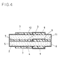
- the present invention may be applied to a multilayer coil constructed by forming one high frequency coil and then, forming an insulating layer in a portion excluding input and output electrodes and forming coil conductors on the upper surface of the insulating layer, or further repeatedly forming insulating layers and coil conductors. More specifically, as shown in Fig. 4, a multilayered high frequency coil may be constructed by further forming an insulating layer 11 and a third coil conductor 12 on a coil conductor 3 formed on the upper surface of one insulating substrate 2. Alternatively, a multilayered high frequency coil having more layers than those in the example as shown in Fig. 4 may be constructed by further laminating insulating layers and coil conductors.
Landscapes
- Engineering & Computer Science (AREA)
- Power Engineering (AREA)
- Manufacturing & Machinery (AREA)
- Microelectronics & Electronic Packaging (AREA)
- Coils Or Transformers For Communication (AREA)
Claims (7)
- Eine Hochfrequenzspule mit folgenden Merkmalen:
zumindest einer Isolationsschicht (2);
zumindest zwei Spulenleitern (3, 4), die auf zwei gegenüberliegenden Oberflächen der Isolationsschicht (2) gegenüberliegend zueinander angeordnet sind; und
einer Eingangselektrode (5) und einer Ausgangselektrode (6),
dadurch gekennzeichnet, daß
die Spulenleiter (3, 4) derart angeordnet sind, daß Ströme, die durch die zwei Spulenleiter (3, 4) fließen, die gleiche Richtung aufweisen; und
die Spulenleiter (3, 4) derart mit der Eingangselektrode (5) und der Ausgangselektrode (6) verbunden sind, daß die Spulenleiter (3, 4) elektrisch parallelgeschaltet sind. - Die Hochfrequenzspule gemäß Anspruch 1, gekennzeichnet durch
eine Mehrzahl von laminierten Isolationsschichten (2, 11), wobei die Isolationsschichten (2, 11) und Paare von Spulenleitern (3, 4, 12) abwechselnd derart laminiert sind, daß das Paar von Spulenleitern (3, 4, 3, 12) auf beiden Hauptoberflächen jeder der laminierten Isolationsschichten (2, 11) angeordnet ist. - Die Hochfrequenzspule gemäß Anspruch 1 oder 2, dadurch gekennzeichnet,
daß die Eingangselektrode (5) und die Ausgangselektrode (6) derart gebildet sind, daß dieselben ein Paar von Seitenoberflächen der Isolationsschicht (2) bedecken, die einander gegenüberliegen. - Die Hochfrequenzspule gemäß einem der Ansprüche 1 bis 3, dadurch gekennzeichnet, daß
die Isolationsschicht (2, 11) ein rechteckiges Isolationssubstrat, das aus einem isolierenden Material hergestellt ist, ist. - Die Hochfrequenzspule gemäß einem der Ansprüche 1 bis 4, gekennzeichnet durch
isolierende Harzschichten (7), die derart gebildet sind, daß sie jeweils das Paar von Spulenleitern (3, 4) bedecken. - Die Hochfrequenzspule gemäß einem der Ansprüche 1 bis 5, dadurch gekennzeichnet, daß
eine ebene Form des Spulenleiters (3, 4, 12) spiralförmig ist. - Ein Verfahren zum Herstellen einer Hochfrequenzspule gemäß einem der Ansprüche 1 bis 6, gekennzeichnet durch folgende Schritte:
Vorbereiten einer Isolationsschicht (2);
Bilden eines Leiters auf der gesamten äußeren Oberfläche der Isolationsschicht (2);
Ätzen des Leiters, um einen ersten und einen zweiten Spulenleiter (3, 4), die derart gebildet sind, daß sie einander gegenüberliegen, während sie durch die Isolationsschicht (2) getrennt sind, und eine Eingangs- und eine Ausgangs-Elektrode (5, 6) auf beiden Hauptoberflächen der Isolationsschicht (2) zu bilden;
Beschichten der gesamten Hauptoberflächen der Isolationsschicht (2) mit einem Photo-empfindlichen synthetischen Harz, um Photo-empfindliche synthetische Harzfilme zu bilden;
Anordnen von Masken auf Abschnitten der Photo-empfindlichen synthetischen Harzfilme, die der Eingangs- und der Ausgangs-Elektrode (5, 6) und einem Ende jedes Spulenleiters (3, 4) gegenüberliegen, um die Photo-empfindlichen synthetischen Harzfilme (7) zu belichten und zu entwickeln;
Entfernen von Abschnitten mit Ausnahme der Abschnitte der Photo-empfindlichen Harzfilme, die durch die Belichtung gehärtet sind, nach der Entwicklung, um dadurch die Eingangs- und die Ausgangs-Elektrode (5, 6) zu exponieren und ein Durchgangsloch (8) in dem Abschnitt zu bilden, der einem Ende jedes Spulenleiters (3, 4) gegenüberliegt; und
Bilden eines Leiterfilms (9) auf dem Harzfilm (7), um dadurch die Ausgangselektrode (6) mit dem Ende jedes Spulenleiters (3b, 4b) zu verbinden, das zu einer inneren Oberfläche des Durchgangslochs (8) exponiert ist.
Applications Claiming Priority (3)
| Application Number | Priority Date | Filing Date | Title |
|---|---|---|---|
| JP136647/90 | 1990-05-25 | ||
| JP13664790A JPH0430406A (ja) | 1990-05-25 | 1990-05-25 | 高周波コイル |
| PCT/JP1991/000698 WO1991019303A1 (fr) | 1990-05-25 | 1991-05-24 | Bobine haute frequence et procede pour sa fabrication |
Publications (3)
| Publication Number | Publication Date |
|---|---|
| EP0484558A1 EP0484558A1 (de) | 1992-05-13 |
| EP0484558A4 EP0484558A4 (en) | 1993-06-30 |
| EP0484558B1 true EP0484558B1 (de) | 1995-07-26 |
Family
ID=15180214
Family Applications (1)
| Application Number | Title | Priority Date | Filing Date |
|---|---|---|---|
| EP91909800A Expired - Lifetime EP0484558B1 (de) | 1990-05-25 | 1991-05-24 | Hochfrequenzspule und verfahren zu ihrer herstellung |
Country Status (4)
| Country | Link |
|---|---|
| EP (1) | EP0484558B1 (de) |
| JP (1) | JPH0430406A (de) |
| DE (1) | DE69111569T2 (de) |
| WO (1) | WO1991019303A1 (de) |
Families Citing this family (6)
| Publication number | Priority date | Publication date | Assignee | Title |
|---|---|---|---|---|
| JP3409341B2 (ja) * | 1992-11-02 | 2003-05-26 | 株式会社村田製作所 | コイル |
| DE19835016B4 (de) * | 1998-08-03 | 2006-09-21 | Bartels Mikrotechnik Gmbh | Blockweise Fertigung von Induktivitäten mit Mikrotechniken |
| DE69931670T2 (de) * | 1998-12-11 | 2006-09-21 | Matsushita Electric Industrial Co., Ltd., Kadoma | Hochfrequenzinduktivität mit hohem Q-Faktor |
| FR2792775B1 (fr) * | 1999-04-20 | 2001-11-23 | France Telecom | Dispositif de circuit integre comprenant une inductance a haut coefficient de qualite |
| JP3634305B2 (ja) | 2001-12-14 | 2005-03-30 | 三菱電機株式会社 | 積層インダクタンス素子 |
| KR102443196B1 (ko) * | 2015-09-25 | 2022-09-15 | 삼성전자주식회사 | 전자 장치 |
Family Cites Families (5)
| Publication number | Priority date | Publication date | Assignee | Title |
|---|---|---|---|---|
| FR1191592A (fr) * | 1958-02-15 | 1959-10-20 | Dumas & Tible | Perfectionnements apportés aux circuits imprimés |
| JPS49101249U (de) * | 1972-12-21 | 1974-08-31 | ||
| KR890004585B1 (ko) * | 1980-09-11 | 1989-11-16 | 아사히가세이고교가부시키가이샤 | 마이크로코일(microcoil) |
| DE8801879U1 (de) * | 1988-02-13 | 1988-04-07 | Akyürek, Altan, Dipl.-Ing., Wien | Induktivität für Leistungselektronik- bzw. Leistungselektrikanwendungen |
| JPH07101652B2 (ja) * | 1988-11-01 | 1995-11-01 | 株式会社村田製作所 | 高周波コイルの製造方法 |
-
1990
- 1990-05-25 JP JP13664790A patent/JPH0430406A/ja active Pending
-
1991
- 1991-05-24 DE DE69111569T patent/DE69111569T2/de not_active Expired - Fee Related
- 1991-05-24 EP EP91909800A patent/EP0484558B1/de not_active Expired - Lifetime
- 1991-05-24 WO PCT/JP1991/000698 patent/WO1991019303A1/ja not_active Ceased
Also Published As
| Publication number | Publication date |
|---|---|
| EP0484558A4 (en) | 1993-06-30 |
| WO1991019303A1 (fr) | 1991-12-12 |
| EP0484558A1 (de) | 1992-05-13 |
| DE69111569T2 (de) | 1996-03-21 |
| JPH0430406A (ja) | 1992-02-03 |
| DE69111569D1 (de) | 1995-08-31 |
Similar Documents
| Publication | Publication Date | Title |
|---|---|---|
| US8050045B2 (en) | Electronic component and method of manufacturing the same | |
| US5985414A (en) | Laminated electronic component | |
| US6727782B2 (en) | Multilayered LC composite component and method for manufacturing the same | |
| JP3601619B2 (ja) | コモンモードチョークコイル | |
| US7408435B2 (en) | Coil component | |
| US7064629B2 (en) | Thin-film common mode filter and thin-film common mode filter array | |
| CN104011812B (zh) | 线圈部件 | |
| US6223422B1 (en) | Method of manufacturing multilayer-type chip inductors | |
| US7023299B2 (en) | Thin-film common mode filter and thin-film common mode filter array | |
| US10847307B1 (en) | Inductor component and electronic component | |
| US10847301B2 (en) | Electronic component | |
| JP2002305111A (ja) | 積層インダクタ | |
| CN111477434A (zh) | 层叠线圈部件 | |
| JP3000579B2 (ja) | チップコイルの製造方法 | |
| JPH07202618A (ja) | チップ型フィルタ− | |
| US6714100B2 (en) | Monolithic electronic device | |
| EP0484558A1 (de) | Hochfrequenzspule und verfahren zu ihrer herstellung | |
| JP3467615B2 (ja) | 電子部品及びその製造方法 | |
| CN115132484A (zh) | 层叠线圈部件的制造方法及层叠线圈部件 | |
| JPH0878991A (ja) | チップ型lcフィルタ素子 | |
| JPS5928305A (ja) | インダクタンス素子とその製造方法 | |
| US20030201533A1 (en) | Laminated chip component and manufacturing method | |
| JPH0661054A (ja) | Lc複合部品 | |
| JP2002110423A (ja) | コモンモードチョークコイル | |
| JP2002313629A (ja) | チップ型インダクタ |
Legal Events
| Date | Code | Title | Description |
|---|---|---|---|
| PUAI | Public reference made under article 153(3) epc to a published international application that has entered the european phase |
Free format text: ORIGINAL CODE: 0009012 |
|
| 17P | Request for examination filed |
Effective date: 19911029 |
|
| AK | Designated contracting states |
Kind code of ref document: A1 Designated state(s): DE FR GB |
|
| A4 | Supplementary search report drawn up and despatched |
Effective date: 19930510 |
|
| AK | Designated contracting states |
Kind code of ref document: A4 Designated state(s): DE FR GB |
|
| 17Q | First examination report despatched |
Effective date: 19940407 |
|
| GRAA | (expected) grant |
Free format text: ORIGINAL CODE: 0009210 |
|
| AK | Designated contracting states |
Kind code of ref document: B1 Designated state(s): DE FR GB |
|
| REF | Corresponds to: |
Ref document number: 69111569 Country of ref document: DE Date of ref document: 19950831 |
|
| ET | Fr: translation filed | ||
| ET1 | Fr: translation filed ** revision of the translation of the patent or the claims | ||
| PLBE | No opposition filed within time limit |
Free format text: ORIGINAL CODE: 0009261 |
|
| STAA | Information on the status of an ep patent application or granted ep patent |
Free format text: STATUS: NO OPPOSITION FILED WITHIN TIME LIMIT |
|
| 26N | No opposition filed | ||
| REG | Reference to a national code |
Ref country code: GB Ref legal event code: IF02 |
|
| PGFP | Annual fee paid to national office [announced via postgrant information from national office to epo] |
Ref country code: DE Payment date: 20070517 Year of fee payment: 17 |
|
| PGFP | Annual fee paid to national office [announced via postgrant information from national office to epo] |
Ref country code: GB Payment date: 20070523 Year of fee payment: 17 |
|
| GBPC | Gb: european patent ceased through non-payment of renewal fee |
Effective date: 20080524 |
|
| PG25 | Lapsed in a contracting state [announced via postgrant information from national office to epo] |
Ref country code: DE Free format text: LAPSE BECAUSE OF NON-PAYMENT OF DUE FEES Effective date: 20081202 |
|
| PG25 | Lapsed in a contracting state [announced via postgrant information from national office to epo] |
Ref country code: GB Free format text: LAPSE BECAUSE OF NON-PAYMENT OF DUE FEES Effective date: 20080524 |
|
| REG | Reference to a national code |
Ref country code: FR Ref legal event code: ST Effective date: 20100129 |
|
| PG25 | Lapsed in a contracting state [announced via postgrant information from national office to epo] |
Ref country code: FR Free format text: LAPSE BECAUSE OF NON-PAYMENT OF DUE FEES Effective date: 20090602 |
|
| PGFP | Annual fee paid to national office [announced via postgrant information from national office to epo] |
Ref country code: FR Payment date: 20080514 Year of fee payment: 18 |