EP0484595A1 - Digitales Übertragungssystem, Gerät zur Aufnahme und/oder Wiedergabe und Sender sowie Empfänger zur Anwendung im Übertragungssystem - Google Patents
Digitales Übertragungssystem, Gerät zur Aufnahme und/oder Wiedergabe und Sender sowie Empfänger zur Anwendung im Übertragungssystem Download PDFInfo
- Publication number
- EP0484595A1 EP0484595A1 EP90202911A EP90202911A EP0484595A1 EP 0484595 A1 EP0484595 A1 EP 0484595A1 EP 90202911 A EP90202911 A EP 90202911A EP 90202911 A EP90202911 A EP 90202911A EP 0484595 A1 EP0484595 A1 EP 0484595A1
- Authority
- EP
- European Patent Office
- Prior art keywords
- coefficients
- output
- processing unit
- outputs
- filter
- Prior art date
- Legal status (The legal status is an assumption and is not a legal conclusion. Google has not performed a legal analysis and makes no representation as to the accuracy of the status listed.)
- Granted
Links
- 230000005540 biological transmission Effects 0.000 title claims abstract description 112
- 230000015572 biosynthetic process Effects 0.000 claims abstract description 133
- 238000003786 synthesis reaction Methods 0.000 claims abstract description 133
- 238000004458 analytical method Methods 0.000 claims abstract description 116
- 239000011159 matrix material Substances 0.000 claims description 58
- 238000005070 sampling Methods 0.000 claims description 21
- 230000003321 amplification Effects 0.000 claims description 9
- 238000001914 filtration Methods 0.000 claims description 9
- 238000003199 nucleic acid amplification method Methods 0.000 claims description 9
- 230000005236 sound signal Effects 0.000 claims description 5
- 230000009467 reduction Effects 0.000 claims description 4
- 230000004044 response Effects 0.000 description 18
- 238000004364 calculation method Methods 0.000 description 11
- 238000000034 method Methods 0.000 description 11
- 230000003111 delayed effect Effects 0.000 description 7
- 230000008878 coupling Effects 0.000 description 5
- 238000010168 coupling process Methods 0.000 description 5
- 238000005859 coupling reaction Methods 0.000 description 5
- 101100424823 Arabidopsis thaliana TDT gene Proteins 0.000 description 4
- 238000010276 construction Methods 0.000 description 4
- 238000009795 derivation Methods 0.000 description 4
- 230000003287 optical effect Effects 0.000 description 4
- 230000008901 benefit Effects 0.000 description 3
- 230000001934 delay Effects 0.000 description 3
- 238000005457 optimization Methods 0.000 description 3
- 239000000969 carrier Substances 0.000 description 2
- 238000006243 chemical reaction Methods 0.000 description 2
- 238000010586 diagram Methods 0.000 description 2
- 230000006872 improvement Effects 0.000 description 2
- 238000010079 rubber tapping Methods 0.000 description 2
- 101100330446 Escherichia phage T1 M.T1 gene Proteins 0.000 description 1
- 230000003044 adaptive effect Effects 0.000 description 1
- 239000002131 composite material Substances 0.000 description 1
- 230000006835 compression Effects 0.000 description 1
- 238000007906 compression Methods 0.000 description 1
- 230000003247 decreasing effect Effects 0.000 description 1
- 238000013139 quantization Methods 0.000 description 1
- 230000002441 reversible effect Effects 0.000 description 1
Images


Classifications
-
- H—ELECTRICITY
- H04—ELECTRIC COMMUNICATION TECHNIQUE
- H04L—TRANSMISSION OF DIGITAL INFORMATION, e.g. TELEGRAPHIC COMMUNICATION
- H04L9/00—Cryptographic mechanisms or cryptographic arrangements for secret or secure communications; Network security protocols
-
- H—ELECTRICITY
- H03—ELECTRONIC CIRCUITRY
- H03H—IMPEDANCE NETWORKS, e.g. RESONANT CIRCUITS; RESONATORS
- H03H17/00—Networks using digital techniques
- H03H17/02—Frequency selective networks
- H03H17/0248—Filters characterised by a particular frequency response or filtering method
- H03H17/0264—Filter sets with mutual related characteristics
- H03H17/0266—Filter banks
-
- H—ELECTRICITY
- H04—ELECTRIC COMMUNICATION TECHNIQUE
- H04B—TRANSMISSION
- H04B1/00—Details of transmission systems, not covered by a single one of groups H04B3/00 - H04B13/00; Details of transmission systems not characterised by the medium used for transmission
- H04B1/66—Details of transmission systems, not covered by a single one of groups H04B3/00 - H04B13/00; Details of transmission systems not characterised by the medium used for transmission for reducing bandwidth of signals; for improving efficiency of transmission
- H04B1/667—Details of transmission systems, not covered by a single one of groups H04B3/00 - H04B13/00; Details of transmission systems not characterised by the medium used for transmission for reducing bandwidth of signals; for improving efficiency of transmission using a division in frequency subbands
Definitions
- the invention relates to a digital transmission system having a transmitter and a receiver, the transmitter including a coder for subband coding of a digital signal, such as a digital audio signal, having a given sampling rate F S , and the receiver including a decoder for decoding the subband coded signal, the coder being responsive to the digital signal, for generating a number of M sub-band signals with sampling rate reduction, the coder dividing the digital signal band into successive subbands of band numbers m(0 ⁇ m ⁇ M-1) increasing with frequency, the subbands having approximately equal bandwidths, the decoder being responsive to the M subband signals for constructing a replica of the digital signal, this decoder merging the subbands to the digital signal band, with sampling rate increase, the coder comprising analysis filter means and a first signal processing unit, the analysis filter means comprising M analysis filters, each having one input and two outputs, the 2 M outputs of the filters being coupled to 2 M outputs of the analysis filter means for supplying 2 M output signals with a
- the invention has for its object to provide for a transmission system with an improved transmission quality with an increase in circuitry complexity either at the transmitter or the receiver side, or for a transmission system with the same transmission quality but less complexity on the one side and an increased complexity on the other side and which systems make it possible to realize various transmissions with different transmission qualities.
- the transmission system in accordance with the invention is characterized in that the coefficiens ⁇ (x,y) and ⁇ (u,v) are chosen such that, if coefficients ⁇ (u,y) in a 2M x 2M coefficient matrix C are calculated in accordance with the following formula from the coefficients ⁇ (x,y) and ⁇ (u,v), a number of at least two separate pairs of values (u2,u3) and corresponding separate values (y1,y2) are present for which the coefficients ⁇ (u2,y1) , ⁇ (u2,y2) , ⁇ (u3,y1) and ⁇ (u3,y2) are non zero, the coefficients ⁇ (u2,y) and ⁇ (u3,y) are zero for y not equal to y1 or y2, the coefficients ⁇ (u,y1) and ⁇ (u,y2) are zero for u not equal to u2 or u3, and in that the number of coefficients of the analysis filters not being equal to the number of coefficients of the synthesis
- the invention is based on the recognition that the coefficients of the first signal processing unit in the transmitter and the coefficients of the second signal processing unit in the receiver can be chosen such that, if a matrix multiplication is carried out on those coefficients a product matrix [C] can be obtained having a very special shape.
- the coefficients for the synthesis filter are calculated in this way.
- the coefficients for the other filters, in this example the analysis filters can now be calculated by requiring that the overall transmission via an analysis filter and a corresponding synthesis filter should be such that each impulse applied to an analysis filter will lead to an impuls at the output of the transmission system with a delay and an amplification that is equal for all impulses applied to the various analysis filters. This calculation makes it further possible to calculate more (or less) coefficients for the analysis filters than there are coefficients in the synthesis filter.
- the coefficients of the analysis filters can be obtained from the standard low pass filter as described in the documents referenced above. In that case, one can calculate the filter coefficients of the synthesis filters from the transmission requirements given above. In that case, the number of coefficients in the synthesis filters can be larger or smaller than the number of coefficients in the analysis filters. When the number of coefficients in the synthesis filters is larger, this also leads to an increased transmission quality.
- Figure 1 discloses a block diagram of the digital transmission system.
- the system has an input terminal 1 coupled to an input 2 of first commutator means 3, for receiving a digital signal IN having a given sampling rate F S .
- the first commutator means has M outputs 4.0 to 4.M-1 on which ouput signals U0 to U M-1 are available.
- the first commutator means 3 is adapted to realize a sample rate decrease by a factor M on the input signal IN applied to its input 2. The functioning of the first commutator means 3 will be explained later with reference to figure 2.
- M analysis filters 6.0 to 6.M-1 are present, each analysis filter m having an input 5.m coupled to a corresponding one (4.m) of the M outputs of the first commutator means 3.
- m runs from 0 to M-1.
- Each analysis filter 6.m has two outputs 7.ma and 7.mb.
- Each analysis filter (6.m) is adapted to apply two different filterings on the signal (U m ) applied to its input (5.m) and to supply each of the two different filtered versions of that input signal (U m ) to a corresponding one of the two outputs (7.ma and 7.mb).
- the construction and the functioning of the analysis filters will be explained later with reference to figure 3.
- Each one of the 2M filter outputs 7.0a, 7.0b, 7.1a, 7.1b, 7.2a, 7.2b, ..., 7.ma, 7.mb, ..., are coupled to a corresponding one of 2M inputs 8.0, 8.1, ..., 8M, 8M+1, ..., 8.2M-1 of a first signal processing unit 9.
- the first processing unit 9 has M outputs 10.0 to 10.M-1.
- the first processing unit 9 is adapted to supply different output signals on each of its M outputs, an output signal being a combination of at least a number of input signals applied to its 2M inputs.
- the first signal processing unit 9 supplies the M subband signals S0 to S M-1 , each subband signal S m being available on a corresponding one (10.m) of the M outputs of the first processing unit 9.
- the input signal IN applied to the input 1 and having a sampling rate of F S occupies a bandwidth equal to F S /2.
- Division of the signal bandwidth by a factor of M means that the bandwidth of the subbands B0 to B M-1 all equal F S /2M, see figure 6c, s0 in figure 1 being a down sampled version of the signal present in subband B0, s1 being a down sampled version of the signal present in subband B1, etc.
- the M subband signals can, if necessary, further be processed, e.g. in an additional quantizer (not shown), in which an (adaptive) quantization can be applied on the signals in order to realise a significant reduction in bit rate.
- additional quantizer not shown
- an (adaptive) quantization can be applied on the signals in order to realise a significant reduction in bit rate.
- Examples of such quantizers can e.g. be found in the published European patent application No. 289.080 (PHN 12.108).
- the signal processing described above is carried out on the transmitter side of the transmission system.
- the transmitter in the system thus at least includes the elements with reference numerals 3, 6.0 to 6.M-1 and 9, and, if present, the quantizer.
- the signals generated in the transmitter are supplied via a transmission medium, schematically indicated by reference numeral 11 in figure 1, to the receiver.
- a transmission medium schematically indicated by reference numeral 11 in figure 1
- the transmission via the transmission medium 11 can be in the form of a wireless transmission, such as e.g. a radiobroadcast channel.
- a wireless transmission such as e.g. a radiobroadcast channel.
- other media are well possible.
- the information present in the M subbands can be transmitted in parallel via the transmission medium, such as is disclosed in figure 1, or can be transmitted serially.
- time compression techniques are needed on the transmitter side to convert the parallel data stream into a serial data stream
- corresponding time expansion techniques are needed on the receiver side to reconvert the data stream into a parallel date stream, so that the M subband signals S0 to S M-1 can be applied to respective ones of the M inputs 12.0 to 12.M-1 of a second processing unit 13.
- the second processing unit 13 has 2M outputs 14.0 to 14.2M-1.
- the second signal processing unit 13 is adapted to generate an output signal on each of its 2M outputs, an output signal being a combination of at least a number of input signals applied to its M inputs.
- Pairs of outputs, such as 14.0 and 14.1, of the second processing unit 13 are coupled to pairs of inputs, such as 15.0a and 15.0b, of a corresponding one of M synthesis filters 16.0 to 16.M-1.
- Each synthesis filter 16.m has one output 17.m.
- the synthesis filters are adapted to apply different filterings on the two signals applied to their two inputs and to supply a combination of the two filtered signals to their output.
- the construction and functioning of a synthesis filter will be explained later with reference to figure 4.
- the output (17.m) of each synthesis filter (16.m) is coupled to a corresponding one (18.m) of M inputs 18.0 to 18.M-1 of second commutator means 19.
- An output 20 of the second commutator means is coupled to an output 21 of the transmission system.
- the functioning of the second commutator means 19 will be explained later with reference to figures 2, 9, 12a and 12b.
- the receiver in the system includes at least the elements with reference numerals 13, 17.0 to 17.M-1 and 19.
- a corresponding dequantizer will be needed in the receiver.
- Such a dequantizer should be coupled before the other signal processing unit 13. Examples of such dequantizers can also be found in the previously mentioned European patent application No. 269.080.
- the signal processing at the receiver side need to be such that signals u M-1 down to u0, see figure 2, are present at the outputs of the synthesis filters 16.0 to 16.M-1, and that a reconstructed signal OUT is present at the output terminal 21 which, in the ideal case, equals the input signal IN, applied to the input terminal 1, except for a certain frequency independent time delay and amplification.
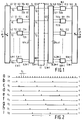
- Figure 2 discloses the functioning of the first and second commutator means 3 and 19 respectively.
- the signal IN applied to the input terminal 1 is given schematically in figure 2(a) as a function of time.
- Figure 2a discloses the samples from which the input signal IN is built up. It discloses only the location of the samples in time, not the amplitude of the samples. The samples are located a time interval T1, which equals 1/F S , apart. The sampling rate of the input signal thus equals F S . In the example of figure 2, it is assumed that M equals 8.
- the signals given in figure 2b to 2i (again only the locations in time, not the amplitudes are given) disclose the signals U7 down to U0 present at the outputs 4.0 to 4.7 respectively of the means 3.
- the means 3 acts in fact as a commutator in that it distributes the eight samples contained each time in consecutive imaginary blocks cyclically to the eight outputs, see also the arrow in the commutator in the block 3 of figure 1.
- the means 19 can also be considered to be a commutator, in that it cyclically couples each of the M inputs 18.0 to 18.7 with the output 20.
- samples present at the inputs 18.0 to 18.M-1 are applied, in the order of the sample present at the input 18.0 first, and the sample present at the input 18.M-1 last, to the output 20 of the commutator means 19. This is shown clearly by means of the arrow in the commutator in the block 19 of figure 1.
- the commutator means 3 can also be built up in a different way, namely by making use of a delay line having tappings at the correct locations along the said delay line. These tappings are then coupled to inputs of decimators, that bring the sampling rate down to the correct value. It is even possible to combine the first commutator means and the analysis filters, expecially by making use of the delay line in the first commutator means 3 for (a part of) the delay line(s) in the analysis filters, which is well known in the art, see USP 4,691,292 (Rothweiler), fig. 3. The same reasoning is in fact valid for the second commutator means 19. In this case interpolators are needed in order to realise the sample rate increase.
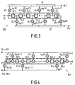
- Figure 3 discloses an embodiment of an analysis filter 6.m.
- An input 30 of the analysis filter which equals the input 5.m in figure 1, is coupled to a series arrangement 31 of delay sections, having equal delays T.
- the delay time T equals the time spacing between the impulses in figure 2.
- Outputs of the odd numbered delay sections 32.1, 32.3, ..., 32.n are coupled to inputs of a first signal combination unit 33.
- Outputs of the even numbered delay sections 32.2, 32.4, ..., are coupled to inputs of a second signal combination unit 34.
- Outputs of the first and second combination units 33 and 34 form the first and second output 35.1 and 35.2 respectively of the analysis filter 6.m. They equal the outputs 7.ma and 7.mb, respectively in fig. 1.
- the input 30 of the filter 6.m is coupled to an input of the second signal combination unit 34 via a multiplication unit 36.1.
- This multiplication unit multiplies the signals (samples) applied to its input by a factor of a m (o).
- the outputs of the odd numbered delay sections are coupled to the inputs of the signal combination unit 33 via multiplication units 36.2, 36.4, ..., 36.n-1 and 36.n+1. They multiply the signals (samples) applied to their respective units by respective factors of a m (1), a m (3), ..., a m (n).
- the outputs of the even numbered delay sections are coupled to the inputs of the signal combination unit 34 via multiplication units 36.3, 36.5, ..., 36.n.
- these multiplication units can be considered as being included in the signal combination units.
- the signal combination units not only realize a summation of the signals applied to their inputs, but they realize a weighted combination (summation) of these signals.
- a multiplication unit has a factor a m (i) that equals zero, the coupling from the delay section to the signal combination unit including the said multiplication unit is dispensed with.
- the said multiplication unit has a factor a m (i) that equals one, the multiplication unit is dispensed with, so that the coupling is a direct coupling.
- the coupling including the multiplication unit 36.n+1 in the filter of figure 3, where n is even is a coupling from the output of the series arrangement 31 to the signal combination unit 34.
- Figure 4 shows a synthesis filter 16.m' having two inputs 50.1 and 50.2 and one output 51.
- the inputs equal the inputs 15.ma and 15.mb and the output equals the output 17.m in figure 1.
- the filter includes a series arrangement 65 of delay sections 66.1 to 66.p, having equal delay T.
- the input 50.1 is coupled to inputs of even numbered delay sections, via multiplication units 67.2, 67.4, ..., 67.p+1. p is thus considered to be an odd number in this example.
- the input 50.2 is coupled to inputs of odd numbered delay sections via multiplication units 67.1, 67.3, ..., 67.p.
- the multiplication coefficients in the multiplicated units 67.1 to 61.p+1 equal b m (P) , b m (p-1) , b m (p-2) , ..., b m (1) and b m (0) respectively.
- Figure 6(c) shows the filterband of the digital signal, which is F S /2 Hz broad. The total filterband is divided into M subbands B0 to B M-1 of equal bandwidth F S /2M.
- Figure 6(a) shows a standard low pass filter or otherwise called: a prototype filter, having a filter characteristic of H(f) and a bandwidth F B equal to half the bandwidth of the subbands.
- Figures 6(d) to (g) show how the multiplication factors for the multiplication units in the filters 6.0 to 6.M-1 can be obtained using the impulse response of the standard low pass filter H(f).
- the factors a0(0) to a M-1 (0) being the multiplication factors for the multiplication units 36.1 in the filters 6.0 to 6.M-1, see Figure 3, equal h0 to h M-1 respectively.
- the factors a0(1) to a M-1 (1) being the multiplication factors for the multiplication units 36.2 in the filters 6.0 to 6.M-1, see Figure 3, equal h M to h 2M-1 respectively,the factors a0(2) to a M-1 (2) equal -h 2M to - h 3M-1 respectively, the factors a0(3) to a M-1 (3) equal -h 3M to -h 4M-1 respectively and so on, see especially the filter in Fig. 6d, which filter is worked out a little bit further.
- the standard filter H(f) can have an odd or an even number of impulses. This means that the filter has an odd or an even number of coefficients h0, h1, h2, ...
- the procedure is such that, if M analysis filters, such as the filter of figure 3 with each filter having a number of n+1 coefficients a m (0) to a m (n) , are needed, an impulse respone h(t) for the standard filter H(f) should be calculated having at most (n+1).M impulses h0, h1, h2, ... In that case there are sufficient coefficients (impulses) in the impulse response h(t) to derive the filter coefficients from this impulse response. If the number of impulses in the standard filter H(f) is less than (n+1)M then zeroes are added before and behind the impulse response, so as to obtain a number of exactly (n+1)M coefficients.
- the method of calculating the filter coefficients b m (0) to b m (p) for the synthesis filters from the coefficients of the standard low pass filter H(f) of figure 6, is as follows.
- Figure 7a to 7d disclose parts of the synthesis filters 16.0, 16.1, 16.m and 16.M-1 respectively.
- each filter having a number of p+1 coefficients b m (0) to b m (p)
- an impulse response h(t) for the standard filter H(f) should be calculated having at most (p+1)M impulses h0, h1, h2, ...
- the impulse response h(t) as given in figure 6a one can derive the filter coefficients for the filters 16.0 to 16.M-1 in the way as shown in figure 7.
- the coefficients b m (0) for the filters 16.0 to 16.M-1 equal the values h0 to h M-1 respectively
- the filter coefficients b m (1) for the filters 16.0 to 16.M-1 equal the values h M to h 2M-1
- the coefficients b m (2) for the filters 16.0 to 16.M-1 equal the values -h 2M to -h 3M-1 , ... and so on.
- the standard filter H(f) for deriving the coefficients for the analysis filters is the same as for the derivation of the coefficients of the synthesis filters. That means that the number of filter coefficients in the analysis filter means equals the number of filter coefficients in the synthesis filter means, and that the coefficients in the analysis filters equal the corresponding coefficients in the synthesis filters.
- FIG. 5a shows an embodiment of the processing unit 9.
- the processing unit 9 includes M signal combination units 70.0 to 70.M-1. 2M inputs, 71.0 to 71.2M-1, of the signal processing unit 9 are coupled via corresponding multiplication units that multiply the samples applied to the inputs 71.0 to 71.2M-1 with factors ⁇ (0,0) to ⁇ (0,2M-1) respectively, to corresponding inputs of the combination unit 70.0.
- the 2M inputs of the processing unit are also coupled to inputs of the combination unit 70.2, via corresponding multiplication units that multiply the samples applied to the inputs 71.0 to 71.2M-1 with factors ⁇ (1,0) to ⁇ (1,2M-1) respectively. This goes on for all the other combination units 70.x, where x runs from 0 to M-1 inclusive.
- the y-th input 71.y is coupled to the output 74.x via a corresponding multiplication unit that multiplies the samples applied to the input 71.y with a factor ⁇ (x,y) , and where y runs from 0 to 2M-1 inclusive.
- the inputs 71.0 to 71.2M-1 correspond in that order with the inputs 8.0 to 8.2M-1 in figure 1.
- the outputs 74.0 to 74.M-1 in that order correspond with the outputs 10.0 to 10.M-1 in figure 1.
- FIG. 5b shows an embodiment of the second processing unit 13.
- the processing unit 13 includes 2M signal combination units 78.0 to 78.2M-1.
- M inputs 76.0 to 76.M-1 of the signal processing unit 13 are coupled via corresponding multiplication units that multiply the samples applied to the inputs 76.0 to 76.M-1 with factors ⁇ (0,0) to ⁇ (0,M-1) respectively to corresponding inputs of the combination unit 78.0.
- the M inputs of the processing unit 13 are also coupled to inputs of the combination unit 78.1 via corresponding multiplication units that multiply the samples applied to the inputs 76.0 to 76.M-1 with factors ⁇ (1,0) to ⁇ (1,M-1) respectively. This goes on for all the other signal combination units.
- v-th input 76.v is coupled to the u-th output via a corresponding multiplication unit that multiplies the samples applied to the input 76.v with a factor ⁇ (u,v) , and the u-th combination unit 78.u, where v runs from 0 to M-1 inclusive.
- the inputs 76.0 to 76.M-1 correspond in that order to the inputs 12.0 to 12.M-1 in figure 1.
- the outputs 77.0 to 77.2M-1 correspond in that order with the outputs 14.0 to 14.2M-1 in figure 1.
- the coefficients ⁇ (x,y) and ⁇ (u,v) can be considered as matrix coefficients in an M x 2M matrix [A] and a 2M x M matrix [B] respectively. Multiplication of both matrices leads to a 2M x 2M matrix [C] having matrix coefficients ⁇ (u,y) for which the following relation holds When using the coefficients for ⁇ (x,y) and ⁇ (u,v) as given in European Patent Application No.
- the standard (or prototype) filter has an odd number of coefficients, it can occur that at least one pair of values (u0,u1) and a corresponding pair of values (y0,y4) are present for which all the coefficients ⁇ (u0,y) , ⁇ (u1,y) , ⁇ (u,y0) and ⁇ (u,y4) , except one, which is ⁇ (u1,y0) , are zero.
- the pair(s) of values (u0,u1) and (y0,y4) again do not overlap with other pairs of values.
- the matrix [C] can further be characterized by the fact that for the remaining 2M-2 values for u and y, there are exactly M-1 separate pairs of value u, such as (u2, u3) and exactly M-1 corresponding separate pairs of values y, such as (y1, y2), for which the coefficients ⁇ (u2,y1) , ⁇ (u2,y2) , ⁇ (u3,y1) and ⁇ (u3,y2) are non zero, the coefficients ⁇ (u2,y) and ⁇ (u3,y) are zero for y not equal to y2 or y3, and the coefficients ⁇ (u,y1) and ⁇ (u,y2) are zero for u not equal to u2 or u3, as specified previously.
- FIG. 8 An example of such a matrix [C] can be found in figure 8.
- the example of figure 8 is for the situation where M equals 32.
- the index u runs vertically from the top down to below along the matrix and the index y runs horizontally from left to right along the matrix.
- the dots in the matrix [C] represent coefficients having a value of zero. For one value of u, u0, which is in the present example equal to 32, all coefficients ⁇ (u0,y) are zero. For one other value u, u1, which is in the present example equal to 33, all coefficients ⁇ (u1,y) are zero except for the coefficient ⁇ (u1,y0) , where y0 equals 32 in the present example.
- the coefficients ⁇ (0,0) and ⁇ (0,1) equal each other and equal c.M/2, or -M/2.
- the coefficients ⁇ (1,0) and ⁇ (1,1) equal each other and equal -c.M/2, or M/2.
- the calculation can result in analysis filters having a number of coefficients that can be larger than or smaller than the number of coefficients in the synthesis filters.
- One partial problem can be derived from the matrix [C] of figure 8 for y having the values 2, 3 and u having the values 2, 3 and 62, 63.
- the relevant circuit path inside the transmission system is indicated by the circuit within the broken lines forming the block 90.1.
- a second partial problem is also given in figure 9. It relates to the circuit path inside the transmission system indicated by the circuit within the broken lines forming the block 90.2.
- a circuit path is given from the input 1, via the commutator 3, a block, such as block 90.1 and the commutator 19 to the output 20.
- the terminal 4.1 of the commutator 3 is coupled to the input of the analysis filter 6.1.
- This analysis filter is coupled to the synthesis filter 16.1 and 16.31 in such a way that the output 7.1a of the analysis filter 6.1 is coupled to the input 15.1b of synthesis filter 16.1 and the input 15.31b of synthesis filter 16.31 via multiplication units that realize a multiplication by a respective factors ⁇ (3,2) and ⁇ (63,2).
- the output 7.1b of the analysis filter 6.1 is coupled to the input 15.1a of synthesis filter 16.1 and the input 15.31a of synthesis filter 16.31 via multiplication units that realize a multiplication by respective factors ⁇ (2,3) and ⁇ (62,3).
- the factors ⁇ (2,3), ⁇ (3,2), ⁇ (62,3) and ⁇ (63,2) can be obtained from the [C] matrix in figure 8.
- a second partial problem is also given in figure 9 and is indicated by the block in broken lines with the reference numeral 90.2.
- the analysis filter 6.2 is coupled to synthesis filters 16.2 and 16.30 in such a way that the output 7.2a is coupled to the input 15.2b of the synthesis filter 16.2 and the input 15.30b of synthesis filter 16.30 via multiplication units that realize a multiplication by respective factors of ⁇ (5,4) and ⁇ (61,4).
- the output 7.2b of synthesis filter 6.2 is coupled to input 15.2a of synthesis filter 16.2 and the input 15.30a of synthesis filter 16.30 via multiplication units that realize a multiplication by respective factors of ⁇ (4,5) and ⁇ (60,5).
- the impulse P1 is applied to the input of analysis filter 6.2. As can be seen from figure 3 this impulse is supplied directly via the multiplication unit 36.1 to the output 35.1, which is the output 7.2a in figure 9. Further impulses are repeatedly supplied to this output 7.2a with time spacings of 2T. This is indicated in figure 10d: the impulse directly supplied to the output 7.2a being indicated by y 4.1 and the next impulse, which is delayed by 2T via the delays 32.1 and 32.2 in figure 3, being indicated by y 4.2 . It can further be seen from figure 3 that the impulse P1 results in impulses at the output 35.2 of the analysis filter, which is the output 7.2b also spaced 2T apart.
- the first impulse which is the impulse y 5.1 in figure 10e, being delayed by a time interval T via the delay 32.1, with reference to the impulse y 4.1 , further impulses, such as the impulse y 5.2 being delayed by the delays 32.2 and 32.3, 32.4 and 32.5, ... and so on.
- the impulse P1 applied to the input 6.1 results in a non delayed impulse y 2.1 at the output 7.1a and further impulses such as the impulse y 2.2 , see figure 10b, spaced 2T apart.
- the impulse P1 further results in an impulse y 3.1 at the output 7.1b spaced a time interval T apart from the impulse y 2.1 and further impulses, such as y 3.2 spaced time intervals 2T apart from y 3.1 see figure 10c.
- the impulse y 2.1 present at the input 8.2 of the processing unit results in impulses u 3.1 , see figure 10g, and u 63.1 , see figure 10m, present at the outputs 14.3 and 14.63 respectively of the processing unit 13.
- the impulse y 4.1 present at the input 8.4 of the processing unit 9 results in impulses u 5.1 , see figure 10i, and u 61.1 , see figure 10k, present at the outputs 14.5 and 14.61 respectively of the processing unit 13.
- the impulse y 3.1 present at the input 8.3 of the processing unit 9 results in impulses u 2.1 , see figure 10f, and u 62.1 , see figure 101, present at the outputs 14.2 and 14.62 respectively of the processing unit 13.
- the impulse y 5.1 present at the input 8.5 of the processing unit 9 results in impulses u 4.1, see figure 10h, and u 60.1 , see figure 10j, present at the outputs 14.4 and 14.60 of the processing unit 13.
- the impulse u 3.1 present at the output 14.3 is applied to the input 15.1b of the synthesis filter 16.1.
- This input is the input 50.2 of the synthesis filter of figure 4.
- This impulse is delayed by a time interval of T in the delay 66.p before it is applied to the output 51, which is coupled to the terminal 18.1 of the commutator 19.
- the impulse u 2.1 present at the output 14.2 is spaced a time interval T apart from the impulse u 3.1 and is applied to the input 15.1a of the synthesis filter 6.1, which is the input 50.1 of the synthesis filter of figure 4.
- This impulse is supplied directly to the output 51 via the multiplication unit 67.p+1.
- the impulse u 4.1 present at the input 15.2a of synthesis filter 16.2, which is the input 50.1 of the synthesis filter in figure 4, is supplied directly via the output of the filter to the terminal 18.2 of the commutator 19.
- the impulse u 5.1 which comes a time interval T earlier than the impulse u 4.1 , is applied to the input 15.2b, which is the input 50.2 of the synthesis filter of figure 4.
- This impulse is delayed by a time interval T in the delay 66.p, so that both impulses u 4.1 and u 5.1 add and are supplied to the terminal 18.2.
- This is indicated in figure 10n by means of the arrow like impulse represented by u 4.1 +u 5.1 , present at the terminal 18.i, with i 2.
- the calculators in the transmission system can be carried out at the end of each time interval T, see figure 2, in which the commutator 3 has supplied one sample to each of the terminals 4.M-1 to 4.0.
- the processing unit 3 has new signals available at all the inputs 8.0 to 8.2M-1, so that the multiplications and summations can be carried out, leading to new output signals available at the outputs 10.0 to 10.M-1.
- the signals disclosed in figure 10n as a function of the terminal index i also indicate the signals as a function of time that occur during that time interval T at the output 20.
- the other two impulses u 60.1 +u 61.1 and u 62.1 +u 63.1 occur in the correct order at the output 21, compared to the occurrence of the impulses P1 and P2 at the input.
- the arrow like impulse u 60.1 +u 61. in figure 10n results from the arrow like impulse P1 in figure 10a and the impulse u 62.1 +u 63.1 in figure 10n results from the impulse P2 in figure 10a.
- the requirements given above will first be applied to the combination of the analysis filter 6.0 and the synthesis filter 16.0, because this combination is a special case, see the [C] matrix of figure 8.
- This combination is disclosed in figure 12a.
- the input signal to the filter 6.0 is one impulse in the signal U0 given in figure 2i.
- the output signal J o.a (k) at the output 7.0a of filter 6.0 can be written as:
- the output signal J o.b (k) at the output 7.0b of filter 6.0 can be written as:
- the number of equations for L0(k) is n+p+1, whereas there are n+1 unknows a0(0) to a0(n), being the coefficients in the analysis filter 6.0.
- FIG. 11 This means that an impulse applied to the input 1 which runs via the analysis filter 6.2 appears at the output 17.30 of synthesis filter 16.30 and that an impulse applied to the input 1 which runs via the analysis filter 6.1 appears at the output 17.31 of synthesis filter 16.31.
- the top horizontal line indicate the indices i of the outputs 4.i of the means 3 on which subsequent impulses in a block of 32 impulses applied to the input 1 appear after each other in time.
- the lower horizontal line indicates the indices j of the inputs 18.j of the means 19.
- the arrows linking an index on the top horizontal line with an index on the lower horizontal line indicate how the transmission system feeds the impulses applied to the outputs 4.i to the inputs 18.i.
- figure 12b makes clear that the output 14.32 of the signal processing unit 13 can be left out, as well as those elements in the input 13 that realize the multiplications by ⁇ (32,v) .
- the calculations given in the foregoing it is thus possible to calculate the required coefficients for the analysis filters.
- the calculations given in the foregoing can be characterized by the statement that the coefficients for the analysis filters are specially adapted to the coefficients of the synthesis filters chosen, such that a tranmission characteristic is obtained that as good as possible approximates a frequency independent delay and a frequency independent amplification factor for the total transmission system.
- Figure 13 shows distortion results for a number of transmission systems.
- the synthesis filters have remained the same.
- the synthesis filters have a length (a number of coefficients) of 16. That means that the value p in figure 4 equals 15.
- European Patent Application No. 90.201.369.7 PHQ 89.018) it is explained how the 512 coefficients can be derived from the impulse response of the standard filter, namely by adding one impulse (and thus one coefficient) of value zero.
- the distortion in the table has been calculated using the formula with ir(k) the real impulse response of the transmission system and dir(k) the desired impulse response.
- the distortion is given in decibels.
- the table in figure 13 further indicates that by increasing the number of coefficients in the analysis filters, to a number larger than the number of coefficients in the synthesis filters, an even lower distortion can be obtained.
- the receivers can have a lower power consumption and can be made cheaper.
- a transmission system I comprising the transmitter 1 with reference numeral 140 and the receiver 1 with reference numeral 141.
- the M analysis filters in the transmitter 140 each comprise n1+1 filter coefficients and the synthesis filters in the receiver 141 each comprise p1+1 filter coefficients.
- n1 equals p1.
- the coefficients of the filters in the transmitter, as well as the receiver are both derived as given in European Patent Application No. 90.201.369.7. That is: the coefficients for the filters in the transmitter and the receiver are both derived from the same standard filter, having a number of impulses which equals M(n1+1) or M(n1+1)-1 .
- a certain transmission quality can be obtained for this transmission system I.
- an other transmission system II comprising the transmitter with reference numeral 142 and the receiver 141.
- the M analysis filters in the transmitter 2 each comprise n2+1 filter coefficients, where n2 > P1.
- the filter coefficients of the analysis filters of transmitter 142 have been obtained in the way as disclosed hereinbefore. This means that the filter coefficients of the analysis filters of transmitter 142 are specially adapted to the filter coefficients of the synthesis filters of receiver 141.
- the transmission system II comprising the transmitter 142 and the receiver 141 realize an improved transmission quality compared to the transmission system I, as has been explained in the foregoing.
- Figure 14 discloses again another transmission system III, comprising the transmitter 140 and a receiver 143.
- This receiver 143 has M synthesis filters, each synthesis filter having p2+1 filter coefficients, where p2 > n1.
- the coefficients of the analysis filters in the transmitter 1 are derived from the standard filter H(f) and thus known and the coefficients of the synthesis filters in the receiver 2 should be determined by means of a calculation procedure equivalent to the one given hereinbefore.
- the filter coefficients of the synthesis filters of receiver 143 are specially adapted to the filter coefficients of the analysis filters in the transmitter 140.
- This also leads to an improved transmission quality for the transmission system III compared to the transmission system I. If p2 equals n2 the transmission quality of the transmission systems II and III are about the same.
- the transmission systems according to the invention realize a better transmission quality than the transmission quality of the transmission system I, in spite of the fact that the transmission system II includes the receiver 141 of the transmission system I and that the transmission system III includes the transmitter 140 of transmission system I.
- the one receiver is the receiver 141, which can be considered to be a receiver for the low end market, and the second receiver being the receiver 143, which can be considered to be a high end version receiver.
- a second possibility is, that only one receiver, such as the receiver 141 is commercially available, whereas two transmitters are present at the transmitter side, namely the transmitter 140 and the transmitter 142.
- the broadcasting authority can now decide on whether to transmit signals via the transmitter 140, or via the transmitter 142, so that reception at the receiver side is either with a low or with an improved signal quality. The same can of course be done in producing prerecorded tapes or discs.
- Figures 15 and 16 show a transmission via magnetic record carriers.
- Figure 15 shows a digital signal recording apparatus, which includes the transmitter as shown in figure 1.
- the apparatus further includes recording means 120 having M inputs 121.0 to 121.M-1, each one coupled to a corresponding one of the M outputs of the signal processing unit 9.
- the apparatus is for recording a digital audiosignal to be applied to the input 1 on a magnetic record carrier 122 by means of at least one magnetic recording head 123.
- the recording means 120 can be an RDAT type of recording means, which uses the helical scan recording principle to record the signal s0 to s M-1 in slant tracks lying next to each other on the record carrier, in the form of a magnetic tape. In that case it might be necessary for the recording means 120 to incorporate means to realize a parallel-to-serial conversion on the signal applied to the inputs 121.1 to 121.M-1.
- the recording means 120 can equally well be an SDAT type of recording means, in which the signals s0 to s m-1 to be recorded are divided over a number of tracks, the said number of tracks not necessarily being equal to M, lying in parallel on, and in the length direction of the record carrier. Also in this case it might be necessary to realize parallel-to-serial conversion on the signals, e.g. if the number of tracks is less than M.
- RDAT and SDAT type of recording means are well known in the art and can e.g. be found in the book "The art of digital audio" by J. Watkinson, Focal press, London, 1988. Therefore no further explanation is needed.
- Figure 16 shows a digital reproduction apparatus, which includes the receiver as shown in figure 1.
- the apparatus further includes reproducing means 124 having M outputs 125.0 to 125.M-1, each one coupled to one of the inputs 12.0 to 12.M-1 of the other signal processing unit 13.
- the apparatus is for reproducing the digital signal, as it is recorded on the record carrier 122 by means of the apparatus of figure 15. Therefore the reproducing means 124 comprise at least one read head 126.
- the reproducing means can be an RDAT or SDAT type reproducing means.
- the reproducing means in the form of an RDAT or SDAT type reproducing means reference is made to the previously mentioned books of J. Watkinson.
- the analysis filters in the recording apparatus of figure 15 can have a number of filter coefficients that is larger than the number of coefficients in the synthesis filters in the reproducing apparatus. If the reproducing apparatus of figure 16 is incorporated in a playback only apparatus, such apparatus can then be made less expensive and require a lower power consumption.
- the number of filter coefficients in the recording apparatus is smaller than the number of coefficients in the synthesis filters in the reproducing apparatus.
- Apparatuses for recording and reproducing a digital audio signal in/from a record carrier comprise a combination of the recording apparatus of figure 15 and the reproducing apparatus of figure 16.
- the recording and reproducing apparatus comprise M analysis filters on the recording side and M synthesis filters at the reproducing side, the analysis filters having a number M(n+1) coefficients and the synthesis filters having a number of M(p+1) coefficients, the number of coefficients in the analysis filters not being equal to the number of coefficients in the synthesis filters.
- the invention is not limited to the embodiments disclosed herein.
- the invention equally applies tothose embodiments which differ from the embodiments shown in respect which are not relevant to the invention.
- the present invention can be equally well applied in apparatuses such as they are described in the not yet published Netherlands Patent Applications 88.02.769 (PHN 12.735) and 89.01.032 (PHN 12.903) in which at least two signals are combined into a composite signal, are transmitted, and are split up in at least two signals at the receiver side. Further all the calculations can be carried out in software, using a microprocessor, programmed in the correct way. This means that the transmitter as well as the receiver can be provided with a microprocessor that carries out the filterings and signal processing in software.
Landscapes
- Engineering & Computer Science (AREA)
- Computer Networks & Wireless Communication (AREA)
- Signal Processing (AREA)
- Physics & Mathematics (AREA)
- Computer Hardware Design (AREA)
- Mathematical Physics (AREA)
- Computer Security & Cryptography (AREA)
- Compression, Expansion, Code Conversion, And Decoders (AREA)
- Signal Processing For Digital Recording And Reproducing (AREA)
- Filters That Use Time-Delay Elements (AREA)
- Transmission Systems Not Characterized By The Medium Used For Transmission (AREA)
- Cable Transmission Systems, Equalization Of Radio And Reduction Of Echo (AREA)
- Reduction Or Emphasis Of Bandwidth Of Signals (AREA)
Priority Applications (7)
| Application Number | Priority Date | Filing Date | Title |
|---|---|---|---|
| AT90202911T ATE133820T1 (de) | 1990-11-05 | 1990-11-05 | Digitales übertragungssystem, gerät zur aufnahme und/oder wiedergabe und sender sowie empfänger zur anwendung im übertragungssystem |
| EP90202911A EP0484595B1 (de) | 1990-11-05 | 1990-11-05 | Digitales Übertragungssystem, Gerät zur Aufnahme und/oder Wiedergabe und Sender sowie Empfänger zur Anwendung im Übertragungssystem |
| DE69025188T DE69025188T2 (de) | 1990-11-05 | 1990-11-05 | Digitales Übertragungssystem, Gerät zur Aufnahme und/oder Wiedergabe und Sender sowie Empfänger zur Anwendung im Übertragungssystem |
| US07/667,339 US5235647A (en) | 1990-11-05 | 1991-03-08 | Digital transmission system, an apparatus for recording and/or reproducing, and a transmitter and a receiver for use in the transmission system |
| JP31533591A JP3235668B2 (ja) | 1990-11-05 | 1991-11-01 | デジタル伝送システム及び記録/再生装置並びにデジタル伝送システムに用いられる送信機及び受信機 |
| KR1019910019495A KR100210565B1 (ko) | 1990-11-05 | 1991-11-04 | 디지탈 통신 시스템과 이에 사용되는 송신기 및 수신기, 이를 이용한 기록 및 재생장치 |
| HK168296A HK168296A (en) | 1990-11-05 | 1996-09-12 | A digital transmission system, an apparatus for recording and/or reproducing, and a transmitter and a receiver for use in the transmission system |
Applications Claiming Priority (1)
| Application Number | Priority Date | Filing Date | Title |
|---|---|---|---|
| EP90202911A EP0484595B1 (de) | 1990-11-05 | 1990-11-05 | Digitales Übertragungssystem, Gerät zur Aufnahme und/oder Wiedergabe und Sender sowie Empfänger zur Anwendung im Übertragungssystem |
Publications (2)
| Publication Number | Publication Date |
|---|---|
| EP0484595A1 true EP0484595A1 (de) | 1992-05-13 |
| EP0484595B1 EP0484595B1 (de) | 1996-01-31 |
Family
ID=8205164
Family Applications (1)
| Application Number | Title | Priority Date | Filing Date |
|---|---|---|---|
| EP90202911A Expired - Lifetime EP0484595B1 (de) | 1990-11-05 | 1990-11-05 | Digitales Übertragungssystem, Gerät zur Aufnahme und/oder Wiedergabe und Sender sowie Empfänger zur Anwendung im Übertragungssystem |
Country Status (7)
| Country | Link |
|---|---|
| US (1) | US5235647A (de) |
| EP (1) | EP0484595B1 (de) |
| JP (1) | JP3235668B2 (de) |
| KR (1) | KR100210565B1 (de) |
| AT (1) | ATE133820T1 (de) |
| DE (1) | DE69025188T2 (de) |
| HK (1) | HK168296A (de) |
Cited By (3)
| Publication number | Priority date | Publication date | Assignee | Title |
|---|---|---|---|---|
| EP0600642A3 (de) * | 1992-11-30 | 1995-02-08 | American Telephone & Telegraph | Verfahren und Gerät zum Reduzieren korrelierter Fehler in Teilbandkodiersystemen mit Quantisierern. |
| EP0663735A3 (de) * | 1994-01-14 | 2001-02-21 | Lg Electronics Inc. | Teilbandsynthesefilter |
| US7209565B2 (en) | 1989-06-02 | 2007-04-24 | Koninklijke Philips Electronics N.V. | Decoding of an encoded wideband digital audio signal in a transmission system for transmitting and receiving such signal |
Families Citing this family (9)
| Publication number | Priority date | Publication date | Assignee | Title |
|---|---|---|---|---|
| FR2721461B1 (fr) * | 1994-06-16 | 1996-09-06 | France Telecom | Signal formé d'une pluralité de fréquences porteuses orthogonales organisé de façon à simplifier la réception d'un des signaux source le composant, procédé d'émission et récepteur correspondants. |
| EP0872017A1 (de) * | 1995-11-21 | 1998-10-21 | Koninklijke Philips Electronics N.V. | Kochgerät mit katalytischem brenner |
| US5937150A (en) * | 1997-02-10 | 1999-08-10 | Toshiba America Information Systems, Inc. | LCD panel controlled by two process elements |
| GB9711903D0 (en) * | 1997-06-10 | 1997-08-06 | Philips Electronics Nv | Receiver for independent sideband signals |
| SE519552C2 (sv) * | 1998-09-30 | 2003-03-11 | Ericsson Telefon Ab L M | Flerkanalig signalkodning och -avkodning |
| US6889238B2 (en) * | 2001-06-25 | 2005-05-03 | Lockheed Martin Corporation | Parallel decimator adaptive filter and method for all-rate gigabit-per-second modems |
| US7107301B2 (en) * | 2002-03-11 | 2006-09-12 | International Business Machines Corporation | Method and apparatus for reducing latency in a digital signal processing device |
| US8958510B1 (en) * | 2010-06-10 | 2015-02-17 | Fredric J. Harris | Selectable bandwidth filter |
| ITTO20120530A1 (it) | 2012-06-19 | 2013-12-20 | Inst Rundfunktechnik Gmbh | Dynamikkompressor |
Citations (1)
| Publication number | Priority date | Publication date | Assignee | Title |
|---|---|---|---|---|
| EP0190796A1 (de) * | 1985-02-01 | 1986-08-13 | Telecommunications Radioelectriques Et Telephoniques T.R.T. | Filtersatz für Signalanalyse und Synthese |
Family Cites Families (2)
| Publication number | Priority date | Publication date | Assignee | Title |
|---|---|---|---|---|
| US4691292A (en) * | 1983-04-13 | 1987-09-01 | Rca Corporation | System for digital multiband filtering |
| US5109417A (en) * | 1989-01-27 | 1992-04-28 | Dolby Laboratories Licensing Corporation | Low bit rate transform coder, decoder, and encoder/decoder for high-quality audio |
-
1990
- 1990-11-05 EP EP90202911A patent/EP0484595B1/de not_active Expired - Lifetime
- 1990-11-05 AT AT90202911T patent/ATE133820T1/de not_active IP Right Cessation
- 1990-11-05 DE DE69025188T patent/DE69025188T2/de not_active Expired - Fee Related
-
1991
- 1991-03-08 US US07/667,339 patent/US5235647A/en not_active Expired - Lifetime
- 1991-11-01 JP JP31533591A patent/JP3235668B2/ja not_active Expired - Fee Related
- 1991-11-04 KR KR1019910019495A patent/KR100210565B1/ko not_active Expired - Fee Related
-
1996
- 1996-09-12 HK HK168296A patent/HK168296A/en not_active IP Right Cessation
Patent Citations (1)
| Publication number | Priority date | Publication date | Assignee | Title |
|---|---|---|---|---|
| EP0190796A1 (de) * | 1985-02-01 | 1986-08-13 | Telecommunications Radioelectriques Et Telephoniques T.R.T. | Filtersatz für Signalanalyse und Synthese |
Cited By (4)
| Publication number | Priority date | Publication date | Assignee | Title |
|---|---|---|---|---|
| US7209565B2 (en) | 1989-06-02 | 2007-04-24 | Koninklijke Philips Electronics N.V. | Decoding of an encoded wideband digital audio signal in a transmission system for transmitting and receiving such signal |
| US7565298B2 (en) | 1989-06-02 | 2009-07-21 | Koninklijke Philips Electronics N.V. | Record carrier having an encoded wide-band digital audio signal recorded thereon |
| EP0600642A3 (de) * | 1992-11-30 | 1995-02-08 | American Telephone & Telegraph | Verfahren und Gerät zum Reduzieren korrelierter Fehler in Teilbandkodiersystemen mit Quantisierern. |
| EP0663735A3 (de) * | 1994-01-14 | 2001-02-21 | Lg Electronics Inc. | Teilbandsynthesefilter |
Also Published As
| Publication number | Publication date |
|---|---|
| JPH0563661A (ja) | 1993-03-12 |
| US5235647A (en) | 1993-08-10 |
| KR920011126A (ko) | 1992-06-27 |
| JP3235668B2 (ja) | 2001-12-04 |
| DE69025188T2 (de) | 1996-11-07 |
| ATE133820T1 (de) | 1996-02-15 |
| EP0484595B1 (de) | 1996-01-31 |
| DE69025188D1 (de) | 1996-03-14 |
| KR100210565B1 (ko) | 1999-07-15 |
| HK168296A (en) | 1996-09-20 |
Similar Documents
| Publication | Publication Date | Title |
|---|---|---|
| EP0400755B1 (de) | Digitales Übertragungssystem unter Verwendung der Teilbandkodierung eines digitalen Signals | |
| US4829378A (en) | Sub-band coding of images with low computational complexity | |
| CN100375474C (zh) | 强度立体声编译码的传送系统、发射机、接收机及方法 | |
| EP0484595B1 (de) | Digitales Übertragungssystem, Gerät zur Aufnahme und/oder Wiedergabe und Sender sowie Empfänger zur Anwendung im Übertragungssystem | |
| AU672729B2 (en) | Method and device for encoding signal, method and device for decoding signal and recording medium | |
| EP0653846A1 (de) | Verfahren und vorrichtung zum kodieren oder dekodieren von signalen und aufzeichnungsmedium | |
| EP0663739A1 (de) | Digitales signalkodierungsgerät, dazugehöriges dekodiergerät und aufzeichnungsträger | |
| US5327366A (en) | Method for the adaptive filtering of a transformed signal in sub-bands and corresponding filtering method | |
| KR940016074A (ko) | 디지탈 신호 처리 장치와 방법 및 기록매체 | |
| KR940023043A (ko) | 압축데이터 기록 및/또는 재생 혹은 전송 및/또는 수신장치, 방법 및 기록 매체 | |
| EP0713295A1 (de) | Verfahren und vorrichtung zum kodieren und dekodieren von nachrichten und nachrichtenaufzeichnungsträger | |
| GB1585981A (en) | Integer weighted impulse equivalent coded signal processing apparatus | |
| EP0542196A2 (de) | Einrichtung zur Aufzeichnung und Wiedergabe eines digitalen Videosignals | |
| EP0612155B1 (de) | Kodierverfahren, Kodierer und Dekodierer für ein Digitalsignal | |
| US5469517A (en) | Motion compensation circuit | |
| US5375171A (en) | Transmission system, and transmitter and receiver used in the transmission system for transmitting and receiving digital signals containing modulated bit allocation information | |
| EP0500159B1 (de) | Übertragungssystem und Empfänger zur Verwendung im Übertragungssystem | |
| EP0793875B1 (de) | Übertragungssystem mit zeitabhängigen filterbänken | |
| EP0773634B1 (de) | Audio-Teilbandkodierverfahren | |
| EP0730271A1 (de) | Verfahren und Gerät zur Aufzeichnung von digitalen Signalen, Medium zur Aufzeichnung von digitalen Signalen, und Verfahren und Gerät zum Übertragen von digitalen Signalen | |
| EP0554934B1 (de) | Übertragung von digitalen Breitbandsignalen | |
| US20020118764A1 (en) | Repeated decoding and encoding in subband encoder/decoders | |
| Hjorungnes et al. | Algorithm for jointly optimized analysis and synthesis FIR filter banks | |
| JPH0771009B2 (ja) | ディジタルフィルタ回路および帯域分割伝送方式 | |
| UA73532C2 (en) | Signal coding and decoding system; coder; decoder; data record carrier; method for transmitting wideband digital voice signals |
Legal Events
| Date | Code | Title | Description |
|---|---|---|---|
| PUAI | Public reference made under article 153(3) epc to a published international application that has entered the european phase |
Free format text: ORIGINAL CODE: 0009012 |
|
| AK | Designated contracting states |
Kind code of ref document: A1 Designated state(s): AT BE CH DE DK ES FR GB GR IT LI LU NL SE |
|
| RBV | Designated contracting states (corrected) |
Designated state(s): AT BE DE FR GB |
|
| 17P | Request for examination filed |
Effective date: 19921111 |
|
| 17Q | First examination report despatched |
Effective date: 19950210 |
|
| GRAA | (expected) grant |
Free format text: ORIGINAL CODE: 0009210 |
|
| AK | Designated contracting states |
Kind code of ref document: B1 Designated state(s): AT BE DE FR GB |
|
| PG25 | Lapsed in a contracting state [announced via postgrant information from national office to epo] |
Ref country code: BE Effective date: 19960131 Ref country code: AT Effective date: 19960131 |
|
| REF | Corresponds to: |
Ref document number: 133820 Country of ref document: AT Date of ref document: 19960215 Kind code of ref document: T |
|
| REF | Corresponds to: |
Ref document number: 69025188 Country of ref document: DE Date of ref document: 19960314 |
|
| ET | Fr: translation filed | ||
| PLBE | No opposition filed within time limit |
Free format text: ORIGINAL CODE: 0009261 |
|
| STAA | Information on the status of an ep patent application or granted ep patent |
Free format text: STATUS: NO OPPOSITION FILED WITHIN TIME LIMIT |
|
| 26N | No opposition filed | ||
| REG | Reference to a national code |
Ref country code: FR Ref legal event code: CD |
|
| REG | Reference to a national code |
Ref country code: GB Ref legal event code: IF02 |
|
| PGFP | Annual fee paid to national office [announced via postgrant information from national office to epo] |
Ref country code: FR Payment date: 20041125 Year of fee payment: 15 |
|
| PGFP | Annual fee paid to national office [announced via postgrant information from national office to epo] |
Ref country code: GB Payment date: 20041129 Year of fee payment: 15 |
|
| PGFP | Annual fee paid to national office [announced via postgrant information from national office to epo] |
Ref country code: DE Payment date: 20050118 Year of fee payment: 15 |
|
| PG25 | Lapsed in a contracting state [announced via postgrant information from national office to epo] |
Ref country code: GB Free format text: LAPSE BECAUSE OF NON-PAYMENT OF DUE FEES Effective date: 20051105 |
|
| PG25 | Lapsed in a contracting state [announced via postgrant information from national office to epo] |
Ref country code: DE Free format text: LAPSE BECAUSE OF NON-PAYMENT OF DUE FEES Effective date: 20060601 |
|
| GBPC | Gb: european patent ceased through non-payment of renewal fee |
Effective date: 20051105 |
|
| PG25 | Lapsed in a contracting state [announced via postgrant information from national office to epo] |
Ref country code: FR Free format text: LAPSE BECAUSE OF NON-PAYMENT OF DUE FEES Effective date: 20060731 |
|
| REG | Reference to a national code |
Ref country code: FR Ref legal event code: ST Effective date: 20060731 |