EP0484946A2 - Decodeur pour code 5B6B - Google Patents
Decodeur pour code 5B6B Download PDFInfo
- Publication number
- EP0484946A2 EP0484946A2 EP91118997A EP91118997A EP0484946A2 EP 0484946 A2 EP0484946 A2 EP 0484946A2 EP 91118997 A EP91118997 A EP 91118997A EP 91118997 A EP91118997 A EP 91118997A EP 0484946 A2 EP0484946 A2 EP 0484946A2
- Authority
- EP
- European Patent Office
- Prior art keywords
- bits
- signal
- circuit
- mark rate
- mark
- Prior art date
- Legal status (The legal status is an assumption and is not a legal conclusion. Google has not performed a legal analysis and makes no representation as to the accuracy of the status listed.)
- Granted
Links
Images






Classifications
-
- H—ELECTRICITY
- H04—ELECTRIC COMMUNICATION TECHNIQUE
- H04L—TRANSMISSION OF DIGITAL INFORMATION, e.g. TELEGRAPHIC COMMUNICATION
- H04L25/00—Baseband systems
- H04L25/38—Synchronous or start-stop systems, e.g. for Baudot code
- H04L25/40—Transmitting circuits; Receiving circuits
- H04L25/49—Transmitting circuits; Receiving circuits using code conversion at the transmitter; using predistortion; using insertion of idle bits for obtaining a desired frequency spectrum; using three or more amplitude levels ; Baseband coding techniques specific to data transmission systems
- H04L25/4906—Transmitting circuits; Receiving circuits using code conversion at the transmitter; using predistortion; using insertion of idle bits for obtaining a desired frequency spectrum; using three or more amplitude levels ; Baseband coding techniques specific to data transmission systems using binary codes
- H04L25/4908—Transmitting circuits; Receiving circuits using code conversion at the transmitter; using predistortion; using insertion of idle bits for obtaining a desired frequency spectrum; using three or more amplitude levels ; Baseband coding techniques specific to data transmission systems using binary codes using mBnB codes
Definitions
- the present invention relates to a 5B6B coding rule inverse conversion circuit for digital transmission and, in more detail, to improvement of circuit for detecting the mark rate or ratio of 6B code converted by the 5B6B coding rule conversion method.
- a self-timing system for extracting the timing wave from the receiving pulse train itself is widely used in a regenerative repeater to be used in digital transmission.
- the timing information is sometimes lost on the transmission line, in case the input code series is formed by continuation of zero code such as "000.".
- the 5B6B coding rule conversion is executed to suppress continuation of zero code in order to avoid such disappearance of the timing information.
- the 5B6B coding rule conversion means that a digital signal train is divided into groups, each consisting of five bits, and this 5-bit signal is converted into the 5B6B code signal of six bits in accordance with the 5B6B coding rule conversion pattern shown in Fig. 1.
- the received digital signal train is divided into groups, each consisting of six bits and the original 5-bit signal can be obtained by inverse conversion of the 5B6B coding rule.
- Fig. 2 shows a conventional 5B6B coding rule inverse conversion circuit.
- the conventional 5B6B coding rule inverse conversion circuit detects a mark rate of the 6-bit signal to be converted inversely and thereafterthe 5B6B coding rule inverse conversion is executed reponsive to such detection of mark rate or ratio.
- a mark rate means the rate of "ON" bit, namely a bit of logic value "1" in the six bits. In the figure, it is indicated as fractions such as 1/6, 2/6.
- the conventional 5B6B coding rule inverse conversion circuit is formed by two mark rate detecting circuits 111, 112, one code inverse conversion circuit 113 and two select circuts 114, 115.
- the first mark rate detecting circuiti 111 detects the mark rates not listed in the conversion pattern of Fig.
- the second mark rate detecting circuit 112 detects the mark rates listed in the conversion pattern of Fig. 1, that is, the mark rate 2/6, 3/6 or 4/6 and then outputs the signal S86 when the mark rate is 2/6 or 4/6 and also outputs the signal S87 when the mark rate is 3/6.
- the code inverse conversion circuit 113 converts inversely the signal S81 of the six bits, D1 ⁇ D6 by the 5B6B coding rule inverse conversion method when the signal S86 is outputted from the second mark rate detecting circuit 112 and then outputs such converted signal as the signal S82 of the five bits.
- the first select circuit 114 usually outputs the signal S82 as the signal S83 and outputs the signal S85 (the 5-bit signal from D1 to D5) as the signal S83 when the signal S87 is outputted from the second mark rate detecting circuit 112.
- the second select circuit 115 usually outputs the signal S83 as the signal S84 and outputs the 5-bit digital signal "10101" as the signal S84 when the signal S88 is outputted from the first mark rate detecting circuit 111.
- the mark rate of the 6-bit 5B6B code signal is detected.
- the 6B6B coding rule inverse conversion is executed in accordance with the conversion pattern of Fig. 1.
- the mark rate is 0/6, 1/6, 2/6, 4/6 or 6/6
- the 6-bit 6B6B code signal is converted to the 5-bit signal "10101”.
- Those not listed in the conversion pattern of Fig. 1 correspond to the mark rates 2/6 and 4/6.
- the 5B6B coding rule inverse conversion circuit of the present invention comprises a composition including a first decoder for generating the signal of eight patterns from the upper three bits in the six bits signal which has been converted by the 5B6B coding rule conversion method, a second decoder for generating a signal of eight patterns from the lower three bits in the six bits, a mark rate detecting circuit for detecting a mark rate of six bits from the signal of eight patterns from the first and second decoders, a code inverse conversion circuit for converting the six bits into the 5-bit signal by the 5B6B coding rule inverse conversion responsive to the mark rate detected by the mark rate detecting circuit and a select circuit for selecting and outputting any one signal among the 5-bit signal converted inversely by the code inverse converting circuit, signal of upper five bits in the six bits and error signal, responsive to the mark rate detected by the mark rate detecting circuit.
- Fig. 3 is a block diagram schematically indicating a 5B6B coding rule inverse conversion circuit as the first embodiment.
- 1a and 1b denote a first and a second 3-line to 8-line decoder/demultiplexer (hereinafter abbreviated as 3:8 decoder); 2, a mark rate detecting circuit; 3, a code inverse conversion circuit; 4, a select circuit.
- the first 3:8 decoder 1a generates a converted signal S5 of eight patterns from the upper three bits D1 ⁇ D3 in the signal S1 of six bits D1 ⁇ D6 converted by the 5B6B coding rule conversion method.
- the second 3:8 decoder 1b generates a converted signal S6 of eight patterns from the lower three bits D4 ⁇ D6 in the signal S1 of six bits.
- the mark rate detecting circuit 2 outputs, when the mark rate, namely 2/6 or 4/6, listed in the 5B6B coding rule conversion pattern of Fig. 1 is detected, the signal S7 and also outputs, when the mark rate, namely, 0/6, 1/6, 2/6, 4/6, 5/6 or 6/6, not listed in the conversion pattern of Fig. 1 is detected, the signal S8.
- the mark rates 2/6, 4/6 correspond to those not listed in the conversion pattern of Fig. 1.
- the code inverse conversion circuit 3 inversely converts, when the mark rate detecting circuit 2 outputs the signal S7, the input signal S1 by the 5B6B coding rule inverse conversion method based on the conversion pattern of Fig. 1 and outputs the signal as the 5-bit signal S2.
- the select circuit 4 selects and outputs three kinds of signals, responsive to output content of the mark rate detecting circuit 2. Namely, when the signal S7. is ouputted from the mark rate detecting circuit 2, the select circuit 4 outputs in direct the output signal S2 of the code inverse conversion circuit 3 as the signal S3. When the signal S8 is outputted from the mark rate detecting circuit 2, the select circuit 4 outputs the preset 5-bit signal "10101" as the signal S3. When both the signals S7 and S8 are not outputted from the mark rate detecting circuit 2, the mark rate is considered as 3/6, the select circuit 4 outputs the signal S4 (5-bit signal D1 ⁇ D5) as the signal S3.
- the 6-bit 5B6B code signal S1 is divided into groups of three bits and the first and second 3:8 decoders 1a, 1b generate the converted signals S5, S6 of 16 patterns (eight patterns x 2).
- the mark rate detecting circuit 2 detects all patterns (44 patterns) of the mark rate other than 3/6 and classifies such patterns into the signals, not listed in the conversion pattern shown in Fig. 1, namely the error signal S8 and the signal S7 listed in the conversion pattern of Fig. 1, and the select circuit 4 selects the signal S2 when the signal S7 is detected, or the signal "10101" when the signal S8 is detected, or the signal S4 when both signals S7 and S8 are not detected, to output the 5-bit signal S3.
- the mark rate detecting circuit 2 is not required to detect the mark rate 3/6. Moreover, use of the first and second 3:8 decoders 1a, 1b realizes combination of numerals in detection of mark rate as shown in 1 ⁇ 5 of Fig. 4.
- the mark rate detecting circuit 2 detects the mark rate with the 3-bit signals of D1 ⁇ D3 and D4 ⁇ D6, patterns are overlapped like the patterns (A) ⁇ (L) of each bit patern shown in Fig. 4. It indicates that when the signal of three bits D1 ⁇ D3 is "000", if the signal of three bits D4 ⁇ D6 is any one of the (A) pattern ("001", “101", "100"), the mark rate becomes 1/6, and when the signal of three bits D1 ⁇ D3 is any one of the (H) pattern ("001", "010"), if the signal of three bits D4 ⁇ D6 is any one of the (A) pattern, the mark rate becomes 2/6.
- the mark rate detecting circuit 2 has a circuit composition suitable for simplification so that when the (A) pattern is detected, as indicated by 1 ⁇ 5 of Fig. 4, if the signal of three bits D1 D3 is "000", the mark rate is 1/6 and if the (H) pattern is detected, the mark rate is 2/6.
- the code inverse conversion circuit 3 inputs in direct the 6-bit signal S1 when the mark rate 2/6 is detected and inputs the signal S1 after polarity inversion when the mark rate is 4/6.
- the inverse conversion is executed by detecting only the pattern with the mark rate 2/6. In this case, since the number of "1" is two when the mark rate is 2/6, the inverse conversion is executed easily in the circuit depending on the position of "1".
- the select circuit 4 five 3-line to 1-line type select circuits (hereinafter abbreviated as 3:1 select circuit) are used in place of 10 conventional 2-line to 8-line type select circuits.
- This select circuit 4 is necessary for all five bits of the output signal S3 and two stages of select circuits have been employed. Therefore the circuit scale has been large. But, use of the 3:1 select circuit has realized scale-down of circuit structure and reduction of redundant circuits.
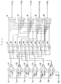
- Fig. 5 is a circuit diagram of the first and second 3:8 decoders 1a, 1b. As shown in this figure, the 5B6B code signals S11 ⁇ S18 of six bits D1 ⁇ D6 are inputted in unit of thre bits and are then converted into the signals S50 ⁇ S57 and S60 ⁇ S67 of eight patterns.
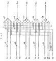
- Fig. 6 indicates a circuit diagram of the part 2A for detecting the mark rates 0/6, 1/6, 2/6, 4/6, 5/6, 6/6 of the mark rate detecting circuit 2.
- the mark rates 0/6, 1/6 indicated by 1 of Fig. 4 are detected by respectively inputting the output signal of the AND circuit 25 for detecting (A) pattern of Fig. 4 and the output signal S50 of decoder 1a, and also inputting the output signal of AND circuit 21 for detecting (C) pattern of Fig. 4 and the output signal S60 of decoder 1b to the NAND circuit 22.
- the mark rates 5/6, 6/6 indicated by 2 of Fig. 4 are detected by respectively inputting the output signal of AND circuit 26 for detecting (B) pattern of Fig. 4 and the output signal S57 of decoder 1a, and also inputting the output signal of AND circuit 23 for detecting (D) pattern of Fig. 4 and the output signal S67 of decoder 1b to the NAND circuit 24.
- the mark rates 2/6, 4/6 indicated by 5 of Fig. 4 are detected by respectively inputting the signals S50, S63, signals S51 S67, signals S53, S66, signals S54, S61, signals S56, S60 ans signals S57, S64 to the NOR circuits 27 ⁇ 2C.
- the mark rates 0/6, 1/6, 2/6, 4/6, 5/6, 6/6 not listed in the conversion pattern of Fig. 1 are detected as the error by the NOR circuit 2D, NOR circuit 2E and NAND circuit 2F and the error detection signal S8 is outputted.
- Fig. 7 is an electrical circuit of the part 2B for detecting the mark rates 2/6 and 4/6 of the mark rate detecting circuit 2.
- the mark rate indicated by 3 of Fig. 4 is detected as explained hereunder.
- the patterns (E) ⁇ (H) of Fig. 4 are detected by four AND circuits 2R ⁇ 2U.
- the pattern (E) is detected by inputting the signals S65 and S66 to the AND circuit 2R
- the pattern (F) is detected by inputting the signals S62 and S64 to the AND circuit 2T
- the pattern (G) is detected by inputting the signals S53 and S55 to the AND circuit 2U
- the pattern (H) is detected by inputting the signals S51 and S52 to the AND circuit 2S.
- the mark rate 4/6 indicated by 4 of Fig. 4 is detected as explained hereunder. That is, four AND circuits 2V ⁇ 2Y detect the patterns (I) ⁇ (L) of Fig. 4.
- the (I) pattern is detected by inputting the signals S61 and S62 to the AND circuit 2V
- the (J) patern by inputting the signals S63 and S65 to the AND circuit 2W
- the (K) pattern by inputting the signals S52 and S54 to the AND circuit 2X
- the (L) pattern by inputting the signals S55 and S56 to the AND circuit 2Y.
- the mark rate 4/6 is detected by inputting these signals to the NOR circuit 2P.
- the detected sisgnal S72 of the mark rates 2/6 and 4/6 is also outputted by inputting the detected signal S71 of mark rate 2/7 and the detected signal of mark rate 4/6 to the NAND circuit 2Q.
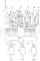
- Fig. 8 is a circuit diagram indicating a practical example of a code inverse conversion circuit 3.
- Detection of individual bit pattern of mark rate 2/6 is executed responsive to the position of a couple of "1" in the 5B6B code signals S11 ⁇ S16 of six bits. This detection is carried out by the NAND circuits 37 ⁇ 3H and this NAND circuit 37 ⁇ 3H also output the signals S21 ⁇ S25 converted in the NAND circuits 3I ⁇ 3M by the detected pattern.
- Fig. 9 is a detail circuit diagram of the select circuit 4. As shown in this figure, the select circuits 41 ⁇ 45 are controlled by a couple of control signals.
- the one control signal is the detected signal S72 of the mark rates 2/6 and 4/6 explained above and the other control signal is the error detection signal S8 explained above.
- Fig. 10 is a diagram for explaining the fundamental composition of the second embodiment of the present invention.
- the 5B6B coding rule inverse conversion circuit of this embodiment comprises a first mark rate detecting circuit 51 for detecting the mark rate of upper three bits D1 ⁇ D3, a second mark rate detecting circuit 52 for detecting mark rate of lower three bits D4 ⁇ D6 and a 6-bit mark rate deciding circuit 53 for deciding the mark rate of six bits D1 ⁇ D6 from the mark rate detected by the first and second mark rate detecting circuits 51, 52.
- This embodiment shows only the circuit portion for detecting the mark rate of six bits.
- the 5B6B code signal of six bits D1 ⁇ D6 is divided into two groups of three bits as in the case of the preceding embodiment.
- logical sum (OR), logical product (AND) and exclusive logical sum (EOR) are taken for individual three bits without using the 3:8 decoder in order to detect respective mark rates.
- the mark rate of three bits can be detected under the conditions:
- the mark rate of six bits as shown in Fig. 13 can be obtained from combination of the mark rates.
- the mark rate 0/6 of six bits can be obtained from combination, for example, of the mark rate 0/3 of upper three bits and the mark rate 0/3 of lower three bits.
- the mark rate 3/6 of six bits can be obtained from combination of the mark rate 0/3 of upper three bits and the mark rate 3/3 of lower three bits.
- the mark rate 6/6 of six bits can be obtained from combination of the mark rate 3/3 of upper three bits and the mark rate 3/3 of lower three bits.
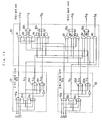
- Fig. 14 shows a practical example of the circuit shown in Fig. 10.
- the first mark rate detecting circuit 51 is formed by a NOR circuit 51a, an AND circuit 51b, an EOR circuit 51c, a NOR circuit 51d and a NOR circuit 51e.
- the second mark rate detecting circuit 52 is formed by a NOR circuit 52a, an AND circuit 52b, an EOR circuit 52c, a NOR circuit 52d and a NOR circuit 52e. These two mark rate detecting circuits 51 and 52 are so-called half-adder circuits.
- a 6-bit mark rate deciding circuit 53 is formed by 12 AND circuits 61 ⁇ 69, 6A ⁇ 6C and four OR circuits 53a, 53b, 53c, 53d.
- the 6-bit 5B6B code signal is divided into the upper three bits and lower three bits and the mark rate of the 5B6B code signal is detected from these patterns.
- a number of detected patterns can be reduced in number and the circuit composition can be scaled down more than that of the conventional circuit.
- the 6-bit 5B6B code signal is divided in unit of two bits.
- the signals of upper and intermediate and lower two bits are respectively applied to a half-adder to detect the mark rate signal of two bits.
- the upper bits signal and lower bits signal of the mark rate signals of these two bits are respectively inputted to different 3:8 decoders so that these decoders generate respectively the converted signals of eight patterns.
- the converted signals of 16 patterns are inputted to the 6-bit mark rate deciding circuit to detect the mark rate of six bits.
- Fig. 15 is a block diagram indicating a fundamental structure of a third embodiment.
- 71, 72, 73 denote a first, a second and a third half-adder; 81, 82, a first and a second 3:8 decoders; 91, a 6-bit mark rate deciding circuit.
- the signals of upper two bits D1, D2 amonog the 5B6B code signals of D1 ⁇ D6 are inputted to the first half-adder 71, the signals of intermediate two bits D3, D4 are inputted to the second half-adder 72 and the signals of lowre two bits D5, D6 are inputted to the third half-adder 73, respectively.
- These three half-adders 71, 72, 73 have the same circuit structure and therefore the circuit of the first half-adder 71 is representatively shown in Fig. 16.
- a half-adder is formed by an exclusive NOR circuit 711 and an OR circuit 712.
- circuits make logical sum (OR) of the signals of upper two bits D1, D2 to be applied to a couple of input terminals A, B and detect the mark rate of two bits from combination of logical values outputted from the output terminals XS, XC of both circuits.
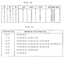
- Fig. 17 shows relationship between the logical values of half-adders and mark rate of two bits.
- the logical value signal of output terminal XS of half-adder is defined as the upper bit signal of 2-bit mark rate signal and the logical value signal of output terminal XC as the lower bit signal thereof for the convenience of explanation.
- the first 3:8 decoder 81 respectively inputs the upper bit signal among 2-bit mark rate signals outputted from three half-adders 71 ⁇ 73 and outputs the logical value signal DS1 of eight patterns by demultiplexing the intpu 3-bit logical value signals.
- the second 3:8 decoder 82 respectively inputs the lower bit signal among 2-bit mark rate signals and outputs the logical value signal DS2 of eight patterns.
- Fig. 18 shows logical values between inputs and outputs of these decoders.
- the 6-bit mark rate deciding circuit 91 is formed, as indicated practically in Fig. 19, by 15 inverters 911 ⁇ 925, 11 AND circuits 931 ⁇ 941 and seven OR circuits 951 ⁇ 957 and detects 6-bit mark rates by logical operations of the logical value signals of 32 patterns to be outputted from the first and second 3:8 decoders 81, 82.
- the inverters 911 ⁇ 925 invert polarity of logical value signals outputted from the decoders 81, 82 and the AND circuits 931 ⁇ 941 and OR circuits 951 ⁇ 957 result in the logical product and logical sum of the polarity-inverted signals.
- An output of the inverter 911 is detected as 6-bit mark rate 0/6
- an output of OR circuit 955 is detected as 6-bit mark rate 1/6
- an output of OR circuit 956 is detected as 6-bit mark rate 2/6
- an output of OR circuit 957 is detected as 6-bit mark rate 4/6
- an output of OR circuit 957 is detected as 6-bit mark rate 4/6
- an output of AND circuit 940 is detected as 6-bit mark rate 5/6
- an output of AND circuit 941 is detected as 6-bit mark rate 6/6, respectively.
- Fig. 20 shows relationship between the logical values of decoder and 6-bit mark rates, with the relationship between the 5B6B code signals D1 ⁇ D6 and output signals of half-adders.
- the mark rates 1/6, 2/6, 4/6 and 5/6 are representative examples and other mark rates are also detected.
- a number of detected patterns can be reduced to about 20 patterns which are about 1/3 of the conventioanl patterns and thereby the circuit structure can be scaled down. Moreover, with simplification of the circuits, cost reduction can be realized through reductrion of power consumption.
Landscapes
- Physics & Mathematics (AREA)
- Spectroscopy & Molecular Physics (AREA)
- Engineering & Computer Science (AREA)
- Computer Networks & Wireless Communication (AREA)
- Signal Processing (AREA)
- Dc Digital Transmission (AREA)
Applications Claiming Priority (4)
| Application Number | Priority Date | Filing Date | Title |
|---|---|---|---|
| JP304523/90 | 1990-11-09 | ||
| JP2304523A JP2594699B2 (ja) | 1990-11-09 | 1990-11-09 | 5b6b符号則逆変換回路 |
| JP5497791A JP2500949B2 (ja) | 1991-03-19 | 1991-03-19 | 5b6b逆変換マ―ク率判定回路 |
| JP54977/91 | 1991-03-19 |
Publications (3)
| Publication Number | Publication Date |
|---|---|
| EP0484946A2 true EP0484946A2 (fr) | 1992-05-13 |
| EP0484946A3 EP0484946A3 (en) | 1993-05-19 |
| EP0484946B1 EP0484946B1 (fr) | 1998-09-23 |
Family
ID=26395807
Family Applications (1)
| Application Number | Title | Priority Date | Filing Date |
|---|---|---|---|
| EP91118997A Expired - Lifetime EP0484946B1 (fr) | 1990-11-09 | 1991-11-07 | Decodeur pour code 5B6B |
Country Status (3)
| Country | Link |
|---|---|
| US (1) | US5293165A (fr) |
| EP (1) | EP0484946B1 (fr) |
| DE (1) | DE69130249T2 (fr) |
Cited By (3)
| Publication number | Priority date | Publication date | Assignee | Title |
|---|---|---|---|---|
| US5335019A (en) * | 1993-01-14 | 1994-08-02 | Sony Electronics, Inc. | Digital video data quantization error detection as applied to intelligent dynamic companding |
| US5357278A (en) * | 1993-01-14 | 1994-10-18 | Sony Electronics, Inc. | Integrated linear/non-linear static and controllable dynamic companding |
| EP0886407A3 (fr) * | 1992-11-06 | 1998-12-30 | Hewlett-Packard Company | Codage 5B6B pour transmission sur canaux divisés |
Families Citing this family (2)
| Publication number | Priority date | Publication date | Assignee | Title |
|---|---|---|---|---|
| US9495824B2 (en) * | 1997-02-07 | 2016-11-15 | Aim Management, Inc. | Lottery system/electronic gaming device interface and gambling game |
| JP5689498B2 (ja) * | 2013-05-08 | 2015-03-25 | ファナック株式会社 | シリアル通信制御回路 |
Family Cites Families (4)
| Publication number | Priority date | Publication date | Assignee | Title |
|---|---|---|---|---|
| US4189716A (en) * | 1977-03-24 | 1980-02-19 | Bell Telephone Laboratories, Incorporated | Circuit for determining the number of ones in a binary signal |
| SU1023335A1 (ru) * | 1982-01-20 | 1983-06-15 | Предприятие П/Я Г-4220 | Устройство дл определени количества единиц в двоичном числе |
| US4498177A (en) * | 1982-08-30 | 1985-02-05 | Sperry Corporation | M Out of N code checker circuit |
| NL8603164A (nl) * | 1986-12-12 | 1988-07-01 | Optical Storage Int | Werkwijze voor het overdragen van n-bit informatiewoorden, informatieoverdrachtsysteem voor het uitvoeren van de werkwijze, alsmede een kodeerinrichting en dekodeerinrichting voor toepassing in het informatieoverdrachtsysteem. |
-
1991
- 1991-11-05 US US07/787,864 patent/US5293165A/en not_active Expired - Fee Related
- 1991-11-07 EP EP91118997A patent/EP0484946B1/fr not_active Expired - Lifetime
- 1991-11-07 DE DE69130249T patent/DE69130249T2/de not_active Expired - Fee Related
Non-Patent Citations (2)
| Title |
|---|
| ELECTRONICS LETTERS vol. 24, no. 5, 3 March 1988, ENAGE GB pages 274 - 275 PETROVIC '5B6B optical fibre line code bearing auxiliary signals' * |
| IBM JOURNAL OF RESEARCH AND DEVELOPMENT vol. 27, no. 5, September 1983, NEW YORK US pages 440 - 451 WIDMER AND FRANASZEK 'A DC - balanced, partitioned - block, 8B/10B transmission code' * |
Cited By (3)
| Publication number | Priority date | Publication date | Assignee | Title |
|---|---|---|---|---|
| EP0886407A3 (fr) * | 1992-11-06 | 1998-12-30 | Hewlett-Packard Company | Codage 5B6B pour transmission sur canaux divisés |
| US5335019A (en) * | 1993-01-14 | 1994-08-02 | Sony Electronics, Inc. | Digital video data quantization error detection as applied to intelligent dynamic companding |
| US5357278A (en) * | 1993-01-14 | 1994-10-18 | Sony Electronics, Inc. | Integrated linear/non-linear static and controllable dynamic companding |
Also Published As
| Publication number | Publication date |
|---|---|
| DE69130249D1 (de) | 1998-10-29 |
| EP0484946B1 (fr) | 1998-09-23 |
| EP0484946A3 (en) | 1993-05-19 |
| DE69130249T2 (de) | 1999-05-12 |
| US5293165A (en) | 1994-03-08 |
Similar Documents
| Publication | Publication Date | Title |
|---|---|---|
| EP0275585A1 (fr) | Méthode pour la transmission des mots d'information à n-bits, système de transmission d'information pour la mise en oeuvre de cette méthode et appareil de codage et de décodage à utiliser dans le système de transmission d'information | |
| EP0367093A2 (fr) | Code de ligne à courant continu équilibré pour la transmission de données arbitraires | |
| EP0735729B1 (fr) | Procédé de codage 5B4T | |
| EP0040632A4 (fr) | Systeme de traitement de donnees avec transmission serielle de donnees entre des sous systemes. | |
| EP0534605B1 (fr) | Système de conversion d'un nombre binaire à virgule flottante signé et son nombre biniaire en complément à deux | |
| US7205911B2 (en) | Apparatus and method for 8B/10B code-group validity check | |
| EP0484946A2 (fr) | Decodeur pour code 5B6B | |
| GB2175769A (en) | Processing image data | |
| JPH01302946A (ja) | コード・バイオレーション検出回路 | |
| GB2174577A (en) | Digital communication system | |
| EP0582311A2 (fr) | Convertisseur série/parallèle | |
| JP2900943B2 (ja) | デコーダ | |
| JP2594699B2 (ja) | 5b6b符号則逆変換回路 | |
| EP0949780B1 (fr) | Format de trame et méthode et dispositif pour le traitement de trame | |
| KR100202943B1 (ko) | 다치논리데이터송신시스템 | |
| KR960000539B1 (ko) | 동기데이타링크제어/고레벨데이타링크제어(sdlc/hdlc)통신에서의 데이타프레임 동기비트생성장치 | |
| KR100299849B1 (ko) | 시디엠에이 이동통신 시스템의 기지국용 모뎀 출력 디지털조합기 | |
| JPS60253372A (ja) | 画信号符号化方式 | |
| KR0174861B1 (ko) | 음성 신호 부호화 기법 중 마이크로-법칙을 구현한 하드웨어 | |
| KR200232068Y1 (ko) | 고속 동작을 위한 2의 보수 변환 장치 | |
| JPH05114924A (ja) | データ伝送方法およびその装置 | |
| SU1136199A2 (ru) | Устройство дл преобразовани дискретных сигналов | |
| JPH088494B2 (ja) | 符号変換方式 | |
| JPH03104319A (ja) | 誤り検出回路 | |
| JPH05110443A (ja) | デイジタル伝送用復号器 |
Legal Events
| Date | Code | Title | Description |
|---|---|---|---|
| PUAI | Public reference made under article 153(3) epc to a published international application that has entered the european phase |
Free format text: ORIGINAL CODE: 0009012 |
|
| AK | Designated contracting states |
Kind code of ref document: A2 Designated state(s): DE FR GB SE |
|
| PUAL | Search report despatched |
Free format text: ORIGINAL CODE: 0009013 |
|
| AK | Designated contracting states |
Kind code of ref document: A3 Designated state(s): DE FR GB SE |
|
| 17P | Request for examination filed |
Effective date: 19931014 |
|
| 17Q | First examination report despatched |
Effective date: 19960607 |
|
| GRAG | Despatch of communication of intention to grant |
Free format text: ORIGINAL CODE: EPIDOS AGRA |
|
| GRAG | Despatch of communication of intention to grant |
Free format text: ORIGINAL CODE: EPIDOS AGRA |
|
| GRAH | Despatch of communication of intention to grant a patent |
Free format text: ORIGINAL CODE: EPIDOS IGRA |
|
| GRAH | Despatch of communication of intention to grant a patent |
Free format text: ORIGINAL CODE: EPIDOS IGRA |
|
| GRAA | (expected) grant |
Free format text: ORIGINAL CODE: 0009210 |
|
| AK | Designated contracting states |
Kind code of ref document: B1 Designated state(s): DE FR GB SE |
|
| REF | Corresponds to: |
Ref document number: 69130249 Country of ref document: DE Date of ref document: 19981029 |
|
| ET | Fr: translation filed | ||
| PLBE | No opposition filed within time limit |
Free format text: ORIGINAL CODE: 0009261 |
|
| STAA | Information on the status of an ep patent application or granted ep patent |
Free format text: STATUS: NO OPPOSITION FILED WITHIN TIME LIMIT |
|
| 26N | No opposition filed | ||
| PGFP | Annual fee paid to national office [announced via postgrant information from national office to epo] |
Ref country code: GB Payment date: 19991103 Year of fee payment: 9 |
|
| PGFP | Annual fee paid to national office [announced via postgrant information from national office to epo] |
Ref country code: SE Payment date: 19991104 Year of fee payment: 9 |
|
| PGFP | Annual fee paid to national office [announced via postgrant information from national office to epo] |
Ref country code: DE Payment date: 19991108 Year of fee payment: 9 |
|
| PGFP | Annual fee paid to national office [announced via postgrant information from national office to epo] |
Ref country code: FR Payment date: 19991109 Year of fee payment: 9 |
|
| PG25 | Lapsed in a contracting state [announced via postgrant information from national office to epo] |
Ref country code: GB Free format text: LAPSE BECAUSE OF NON-PAYMENT OF DUE FEES Effective date: 20001107 |
|
| PG25 | Lapsed in a contracting state [announced via postgrant information from national office to epo] |
Ref country code: SE Free format text: THE PATENT HAS BEEN ANNULLED BY A DECISION OF A NATIONAL AUTHORITY Effective date: 20001129 |
|
| GBPC | Gb: european patent ceased through non-payment of renewal fee |
Effective date: 20001107 |
|
| EUG | Se: european patent has lapsed |
Ref document number: 91118997.5 |
|
| PG25 | Lapsed in a contracting state [announced via postgrant information from national office to epo] |
Ref country code: FR Free format text: LAPSE BECAUSE OF NON-PAYMENT OF DUE FEES Effective date: 20010731 |
|
| PG25 | Lapsed in a contracting state [announced via postgrant information from national office to epo] |
Ref country code: DE Free format text: LAPSE BECAUSE OF NON-PAYMENT OF DUE FEES Effective date: 20010801 |
|
| REG | Reference to a national code |
Ref country code: FR Ref legal event code: ST |