EP0486128A2 - Optische Halbleiteranordnung und ihr Herstellungsverfahren - Google Patents
Optische Halbleiteranordnung und ihr Herstellungsverfahren Download PDFInfo
- Publication number
- EP0486128A2 EP0486128A2 EP91304792A EP91304792A EP0486128A2 EP 0486128 A2 EP0486128 A2 EP 0486128A2 EP 91304792 A EP91304792 A EP 91304792A EP 91304792 A EP91304792 A EP 91304792A EP 0486128 A2 EP0486128 A2 EP 0486128A2
- Authority
- EP
- European Patent Office
- Prior art keywords
- semiconductor
- layer
- quantum
- occur
- grooves
- Prior art date
- Legal status (The legal status is an assumption and is not a legal conclusion. Google has not performed a legal analysis and makes no representation as to the accuracy of the status listed.)
- Granted
Links
Images


Classifications
-
- H—ELECTRICITY
- H10—SEMICONDUCTOR DEVICES; ELECTRIC SOLID-STATE DEVICES NOT OTHERWISE PROVIDED FOR
- H10H—INORGANIC LIGHT-EMITTING SEMICONDUCTOR DEVICES HAVING POTENTIAL BARRIERS
- H10H20/00—Individual inorganic light-emitting semiconductor devices having potential barriers, e.g. light-emitting diodes [LED]
- H10H20/80—Constructional details
- H10H20/81—Bodies
- H10H20/811—Bodies having quantum effect structures or superlattices, e.g. tunnel junctions
- H10H20/812—Bodies having quantum effect structures or superlattices, e.g. tunnel junctions within the light-emitting regions, e.g. having quantum confinement structures
-
- B—PERFORMING OPERATIONS; TRANSPORTING
- B82—NANOTECHNOLOGY
- B82Y—SPECIFIC USES OR APPLICATIONS OF NANOSTRUCTURES; MEASUREMENT OR ANALYSIS OF NANOSTRUCTURES; MANUFACTURE OR TREATMENT OF NANOSTRUCTURES
- B82Y20/00—Nanooptics, e.g. quantum optics or photonic crystals
-
- H—ELECTRICITY
- H01—ELECTRIC ELEMENTS
- H01S—DEVICES USING THE PROCESS OF LIGHT AMPLIFICATION BY STIMULATED EMISSION OF RADIATION [LASER] TO AMPLIFY OR GENERATE LIGHT; DEVICES USING STIMULATED EMISSION OF ELECTROMAGNETIC RADIATION IN WAVE RANGES OTHER THAN OPTICAL
- H01S5/00—Semiconductor lasers
- H01S5/30—Structure or shape of the active region; Materials used for the active region
- H01S5/34—Structure or shape of the active region; Materials used for the active region comprising quantum well or superlattice structures, e.g. single quantum well [SQW] lasers, multiple quantum well [MQW] lasers or graded index separate confinement heterostructure [GRINSCH] lasers
- H01S5/341—Structures having reduced dimensionality, e.g. quantum wires
Definitions
- the present invention relates to a semiconductor optical element and a manufacturing method therefor and, more particularly, to a semiconductor optical element including a plurality of quantum wires or quantum boxes in its active region and a method for easily fabricating the same.
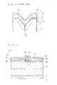
- Figure 2 is a cross-sectional view showing a structure of a quantum wire semiconductor laser device disclosed in a paper by E.Kapon, Applied Physics Letter 55(26), 25th December 1989, pp.2715 to 2717.
- the device of figure 2 includes an n type GaAs substrate 1 patterned with a V-shaped stripe groove An n type AlyGa 1 _yAs cladding layer 2, an Al X Ga 1-x AS first SCH (Separate Confinement Heterostructure) layer 3, a GaAs quantum well layer 4, an Al X Ga 1-x AS second SCH layer 5, a p type Al y Ga 1-y As cladding layer 6, and a p type GaAs contact layer 7 are successively laminated on the substrate 1 keeping the configuration of the V-shaped stripe groove.
- a p side electrode 8 is disposed on the contact layer 7 and an n side electrode (not shown here) is disposed on the entire rear surface of the substrate 1.
- a high resistance region 22 is formed in the p type AlyGa 1 _yAs cladding layer 6 and the p type GaAs contact layer 7 by proton implantation
- a current equal to the threshold current or more is injected in the forward direction to the pn junction of the quantum wire semiconductor laser shown in figure 2, laser oscillation occurs in the well layer 4 and then a laser light is emitted.
- an ordinary semiconductor laser has an active region of approximately 0.05 to 0.2 micron thickness
- a quantum well laser generally has a quantum well layer of approximately 300 angstroms thickness or less. In such quite thin layer, a quantum effect occurs so that electrons are localized in the film thickness direction. As a result, a higher gain is obtained in the quantum well laser than in the ordinary semiconductor laser and effects of reductions in the threshold current and the operation current as improvements in laser characteristics are expected.
- the quantum wire semiconductor laser is obtained by that quantization is also realized in the horizontal direction in addition to the layer thickness direction that is effected in the quantum well laser. This quantum wire semiconductor laser can present more eminent effect of quantization.
- a potential barrier is also formed in the horizontal direction by the epitaxial growth layers on the V-shaped groove. Electrons and holes are confined in the potential barrier and then quantized.
- the length of the quantum wire stripe is approximately 500 angstroms or less, a so-called quantum box in which electrons and holes are confined three-dimensionally is obtained, so that the quantum effect is more eminent.
- the width W z of the quantum wire in the horizontal direction largely depends on the configuration of the V-shaped groove and the rate of the epitaxial growth of the epitaxial growth layers. This makes it quite difficult to control the width W z at high precision.
- the maximum output power of a semiconductor laser is generally limited to a level at which a catastrophic optical damage (hereinafter referred to as COD) of the facet occurs. In order to heighten the COD level to enhance the maximum output power, it is required to increase the cross-sectional area of the light emitting region.
- COD catastrophic optical damage
- Figure 3(a) is a cross-sectional view showing a semiconductor laser device utilizing a two-dimensional multi quantum well structure, disclosed in Japanese Patent Laid-open Application No. 63-29989.
- the device of figure 3(a) has a p type GaAs substrate 31.
- a p type Al o . 3 Ga o . 7 As cladding layer 32 is disposed on the substrate 31.
- a two-dimensional multi-quantum well active layer 37 having stripe configuration, connecting the facets constituting a resonator, is disposed on a center part of the cladding layer 32 in the width direction of the laser device.
- a silicon dioxide (Si0 2 ) insulating film 38 is disposed on the cladding layer 32 and the side walls of the active layer 37.
- An n type Al o . 3 Ga o . 7 As cladding layer 39 is disposed on the insulating film 38 and the active layer 37.
- An n type GaAs contact layer 40 is disposed on the cladding layer 39.
- a p side electrode 42 is disposed on the rear surface of the substrate 31 and an n side electrode 41 is disposed on the contact layer 40.
- Figures 3(b) and 3(c) show the production process of the two-dimensional multi-quantum well active layer 37 shown in figure 3(a).
- cladding layer 32 is crystal grown on the substrate 31. Then, an AIGaAs layer 33A of 50 angstroms thickness and a GaAs layer 33B of 50 angstroms thickness are alternatively laminated ten times respectively on cladding layer 32 to form a laminated structure. Thereafter, photoresist film 34 is patterned on the laminated structure, and then the laminated structure comprising AIGaAs layers 33A and GaAs layers 33B is etched away using photoresist film 34 as a mask. Then, the side surface of the remaining laminated structure is further etched away by a reactive ion etching to form periodical concave parts 33C each having a depth 1 as shown in figure 3(b).
- the depth 1 is 50 angstroms.
- Such etching configuration can be realized because it is possible in reactive ion etching to set the etching rate of AIGaAs about 200 times as high as that of GaAs by setting the etching condition appropriately.
- a GaAs film 37B and an AIGaAs film 37A are alternatively grown by a vapor phase epitaxy.
- respective films are grown on the side surface of the laminated structure reproducing the concavo-convex configuration thereof precisely, as shown in figure 3(c).
- the alternative growths of GaAs film 37B and Al-GaAs film 37A are repeated until the width of active region 37 becomes approximately 0.8 to 1 micron, resulting in the structure shown in figure 3(c).
- the laminated structure comprising AIGaAs layer.33A and GaAs layer 33B is etched away by a usual photolithography technique and a dry etching so as to form active region 37 in a stripe configuration.
- insulating film 38, cladding layer 39 and contact layer 40 are formed thereon and the electrodes 41 and 42 are formed on the contact layer 40 and on the rear surface of substrate 31, respectively.
- the laser structure shown in figure 3(a) is completed.
- GaAs film 37B has a very fine and slender linear configuration whose cross-section has approximately 50 angstroms dimensions for one edge, superior laser characteristics that the threshold value is reduced due to the effect of the quantization of injected carriers can be obtained.
- this prior art structure it is possible to form a plurality of quantum wires in the active layer, so that a laser device having a high output power can be realized.
- the prior art quantum wire semiconductor laser device constituted as described above, several etching processes are required for forming the active layer and, therefore, the production process is quite complicated. In addition, it is quite difficult to apply the prior art quantum wire structure to a general laser device such as a ridge type laser device or an inner stripe type laser device.
- a semiconductor optical element includes a semiconductor substrate or a semiconductor layer formed on a semiconductor substrate; a plurality of stripe-shaped grooves each having a rectangular cross-section whose width is sufficiently narrow to occur a quantum effect, formed on the semiconductor substrate or the semiconductor layer in parallel with each other at an interval sufficiently narrow to occur a quantum effect or a plurality of rectangular-shaped grooves having a width and a length sufficiently narrow to occur a quantum effect, provided on the semiconductor substrate or the semiconductor layer in a checkered arrangement; and a structure in which a quantum well layer whose thickness is less than the depth of the groove and sufficiently thin to occur a quantum effect and a barrier layer whose thickness is larger than the depth of the groove are alternatively laminated, which is provided on the bottom surfaces of the grooves and regions between the adjacent grooves.
- an active region comprising a plurality of quantum wires or quantum boxes can be obtained by a simple production process.
- this quantum wire or quantum box structure can be employed for an active region of a ridge type semiconductor laser, an inner stripe type semiconductor laser or the like.
- a method for manufacturing a semiconductor optical element includes steps of forming a plurality of stripe-shaped grooves each having a rectangular cross-section whose width is sufficiently narrow to occur a quantum effect, on a semiconductor substrate or on a semiconductor layer formed on the substrate in parallel with each other at an interval sufficiently narrow to occur a quantum effect or forming a plurality of rectangular-shaped grooves each having a width and a length sufficiently narrow to occur a quantum effect, on the semiconductor substrate or the semiconductor layer in a checkered arrangement configuration; and alternatively laminating a quantum well layer having a thickness less than the depth of the groove and sufficiently thin to occur a quantum effect and a barrier layer having a thickness larger than the depth of the groove, on the wafer having the grooves with maintaining the concavo-convex configuration of the grooves. Therefore, a laser element having a structure comprising a plurality of quantum wires or quantum boxes can be produced without complicated etching processes or the like.
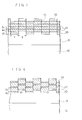
- Figure 1 is a cross-sectional view showing a quantum wire structure of a semiconductor optical element in accordance with an embodiment of the present invention.
- Figure 4 is a cross-sectional view showing a quantum wire structure of a semiconductor optical element in accordance with another embodiment of the present invention.
- reference numeral 12 designates an n type GaAs substrate.
- An n type Al-GaAs cladding layer 9 is disposed on the substrate 12.
- a plurality of stripe-shaped grooves each having a rectangular cross-section of depth di and width x are formed on the cladding layer 9 in parallel with each other at interval y.
- a well layer 10 of thickness W1 and a barrier layer 11 of thickness bi are alternatively laminated on the bottom surface of the stripe-shaped grooves of the cladding layer 9 and on the regions between the adjacent grooves.
- well layer 10 comprises, for example, GaAs and barrier layer 11 comprises, for example, AIGaAs having an energy band gap approximately equal to that of cladding layer 9.
- barrier layer 11 comprises, for example, AIGaAs having an energy band gap approximately equal to that of cladding layer 9.
- AIGaAs cladding layer 9 has a higher energy band gap than that of GaAs well layer 10, so that this cladding layer 9 functions as a barrier layer.
- the depth of groove di, the thickness of well layer W1 and the thickness of barrier layer bi have the following relation; so that the stripe-shaped groove is completely filled up by first well layers 10 and also newly formed grooves are completely filled up by barrier layers 11.
- each well layer 10 is two-dimensionally surrounded by the barrier layers. That is, the upper, lower and both side surfaces thereof are surrounded by the barrier layers.
- the well layer formed on the groove has the same dimension as that of the well layer formed on a region between the adjacent grooves.
- it is required to set the widths x and y and thickness di to approximately 200 angstroms or less.
- the width of stripe-shaped groove d 2 , the thickness of well layer w 2 and the thickness of barrier layer b 2 have the following relation; where the thickness of well layer w 2 is smaller than the thickness of barrier layer b 2 and the half of the sum of w 2 and b 2 is equal to the depth of groove d 2 .
- well layer 10 is positioned at a center part of the adjacent barrier layers 11 in the layer thickness direction and thus well layer 10 is completely surrounded by barrier layers 11. Therefore, the edges of each well layer 10 are not in contact with any edges of other well layer as shown in figure 1, so that the quantum effect is obtained more completely.
- each well layer 10 is three-dimensionally surrounded by barrier layers 11, that is, the upper and lower surfaces, the both side surfaces and the side surfaces perpendicular to the length direction of well layer 10 are surrounded by barrier layers 11 can be obtained.
- the quantum effect is further eminent.
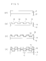
- Figures 5(a) to 5(d) are cross-sectional views showing process steps for producing the quantum wire or quantum box structure in accordance with the embodiment of figure 4.
- a semiconductor layer 9 having an energy band gap corresponding to that of the barrier layer of quantum well structure is epitaxially grown on semiconductor substrate 12.
- portions of semiconductor layer 9 are etched away by a dry etching to form stripe-shaped grooves each having a rectan gular cross-section whose dimension is sufficiently small to occur an effect of quantum wire, or rectangular-shaped grooves arranged in a checkered configuration whose dimension is sufficiently small to occur an effect of quantum box.
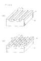
- Figures 6-(a) and 6(b) are perspective views respectively showing a semiconductor layer processed for the quantum wire and a semiconductor layer processed for the quantum box. In these figures, respective dimensions x, y and z are set to approximately 200 angstroms or less.
- first well layer 10 is formed on the grooves and, thereafter, as shown in figure 5(d), first barrier layer 11 is formed on the well layer 10.
- well layer 10 and the barrier layer 11 are alternatively laminated for several times.
- the thicknesses of these layers are set such that the thickness of well layer 10 is smaller than that of barrier layer 11 and the sum of the thickness of barrier layer 11 and the thickness of well layer 10 is twice as large as the depth of the groove.
- the thicknesses of well layer 10 and barrier layer 11 should be equal to the depth of the groove.
- a growth method that can maintain the configuration of the processed semiconductor layer and can form a thin film of 100 angstroms thickness at high reproducibility, for example, a vapor phase epitaxial growth such as MBE (Molecular Beam Epitaxy) or MO-CVD (Metal Organic Chemical Vapor Deposition) is preferably employed.
- MBE Molecular Beam Epitaxy
- MO-CVD Metal Organic Chemical Vapor Deposition
- the quantum wire or quantum box structure of this embodiment has grooves directly formed on the semiconductor layer on the semiconductor substrate and the laminated layer structure is formed thereon, this structure can be easily employed for an active region of a semiconductor laser which can be fabricated by a relatively simple process, such as a ridge type semiconductor laser or an inner-stripe type semiconductor laser. As a result, a high performance quantum wire or quantum box laser device is realized.
- Figures 7(a) and 7(b) are perspective views each showing a semiconductor laser in which the quantum wire structure shown in figure 1 or 4 is employed for an active region thereof, in which figure 7(a) shows a ridge type semiconductor laser and figure 7(b) shows an inner-stripe type semiconductor laser.
- the device of figure 7(a) has an n type GaAs substrate 12.
- An n type AIGaAs lower cladding layer 9 is disposed on substrate 12.
- An active layer 14 including a quantum wire structure is disposed on cladding layer 9.
- a p type AIGaAs upper cladding layer 19 is disposed on active layer 14.
- the cladding layer 19 has a stripe-shaped ridge part which connects cleavage facets 30 and 31.
- a p type GaAs cap layer 20 is disposed on the ridge part of cladding layer 19.
- An n type GaAs current blocking layer 15 is disposed on cladding layer 19 so as to embed the ridge part.
- a p type GaAs contact layer 16 is disposed on current blocking layer 15 and cap layer 20.
- a p side electrode 17 is disposed on contact layer 16 and an n side electrode 18 is disposed on the rear surface of substrate 12.
- a p type AIGaAs first upper cladding layer 29 is disposed on active layer 14.
- An n type GaAs current blocking layer 15 is disposed on first cladding layer 29. This current blocking layer 15 has a stripe-shaped groove serving as a current path.
- a p type AIGaAs second cladding layer 39 is disposed on current blocking layer 15 and first upper cladding layer 29 along the groove configuration of current blocking layer 15.
- a p type GaAs contact layer 16 is disposed on second upper cladding layer 39.
- a p side electrode 17 is disposed on contact layer 16 and an n side electrode 18 is disposed on the rear surface of substrate 12, respectively.
- n type AIGaAs cladding layer 9 is grown on p type substrate 12 by a first crystal growth. Then, grooves for forming quantum wires or quantum boxes shown in figure 6(a) or 6(b) are formed on n type AIGaAs cladding layer 9. Thereafter, a layer serving as a part of n type AIGaAs cladding layer 9 is grown thereon and then quantum wire or quantum box layer 14 comprising a plurality of well layers and barrier layers is grown thereon as described in the embodiments of figures 1 and 4. P type AIGaAs cladding layer 19 and p type GaAs cap layer 20 are grown thereon.
- Figure 8(b) is a cross-sectional view of the wafer in a state after the second crystal growth.
- a Si0 2 film is formed on the surface of the wafer by a sputtering, an electron beam deposition or the like and, thereafter, portions of the Si0 2 film are removed by a photolithography and etching technique to form Si0 2 film 21 in a stripe configuration.
- the thickness and the stripe width of Si0 2 film 21 are, for example, 0.1 to 1.0 micron and 2 to 10 microns, respectively. Hydrofluoric acid or the like is used as etchant for etching the Si0 2 film.
- portions of p type GaAs cap layer 20 and p type AIGaAs cladding layer 19 are removed by etching to form a ridge configuration.
- the width of the bottom part of the ridge is desired to be in a range from 2 microns to 10 microns in view of the control of the transverse mode of laser.
- the ridge part is buried by n type GaAs layer 15 by a third crystal growth.
- Si0 2 film 21 is removed and p type GaAs contact layer 16 is formed on the wafer by a fourth crystal growth.
- n side electrode 18 is formed on the rear surface of substrate 12 and p side electrode 17 is formed on p type GaAs contact layer 16. Thereafter, the wafer is divided into chips, thereby completing laser elements.
- Figure 9(a) is a sectional view of the wafer in a state after the crystal growth.
- n type GaAs current blocking layer 15 by a photolithography and etching technique.
- the surface of p type AIGaAs first upper cladding layer 29 is exposed at the bottom of the groove.
- N type GaAs current blocking layer 15 can be selectively removed using a mixed solution comprising ammonia and hydrogen peroxide as etchant.
- the cross-section of the wafer in this state is shown in figure 9-(b).
- p type AIGaAs second upper cladding layer 39 and p type GaAs contact layer 16 are successively formed on the wafer by a crystal growth.
- n side electrode 18 is formed on the rear surface of substrate 12 and p side electrode 17 is formed on p type GaAs contact layer 16, respectively. Then, the wafer is divided into chips, thereby completing laser elements.
- n type GaAs current blocking layer 15 has both functions of concentrating the current into a region directly below the ridge part or directly below the stripe-shaped groove and of absorbing the laser light generated in the active region from both sides of laser light, to stabilize the horizontal transverse mode.
- quantum wire or quantum box structure is adopted for the active region of such laser structures, a semiconductor laser device having high performances such as low threshold value, low operation current and high speed switching can be obtained.
- the quantum wire or quantum box structure of the present invention can be applied to other semiconductor lasers such as an electrode stripe type laser or a buried hetero type laser.
- the quantum wire or quantum box structure of the present invention can be applied not only to semiconductor lasers but also to semiconductor elements such as a light waveguide or an optical switching element. In these cases, a superior device performance can be realized on the basis of the quantum effect.
- a semiconductor optical element includes a semiconductor substrate or a semiconductor layer formed on a semiconductor substrate; a plurality of stripe-shaped grooves each having a rectangular cross-section whose width is sufficiently narrow to occur a quantum effect, provided on the semiconductor substrate or the semiconductor layer in parallel with each other at interval sufficiently narrow to occur a quantum effect or a plurality of rectangular-shaped grooves having a width and a length sufficiently narrow to occur a quantum effect, provided on the semiconductor substrate or the semiconductor layer in a checkered arrangement; and a structure in which a quantum well layer whose thickness is less than the depth of the groove and sufficiently thin to occur a quantum effect and a barrier layer whose thickness is larger than the depth of the groove are alternatively laminated, which is provided on the bottom surfaces of the grooves formed in the semiconductor substrate or the semiconductor layer and regions between the adjacent grooves.
- an active region comprising a plurality of quantum wires or quantum boxes can be obtained by a simple production process.
- this quantum wire or quantum box structure can be employed for an active region of a ridge type semiconductor laser, an inner stripe type semiconductor laser or the like, whereby a semiconductor laser device having a low threshold value and a low operation current can be easily obtained.
- a plurality of stripe-shaped grooves each having a rectangular cross-section whose width is sufficiently narrow to occur a quantum effect are formed on a semiconductor substrate or on a semiconductor layer on the substrate in parallel with each other at interval sufficiently narrow to occur the quantum effect.
- a plurality of rectangular-shaped grooves each having a width and a length sufficiently narrow to occur a quantum effect are formed on the semiconductor substrate or the semiconductor layer in a checkered arrangement.
- a quantum well layer having a thickness less than the depth of the groove and sufficiently thin to occur a quantum effect and a barrier layer having a thickness larger than the depth of the groove are alternatively laminated on the wafer having the grooves with maintaining the concavo-convex configuration of the grooves. Therefore, a laser device having a structure comprising a plurality of quantum wires or quantum boxes can be produced without complicated etching processes or the like.
Landscapes
- Physics & Mathematics (AREA)
- Engineering & Computer Science (AREA)
- Nanotechnology (AREA)
- Optics & Photonics (AREA)
- Chemical & Material Sciences (AREA)
- Crystallography & Structural Chemistry (AREA)
- Biophysics (AREA)
- Life Sciences & Earth Sciences (AREA)
- Condensed Matter Physics & Semiconductors (AREA)
- General Physics & Mathematics (AREA)
- Electromagnetism (AREA)
- Semiconductor Lasers (AREA)
- Led Devices (AREA)
Applications Claiming Priority (2)
| Application Number | Priority Date | Filing Date | Title |
|---|---|---|---|
| JP31110690A JP2515051B2 (ja) | 1990-11-14 | 1990-11-14 | 半導体光素子及びその製造方法 |
| JP311106/90 | 1990-11-14 |
Publications (3)
| Publication Number | Publication Date |
|---|---|
| EP0486128A2 true EP0486128A2 (de) | 1992-05-20 |
| EP0486128A3 EP0486128A3 (en) | 1992-10-21 |
| EP0486128B1 EP0486128B1 (de) | 1996-03-20 |
Family
ID=18013215
Family Applications (1)
| Application Number | Title | Priority Date | Filing Date |
|---|---|---|---|
| EP91304792A Expired - Lifetime EP0486128B1 (de) | 1990-11-14 | 1991-05-28 | Optische Halbleiteranordnung und ihr Herstellungsverfahren |
Country Status (4)
| Country | Link |
|---|---|
| US (1) | US5126804A (de) |
| EP (1) | EP0486128B1 (de) |
| JP (1) | JP2515051B2 (de) |
| DE (1) | DE69118113T2 (de) |
Cited By (3)
| Publication number | Priority date | Publication date | Assignee | Title |
|---|---|---|---|---|
| WO1995030917A1 (en) * | 1994-05-10 | 1995-11-16 | Massachusetts Institute Of Technology | Three-dimensional periodic dielectric structures having photonic bandgaps |
| EP0665578A3 (de) * | 1993-11-25 | 1996-10-30 | Nippon Telegraph & Telephone | Halbleiterstruktur und Herstellungsverfahren. |
| EP1010997A4 (de) * | 1997-03-29 | 2000-06-21 | Shojiro Kawakami | Dreidimensionale periodische struktur, ihr herstellungsverfahren und verfahren zur filmherstellung |
Families Citing this family (15)
| Publication number | Priority date | Publication date | Assignee | Title |
|---|---|---|---|---|
| JP3124305B2 (ja) * | 1991-03-20 | 2001-01-15 | 富士通株式会社 | 光信号波長選択方法および光波長フィルタ |
| JP3114246B2 (ja) * | 1991-06-07 | 2000-12-04 | ソニー株式会社 | 量子効果デバイス |
| US5175740A (en) * | 1991-07-24 | 1992-12-29 | Gte Laboratories Incorporated | Semiconductor laser and method of fabricating same |
| US5475341A (en) * | 1992-06-01 | 1995-12-12 | Yale University | Sub-nanoscale electronic systems and devices |
| US6320200B1 (en) * | 1992-06-01 | 2001-11-20 | Yale University | Sub-nanoscale electronic devices and processes |
| US5280180A (en) * | 1992-08-19 | 1994-01-18 | Motorola, Inc. | Interconnect structure for coupling semiconductor regions and method for making |
| JP3455987B2 (ja) * | 1993-02-26 | 2003-10-14 | ソニー株式会社 | 量子箱集合素子および情報処理方法 |
| JPH0794707A (ja) * | 1993-09-22 | 1995-04-07 | Sony Corp | 量子素子 |
| US5440421A (en) * | 1994-05-10 | 1995-08-08 | Massachusetts Institute Of Technology | Three-dimensional periodic dielectric structures having photonic bandgaps |
| JPH10506756A (ja) * | 1994-10-05 | 1998-06-30 | マサチューセッツ インスティトゥート オブ テクノロジー | 一次元周期誘導体導波路を使用する共振微小空洞 |
| US5784400A (en) * | 1995-02-28 | 1998-07-21 | Massachusetts Institute Of Technology | Resonant cavities employing two dimensionally periodic dielectric materials |
| JPH09148556A (ja) * | 1995-11-24 | 1997-06-06 | Mitsubishi Electric Corp | 半導体装置,及びその製造方法 |
| JP2007220865A (ja) * | 2006-02-16 | 2007-08-30 | Sumitomo Chemical Co Ltd | 3族窒化物半導体発光素子およびその製造方法 |
| EP2509120A1 (de) * | 2011-04-05 | 2012-10-10 | Imec | Halbleiterbauelement und -verfahren |
| CN115036366A (zh) * | 2021-03-05 | 2022-09-09 | 联华电子股份有限公司 | 半导体装置及其制作方法 |
Family Cites Families (2)
| Publication number | Priority date | Publication date | Assignee | Title |
|---|---|---|---|---|
| JP2531655B2 (ja) * | 1987-01-16 | 1996-09-04 | 株式会社日立製作所 | 半導体装置 |
| JP2575901B2 (ja) * | 1989-11-13 | 1997-01-29 | 新技術事業団 | グリッド入り量子構造 |
-
1990
- 1990-11-14 JP JP31110690A patent/JP2515051B2/ja not_active Expired - Lifetime
-
1991
- 1991-05-28 DE DE69118113T patent/DE69118113T2/de not_active Expired - Fee Related
- 1991-05-28 EP EP91304792A patent/EP0486128B1/de not_active Expired - Lifetime
- 1991-06-03 US US07/710,366 patent/US5126804A/en not_active Expired - Fee Related
Cited By (5)
| Publication number | Priority date | Publication date | Assignee | Title |
|---|---|---|---|---|
| EP0665578A3 (de) * | 1993-11-25 | 1996-10-30 | Nippon Telegraph & Telephone | Halbleiterstruktur und Herstellungsverfahren. |
| WO1995030917A1 (en) * | 1994-05-10 | 1995-11-16 | Massachusetts Institute Of Technology | Three-dimensional periodic dielectric structures having photonic bandgaps |
| US5600483A (en) * | 1994-05-10 | 1997-02-04 | Massachusetts Institute Of Technology | Three-dimensional periodic dielectric structures having photonic bandgaps |
| EP1010997A4 (de) * | 1997-03-29 | 2000-06-21 | Shojiro Kawakami | Dreidimensionale periodische struktur, ihr herstellungsverfahren und verfahren zur filmherstellung |
| US6852203B1 (en) | 1997-03-29 | 2005-02-08 | Autocloning Technology, Ltd | Three-dimensional periodical structure, its manufacturing method, and method of manufacturing film |
Also Published As
| Publication number | Publication date |
|---|---|
| EP0486128A3 (en) | 1992-10-21 |
| DE69118113T2 (de) | 1996-09-12 |
| JPH04180283A (ja) | 1992-06-26 |
| DE69118113D1 (de) | 1996-04-25 |
| US5126804A (en) | 1992-06-30 |
| JP2515051B2 (ja) | 1996-07-10 |
| EP0486128B1 (de) | 1996-03-20 |
Similar Documents
| Publication | Publication Date | Title |
|---|---|---|
| US5126804A (en) | Light interactive heterojunction semiconductor device | |
| US4503540A (en) | Phase-locked semiconductor laser device | |
| EP0663710B1 (de) | Optische Halbleitervorrichtung und Herstellungsverfahren | |
| US5292685A (en) | Method for producing a distributed feedback semiconductor laser device | |
| US5528615A (en) | Semiconductor laser and method of producing the semiconductor laser | |
| US5577062A (en) | Semiconductor laser diode apparatus and method of producing the same | |
| US5786234A (en) | Method of fabricating semiconductor laser | |
| US5149670A (en) | Method for producing semiconductor light emitting device | |
| US5781577A (en) | Semiconductor laser | |
| EP0187718B1 (de) | Halbleiterlaser mit verteilter Rückkopplung | |
| US5173913A (en) | Semiconductor laser | |
| JP2950028B2 (ja) | 光半導体素子の製造方法 | |
| EP0284684B1 (de) | Halbleiterlaser mit umgekehrtem Kanal und ebenem Substrat | |
| US5805628A (en) | Semiconductor laser | |
| US5518954A (en) | Method for fabricating a semiconductor laser | |
| JP3857294B2 (ja) | 半導体レーザ | |
| US5360763A (en) | Method for fabricating an optical semiconductor device | |
| JP2940158B2 (ja) | 半導体レーザ装置 | |
| US5151912A (en) | Semiconductor laser | |
| JP2000101186A (ja) | 半導体光素子およびその製造方法 | |
| JP3057188B2 (ja) | 独立駆動型マルチビームレーザとその製造方法 | |
| JP2822195B2 (ja) | 半導体レーザーの製造方法 | |
| KR100330591B1 (ko) | 반도체레이저다이오드의제조방법 | |
| JP2875440B2 (ja) | 半導体レーザ素子およびその製造方法 | |
| JPH041514B2 (de) |
Legal Events
| Date | Code | Title | Description |
|---|---|---|---|
| PUAI | Public reference made under article 153(3) epc to a published international application that has entered the european phase |
Free format text: ORIGINAL CODE: 0009012 |
|
| AK | Designated contracting states |
Kind code of ref document: A2 Designated state(s): DE FR GB |
|
| PUAL | Search report despatched |
Free format text: ORIGINAL CODE: 0009013 |
|
| AK | Designated contracting states |
Kind code of ref document: A3 Designated state(s): DE FR GB |
|
| 17P | Request for examination filed |
Effective date: 19930215 |
|
| 17Q | First examination report despatched |
Effective date: 19940712 |
|
| GRAA | (expected) grant |
Free format text: ORIGINAL CODE: 0009210 |
|
| AK | Designated contracting states |
Kind code of ref document: B1 Designated state(s): DE FR GB |
|
| REF | Corresponds to: |
Ref document number: 69118113 Country of ref document: DE Date of ref document: 19960425 |
|
| ET | Fr: translation filed | ||
| PLBE | No opposition filed within time limit |
Free format text: ORIGINAL CODE: 0009261 |
|
| STAA | Information on the status of an ep patent application or granted ep patent |
Free format text: STATUS: NO OPPOSITION FILED WITHIN TIME LIMIT |
|
| 26N | No opposition filed | ||
| PGFP | Annual fee paid to national office [announced via postgrant information from national office to epo] |
Ref country code: FR Payment date: 19980511 Year of fee payment: 8 |
|
| PGFP | Annual fee paid to national office [announced via postgrant information from national office to epo] |
Ref country code: GB Payment date: 19980519 Year of fee payment: 8 |
|
| PGFP | Annual fee paid to national office [announced via postgrant information from national office to epo] |
Ref country code: DE Payment date: 19980608 Year of fee payment: 8 |
|
| PG25 | Lapsed in a contracting state [announced via postgrant information from national office to epo] |
Ref country code: GB Free format text: LAPSE BECAUSE OF NON-PAYMENT OF DUE FEES Effective date: 19990528 |
|
| GBPC | Gb: european patent ceased through non-payment of renewal fee |
Effective date: 19990528 |
|
| PG25 | Lapsed in a contracting state [announced via postgrant information from national office to epo] |
Ref country code: FR Free format text: LAPSE BECAUSE OF NON-PAYMENT OF DUE FEES Effective date: 20000131 |
|
| PG25 | Lapsed in a contracting state [announced via postgrant information from national office to epo] |
Ref country code: DE Free format text: LAPSE BECAUSE OF NON-PAYMENT OF DUE FEES Effective date: 20000301 |
|
| REG | Reference to a national code |
Ref country code: FR Ref legal event code: ST |