EP0487739B1 - Halbleiteranordnung und ein verfahren zur herstellung einer solchen halbleiteranordnung - Google Patents
Halbleiteranordnung und ein verfahren zur herstellung einer solchen halbleiteranordnung Download PDFInfo
- Publication number
- EP0487739B1 EP0487739B1 EP91910195A EP91910195A EP0487739B1 EP 0487739 B1 EP0487739 B1 EP 0487739B1 EP 91910195 A EP91910195 A EP 91910195A EP 91910195 A EP91910195 A EP 91910195A EP 0487739 B1 EP0487739 B1 EP 0487739B1
- Authority
- EP
- European Patent Office
- Prior art keywords
- film
- over
- insulating layer
- electrode
- ferroelectric
- Prior art date
- Legal status (The legal status is an assumption and is not a legal conclusion. Google has not performed a legal analysis and makes no representation as to the accuracy of the status listed.)
- Expired - Lifetime
Links
- 239000004065 semiconductor Substances 0.000 title claims abstract description 16
- 238000004519 manufacturing process Methods 0.000 title abstract description 6
- 229910021420 polycrystalline silicon Inorganic materials 0.000 claims abstract description 26
- 229920005591 polysilicon Polymers 0.000 claims abstract description 26
- 238000000034 method Methods 0.000 claims abstract description 17
- 239000000758 substrate Substances 0.000 claims abstract description 16
- 238000005530 etching Methods 0.000 claims abstract description 7
- 229910052763 palladium Inorganic materials 0.000 claims description 2
- 229910052697 platinum Inorganic materials 0.000 claims description 2
- KDLHZDBZIXYQEI-UHFFFAOYSA-N Palladium Chemical compound [Pd] KDLHZDBZIXYQEI-UHFFFAOYSA-N 0.000 claims 2
- BASFCYQUMIYNBI-UHFFFAOYSA-N platinum Chemical compound [Pt] BASFCYQUMIYNBI-UHFFFAOYSA-N 0.000 claims 2
- VYPSYNLAJGMNEJ-UHFFFAOYSA-N Silicium dioxide Chemical compound O=[Si]=O VYPSYNLAJGMNEJ-UHFFFAOYSA-N 0.000 claims 1
- XAGFODPZIPBFFR-UHFFFAOYSA-N aluminium Chemical compound [Al] XAGFODPZIPBFFR-UHFFFAOYSA-N 0.000 claims 1
- 229910052782 aluminium Inorganic materials 0.000 claims 1
- 229910052814 silicon oxide Inorganic materials 0.000 claims 1
- 230000015654 memory Effects 0.000 abstract description 20
- 239000010410 layer Substances 0.000 abstract description 19
- 238000009792 diffusion process Methods 0.000 abstract description 13
- 239000011229 interlayer Substances 0.000 abstract description 6
- 239000000126 substance Substances 0.000 abstract description 6
- 230000015556 catabolic process Effects 0.000 abstract description 3
- 238000009413 insulation Methods 0.000 abstract 1
- 239000003990 capacitor Substances 0.000 description 5
- 239000000463 material Substances 0.000 description 5
- XUIMIQQOPSSXEZ-UHFFFAOYSA-N Silicon Chemical compound [Si] XUIMIQQOPSSXEZ-UHFFFAOYSA-N 0.000 description 4
- 229910052710 silicon Inorganic materials 0.000 description 4
- 239000010703 silicon Substances 0.000 description 4
- 239000012808 vapor phase Substances 0.000 description 4
- 229910003781 PbTiO3 Inorganic materials 0.000 description 2
- OAICVXFJPJFONN-UHFFFAOYSA-N Phosphorus Chemical compound [P] OAICVXFJPJFONN-UHFFFAOYSA-N 0.000 description 2
- 238000005229 chemical vapour deposition Methods 0.000 description 2
- 239000011521 glass Substances 0.000 description 2
- 229910052698 phosphorus Inorganic materials 0.000 description 2
- 239000011574 phosphorus Substances 0.000 description 2
- 238000001020 plasma etching Methods 0.000 description 2
- 230000010287 polarization Effects 0.000 description 2
- 238000004544 sputter deposition Methods 0.000 description 2
- 238000000992 sputter etching Methods 0.000 description 2
- 229910020698 PbZrO3 Inorganic materials 0.000 description 1
- 239000013078 crystal Substances 0.000 description 1
- 230000000694 effects Effects 0.000 description 1
- 238000007687 exposure technique Methods 0.000 description 1
- BHEPBYXIRTUNPN-UHFFFAOYSA-N hydridophosphorus(.) (triplet) Chemical compound [PH] BHEPBYXIRTUNPN-UHFFFAOYSA-N 0.000 description 1
- 238000002347 injection Methods 0.000 description 1
- 239000007924 injection Substances 0.000 description 1
- 230000010354 integration Effects 0.000 description 1
- 238000010030 laminating Methods 0.000 description 1
- 238000000206 photolithography Methods 0.000 description 1
Images
Classifications
-
- H—ELECTRICITY
- H10—SEMICONDUCTOR DEVICES; ELECTRIC SOLID-STATE DEVICES NOT OTHERWISE PROVIDED FOR
- H10B—ELECTRONIC MEMORY DEVICES
- H10B53/00—Ferroelectric RAM [FeRAM] devices comprising ferroelectric memory capacitors
-
- H—ELECTRICITY
- H10—SEMICONDUCTOR DEVICES; ELECTRIC SOLID-STATE DEVICES NOT OTHERWISE PROVIDED FOR
- H10D—INORGANIC ELECTRIC SEMICONDUCTOR DEVICES
- H10D1/00—Resistors, capacitors or inductors
- H10D1/60—Capacitors
- H10D1/68—Capacitors having no potential barriers
- H10D1/682—Capacitors having no potential barriers having dielectrics comprising perovskite structures
Definitions
- the present invention relates to a method for forming a semiconductor device such as a memory, and in particular, an electrically rewritable non-volatile memory having a ferroelectric material.
- the invention also relates to a semiconductor device of the type defined in the preamble of Claim 4.
- a conventional semiconductor non-volatile memory use is commonly made of an MIS-type transistor having a phenomenon that the surface potential of a silicon substrate is modulated by injecting a load from the silicon substrate into a trap in an insulating gate or a floating gate, and the MIS-type transistor is used similarly to an EPROM (ultraviolet ray erasable non-volatile memory), EEPROM (electrically rewritable non-volatile memory), and the like.
- EPROM ultraviolet ray erasable non-volatile memory
- EEPROM electrically rewritable non-volatile memory
- non-volatile memories have disadvantages such as a high information rewriting voltage, typically between 12-20 volts and very long rewriting time (for example, several ten msec in the case of an EEPROM). Moreover, the number of rewriting information rewriting is a problem when the memory is used repetitively.
- non-volatile memory having a ferroelectric material which can electrically inverse polarization
- write-in time and read-out time are substantially the same in principle, and polarization is maintained even if an electric source is cut off, so that this non-volatile memory has as an ideal.
- U.S. Patent No. 4,149,302 proposes a structure integrating a capacitor consisting of a ferroelectric material on a silicon substrate
- U.S. Patent No. 3,832,700 proposes a non-volatile memory wherein a ferroelectric film is on the gate portion of a MIS-type transistor.
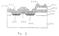
- a non-volatile memory having a structure laminated in a MOS-type semiconductor device such as shown in Fig. 2 was disclosed.
- a P-type Si substrate 201, an element separating LOCOS oxide film 202, an N-type diffusion layer 203, such as a source region, and an N-type diffusion layer 204, such as a drain region, are shown.
- a gate electrode 205, and an interlayer insulating film 206 are also shown.
- a ferroelectric film 207 of a capacitor is formed when sandwiched between a lower electrode 208 and an upper electrode 209.
- a second interlayer insulating film 210, and a wiring electrode 211 comprises Al.
- Such structure of laminating on the upper portion of an MOS-type semiconductor device should distribute wires between the electrode of a ferroelectric film and the high concentration diffusion layer, such as source and drain regions on the semiconductor substrate with the use of Al or other conventional interconnect materials.
- One problem with the prior art, as shown in Fig. 2, is the large amount of area occupied by the transistor and ferroelectric capacitor regions.
- a device is known from European Patent Application EP-A-0 338 157 which discloses a DRAM device comprising a P-type silicon substrate with source and drain regions formed by N+ diffusions, and a gate electrode of doped polysilicon.
- An insulated layer above the substrate has openings over the source and drain regions.
- a capacitor is located above the source region and comprises a lower metallic electrode formed in the opening and in contact with the N+ diffusion, an upper metallic electrode and a dielectric formed by a ferroelectric film located between the two electrodes.
- the object of the present invention is to provide an improved semiconductor device, particularly a low cost non-volatile memory having a small memory cell area and fast information rewriting times, as well as an improved method for the manufacture thereof.
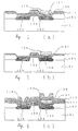
- Figs. 1(a)-(c) are cross-sectional views showing the main steps of one of the preferred embodiments of the method for manufacturing a semiconductor device according to the present invention.
- Fig. 2 is a cross-sectional view of a non-volatile memory according to the prior art.
- Figs. 1(a)-(c) are cross-sectional views showing the main steps of one embodiment of the method for manufacturing a semiconductor device according to the invention.
- the method for manufacturing the semiconductor device according to the invention is explained by reference to Fig. 1.
- Fig. 1 For the sake of explanation, an embodiment having an Si substrate and an N-channel transistor is explained.
- Fig. 1(a) shows a P-type Si substrate 101 and uses a wafer of specific resistance such as 20 ohm-cm.
- An element separating insulating film 102 and an oxide film with a thickness of 6000 ⁇ is formed by a LOCOS method by a known technique.
- An N-type diffusion layer 103 such as a source region, is formed by ion injection of phosphorus at 80 KeV 5x10 15 cm -2 .
- An N-type diffusion layer, such as a drain region, is formed simultaneously with layer 103.
- a gate electrode 105, an interlayer insulating film 111, comprised of 4000 ⁇ of phosphorous glass deposited by chemical vapor deposition (CVD) and a contact hole are formed by conventional photolithography and etch techniques.
- a polysilicon film 106 is formed with a thickness of 5000 ⁇ , by a chemical vapor phase growing method. In this case, the film thickness of the polysilicon film is preferably at least the same as that of said first interlayer insulating film.
- One of electrodes 107 of a ferroelectric film is formed by sputtering Pt, Pd or the like.
- Film 108 comprises of PbTiO 3 , PZT (mixed crystal of PbTiO 3 and PbZrO 3 ), PLZT (La-doped PZT) and the like, and is formed by a sputtering method or the like.
- the ferroelectric film 108 and another electrode 109 are simultaneously etched by a sputter etching.
- a part of the polysilicon film 106 may be etched simultaneously. (See Fig. 1(a)).
- the top electrode 109 of the ferroelectric film and the interconnect layer 110 are formed at the same time and comprise Al.
- a second interlayer insulating film 112 of phosphorus glass having a thickness of 4000 ⁇ is formed by a chemically vapor phase growing method. (see Fig. 1(c)).
- the ferroelectric film is directly formed on the high concentration diffusion layer, and the lower electrode is directly in contact with the high concentration diffusion layer via the polysilicon film, so that the wiring is only needed for the upper electrode, and high integration with a small element area is possible.
- the ferroelectric film thickness is not uniform due to the step difference of the contact hole, and as a result, the ferroelectric capacitor characteristics are degraded reducing the number of read/write cycles to less than 10 5 times. Further, the breakdown voltage is reduced to 12 V.
- a polysilicon film 106 is located between an electrode 107 and a high concentration diffusion layer by a chemical vapor phase growing method, since polysilicon has good adhesivity, the step difference of the contact hole is mitigated, and the film thickness of the ferroelectric film is more uniform improving read/write cycles to 10 10 times, and improving the breakdown voltage to 30 V.
- a non-volatile memory is mainly explained above, but the invention can be applied to a memory (DRAM and the like) with the aid of a large specific dielectric constant of the ferroelectric as a matter of course.
- the present invention comprises the steps of forming a polysilicon film between either one of the electrodes formed by sandwiching a ferroelectric film and a high concentration diffusion layer by a chemical vapor phase growing method, simultaneously etching said electrode and a part of said polysilicon film with the use of sputter etching, and removing the remaining polysilicon film by reactive ion etching, so that the step difference of a contact hole is mitigated, add a film thickness of the ferroelectric film is uniformly formed, and thereby performing an effect of integrating the ferroelectric film having no increase of element area and excellent electrical characteristics.
Landscapes
- Semiconductor Memories (AREA)
- Non-Volatile Memory (AREA)
Claims (7)
- Verfahren zum Ausbilden einer Halbleitervorrichtung, mit den Schrittendes Ausbildens eines Substrates (101) mit einem Source-Bereich (103) und einem Drain-Bereich (104);des Ausbildens einer Gate-Elektrode (105) auf dem Substrat (101) und zwischen dem Source-Bereich (103) und dem Drain-Bereich (104);des Ausbildens einer Isolierschicht (111) auf dem Substrat (101) und um die Gate-Elektrode (105);des Ausbildens einer Kontaktöffnung in der Isolierschicht (111) zum Source-Bereich (103);des Ausbildens einer Polysiliziumschicht (106) direkt über und in direktem Kontakt mit dem Source-Bereich (103) in der Kontaktöffnung, wobei sich die Polysiliziumschicht (106) auch über der Isolierschicht (111) befindet;des Ausbildens einer unteren Elektrode (107) auf der Polysiliziumschicht (106);des Ausbildens einer ferroelektrischen Schicht (108) auf der unteren Elektrode (107);des Ätzens der unteren Elektrode (107) und der ferroelektrischen Schicht (108);des Ätzens der Polysiliziumschicht (106) und der unteren Elektrode (107) durch Ätzen mit kleinem Selektivverhältnis, so daß die Polysiliziumschicht (106) in der Kontaktöffnung verbleibt, und des Ätzens der verbleibenden Polysiliziumschicht (106) durch Ätzen mit großem Selektivverhältnis zu Siliziumoxid, so daß die Polysiliziumschicht (106) auf einem Teil der Isolierschicht (111) verbleibt; unddes Ausbildens einer oberen Elektrode (109) auf der ferroelektrischen Schicht (108).
- Verfahren nach Anspruch 1, wobei die Polysiliziumschicht (106) durch chemisches Aufwachsenlassen der Schicht aus der Gasphase ausgebildet wird und eine Dicke hat, die wenigsten gleich der Dicke der Isolierschicht (111) ist.
- Verfahren nach Anspruch 1, mit den weiteren Schritten des Ausbildens einer zweiten Isolierschicht (112) über der Isolierschicht (111) und des Festlegens einer Anschlußelektrode (110) für den Drain-Bereich (104) in der zweiten Isolierschicht (112).
- Halbleitervorrichtung, miteinem Substrat (101) mit einem Source-Bereich (103) und einem Drain-Bereich (104);einer Gate-Elektrode (105) auf dem Substrat (101) und zwischen dem Source-Bereich (103) und dem Drain-Bereich (104);einer Isolierschicht (111) auf dem Substrat (101) und um die Gate-Elektrode (105);einer unteren Elektrode (107) über dem Source-Bereich (103);einer ferroelektrischen Schicht (108) über der unteren Elektrode (107); undeiner oberen Elektrode (109) auf der ferroelektrischen Schicht (108);dadurch gekennzeichnet, daß
in einer Kontaktöffnung in der Isolierschicht (111) direkt über und in direktem Kontakt mit dem Source-Bereich (103) und über einem Teil der Isolierschicht (111) eine Polysiliziumschicht (106) angeordnet ist; wobei sich die untere Elektrode (107) auf der Polysiliziumschicht (106) befindet. - Vorrichtung nach Anspruch 4, wobei die untere Elektrode (107) aus einem Element aus einer Gruppe besteht, die Platin und Palladium umfaßt.
- Vorrichtung nach Anspruch 4, wobei die ferroelektrische Schicht (108) aus PZT besteht.
- Vorrichtung nach Anspruch 4, wobei die obere Elektrode (109) aus Aluminium besteht.
Applications Claiming Priority (3)
| Application Number | Priority Date | Filing Date | Title |
|---|---|---|---|
| JP143563/90 | 1990-06-01 | ||
| JP02143563A JP3092140B2 (ja) | 1990-06-01 | 1990-06-01 | 半導体装置の製造方法 |
| PCT/JP1991/000735 WO1991019321A1 (fr) | 1990-06-01 | 1991-05-31 | Procede de fabrication de dispostifs a semiconducteurs |
Publications (3)
| Publication Number | Publication Date |
|---|---|
| EP0487739A1 EP0487739A1 (de) | 1992-06-03 |
| EP0487739A4 EP0487739A4 (en) | 1992-10-21 |
| EP0487739B1 true EP0487739B1 (de) | 1996-12-11 |
Family
ID=15341657
Family Applications (1)
| Application Number | Title | Priority Date | Filing Date |
|---|---|---|---|
| EP91910195A Expired - Lifetime EP0487739B1 (de) | 1990-06-01 | 1991-05-31 | Halbleiteranordnung und ein verfahren zur herstellung einer solchen halbleiteranordnung |
Country Status (5)
| Country | Link |
|---|---|
| US (1) | US5229309A (de) |
| EP (1) | EP0487739B1 (de) |
| JP (1) | JP3092140B2 (de) |
| DE (1) | DE69123557T2 (de) |
| WO (1) | WO1991019321A1 (de) |
Families Citing this family (22)
| Publication number | Priority date | Publication date | Assignee | Title |
|---|---|---|---|---|
| EP0516031A1 (de) * | 1991-05-29 | 1992-12-02 | Ramtron International Corporation | Ferroelektrische Stapelspeicherzelle und Herstellungsverfahren |
| JP3374216B2 (ja) * | 1991-10-26 | 2003-02-04 | ローム株式会社 | 強誘電体層を有する半導体素子 |
| US5563081A (en) * | 1992-03-23 | 1996-10-08 | Rohm Co., Inc. | Method for making a nonvolatile memory device utilizing a field effect transistor having a ferroelectric gate film |
| US5352622A (en) * | 1992-04-08 | 1994-10-04 | National Semiconductor Corporation | Stacked capacitor with a thin film ceramic oxide layer |
| EP0784347A2 (de) * | 1992-06-18 | 1997-07-16 | Matsushita Electronics Corporation | Halbleiterbauelement mit Kondensator |
| JP3407204B2 (ja) * | 1992-07-23 | 2003-05-19 | オリンパス光学工業株式会社 | 強誘電体集積回路及びその製造方法 |
| US5330931A (en) * | 1993-09-22 | 1994-07-19 | Northern Telecom Limited | Method of making a capacitor for an integrated circuit |
| US5443688A (en) * | 1993-12-02 | 1995-08-22 | Raytheon Company | Method of manufacturing a ferroelectric device using a plasma etching process |
| US6013950A (en) * | 1994-05-19 | 2000-01-11 | Sandia Corporation | Semiconductor diode with external field modulation |
| US5739563A (en) * | 1995-03-15 | 1998-04-14 | Kabushiki Kaisha Toshiba | Ferroelectric type semiconductor device having a barium titanate type dielectric film and method for manufacturing the same |
| JP3279453B2 (ja) * | 1995-03-20 | 2002-04-30 | シャープ株式会社 | 不揮発性ランダムアクセスメモリ |
| US5920453A (en) * | 1996-08-20 | 1999-07-06 | Ramtron International Corporation | Completely encapsulated top electrode of a ferroelectric capacitor |
| US5702956A (en) * | 1996-08-26 | 1997-12-30 | Taiwan Semiconductor Manufactoring, Company Ltd | Test site and a method of monitoring via etch depths for semiconductor devices |
| US5900644A (en) * | 1997-07-14 | 1999-05-04 | Taiwan Semiconductor Manufacturing Company, Ltd. | Test site and a method of monitoring via etch depths for semiconductor devices |
| US6128211A (en) * | 1997-11-06 | 2000-10-03 | National Science Council | Structures of a low-voltage-operative non-volatile ferroelectric memory device with floating gate |
| JPH11330378A (ja) | 1998-05-19 | 1999-11-30 | Murata Mfg Co Ltd | 半導体装置 |
| US6242299B1 (en) | 1999-04-01 | 2001-06-05 | Ramtron International Corporation | Barrier layer to protect a ferroelectric capacitor after contact has been made to the capacitor electrode |
| US6956274B2 (en) * | 2002-01-11 | 2005-10-18 | Analog Devices, Inc. | TiW platinum interconnect and method of making the same |
| US9846664B2 (en) | 2010-07-09 | 2017-12-19 | Cypress Semiconductor Corporation | RFID interface and interrupt |
| US8723654B2 (en) | 2010-07-09 | 2014-05-13 | Cypress Semiconductor Corporation | Interrupt generation and acknowledgment for RFID |
| US9092582B2 (en) | 2010-07-09 | 2015-07-28 | Cypress Semiconductor Corporation | Low power, low pin count interface for an RFID transponder |
| US9520445B2 (en) * | 2011-07-12 | 2016-12-13 | Helmholtz-Zentrum Dresden-Rossendorf E. V. | Integrated non-volatile memory elements, design and use |
Family Cites Families (7)
| Publication number | Priority date | Publication date | Assignee | Title |
|---|---|---|---|---|
| US5024964A (en) * | 1970-09-28 | 1991-06-18 | Ramtron Corporation | Method of making ferroelectric memory devices |
| US4149301A (en) * | 1977-07-25 | 1979-04-17 | Ferrosil Corporation | Monolithic semiconductor integrated circuit-ferroelectric memory drive |
| US4437139A (en) * | 1982-12-17 | 1984-03-13 | International Business Machines Corporation | Laser annealed dielectric for dual dielectric capacitor |
| US5046043A (en) * | 1987-10-08 | 1991-09-03 | National Semiconductor Corporation | Ferroelectric capacitor and memory cell including barrier and isolation layers |
| US4888630A (en) * | 1988-03-21 | 1989-12-19 | Texas Instruments Incorporated | Floating-gate transistor with a non-linear intergate dielectric |
| JPH01251760A (ja) * | 1988-03-31 | 1989-10-06 | Seiko Epson Corp | 強誘電体記憶装置 |
| DE3850567T2 (de) * | 1988-04-22 | 1994-11-03 | Ramtron Int Corp | DRAM-Zelle mit verstärkter Ladung. |
-
1990
- 1990-06-01 JP JP02143563A patent/JP3092140B2/ja not_active Expired - Lifetime
-
1991
- 1991-05-31 US US07/828,886 patent/US5229309A/en not_active Expired - Fee Related
- 1991-05-31 WO PCT/JP1991/000735 patent/WO1991019321A1/ja not_active Ceased
- 1991-05-31 DE DE69123557T patent/DE69123557T2/de not_active Expired - Fee Related
- 1991-05-31 EP EP91910195A patent/EP0487739B1/de not_active Expired - Lifetime
Also Published As
| Publication number | Publication date |
|---|---|
| WO1991019321A1 (fr) | 1991-12-12 |
| DE69123557D1 (de) | 1997-01-23 |
| JP3092140B2 (ja) | 2000-09-25 |
| US5229309A (en) | 1993-07-20 |
| EP0487739A1 (de) | 1992-06-03 |
| JPH0437170A (ja) | 1992-02-07 |
| DE69123557T2 (de) | 1997-06-12 |
| EP0487739A4 (en) | 1992-10-21 |
Similar Documents
| Publication | Publication Date | Title |
|---|---|---|
| EP0487739B1 (de) | Halbleiteranordnung und ein verfahren zur herstellung einer solchen halbleiteranordnung | |
| EP0389762B1 (de) | Halbleiterspeicheranordnung mit einem ferroelektrischen Material | |
| US5731608A (en) | One transistor ferroelectric memory cell and method of making the same | |
| US5369296A (en) | Semiconductor device having a ferroelectric film in a through-hole | |
| US6011285A (en) | C-axis oriented thin film ferroelectric transistor memory cell and method of making the same | |
| US6531325B1 (en) | Memory transistor and method of fabricating same | |
| EP0869557B1 (de) | Ferroelektrische Speicherzelle und deren Herstellungsverfahren | |
| US6649963B1 (en) | Ferroelectric memory cell for VLSI RAM | |
| US5932904A (en) | Two transistor ferroelectric memory cell | |
| EP0495114A1 (de) | Halbleitervorrichtung | |
| US6146963A (en) | Methods for forming ferroelectric capacitors having a bottom electrode with decreased leakage current | |
| US5942776A (en) | Shallow junction ferroelectric memory cell and method of making the same | |
| US6420745B2 (en) | Nonvolatile ferroelectric memory and its manufacturing method | |
| WO1992002955A1 (fr) | Dispositif a semi-conducteur | |
| EP0497982B1 (de) | Halbleitervorrichtung und ihr herstellungsverfahren | |
| US6018171A (en) | Shallow junction ferroelectric memory cell having a laterally extending p-n junction and method of making the same | |
| EP0503077B1 (de) | Halbleiterbauelement | |
| EP0494309A1 (de) | Verfahren zur herstellung einer halbleiteranordnung | |
| US5067001A (en) | Structure and method for manufacturing a series read only memory with spacer film | |
| US6358817B1 (en) | Semiconductor storage unit and method of manufacturing the same | |
| JPH08148589A (ja) | 半導体装置およびその製造方法 | |
| JPH02254748A (ja) | 半導体装置 | |
| JPH0492469A (ja) | 半導体装置 | |
| JP2000082794A (ja) | 半導体装置 | |
| JP2000082793A (ja) | 半導体装置の製造方法 |
Legal Events
| Date | Code | Title | Description |
|---|---|---|---|
| PUAI | Public reference made under article 153(3) epc to a published international application that has entered the european phase |
Free format text: ORIGINAL CODE: 0009012 |
|
| 17P | Request for examination filed |
Effective date: 19920203 |
|
| AK | Designated contracting states |
Kind code of ref document: A1 Designated state(s): DE FR GB IT NL |
|
| A4 | Supplementary search report drawn up and despatched |
Effective date: 19920902 |
|
| AK | Designated contracting states |
Kind code of ref document: A4 Designated state(s): DE FR GB IT NL |
|
| RAP1 | Party data changed (applicant data changed or rights of an application transferred) |
Owner name: RAMTRON INTERNATIONAL CORPORATION |
|
| 17Q | First examination report despatched |
Effective date: 19941011 |
|
| GRAG | Despatch of communication of intention to grant |
Free format text: ORIGINAL CODE: EPIDOS AGRA |
|
| GRAH | Despatch of communication of intention to grant a patent |
Free format text: ORIGINAL CODE: EPIDOS IGRA |
|
| GRAH | Despatch of communication of intention to grant a patent |
Free format text: ORIGINAL CODE: EPIDOS IGRA |
|
| GRAA | (expected) grant |
Free format text: ORIGINAL CODE: 0009210 |
|
| AK | Designated contracting states |
Kind code of ref document: B1 Designated state(s): DE FR GB IT NL |
|
| PG25 | Lapsed in a contracting state [announced via postgrant information from national office to epo] |
Ref country code: IT Free format text: LAPSE BECAUSE OF FAILURE TO SUBMIT A TRANSLATION OF THE DESCRIPTION OR TO PAY THE FEE WITHIN THE PRE;WARNING: LAPSES OF ITALIAN PATENTS WITH EFFECTIVE DATE BEFORE 2007 MAY HAVE OCCURRED AT ANY TIME BEFORE 2007. THE CORRECT EFFECTIVE DATE MAY BE DIFFERENT FROM THE ONE RECORDED.SCRIBED TIME-LIMIT Effective date: 19961211 Ref country code: FR Effective date: 19961211 Ref country code: NL Free format text: LAPSE BECAUSE OF FAILURE TO SUBMIT A TRANSLATION OF THE DESCRIPTION OR TO PAY THE FEE WITHIN THE PRESCRIBED TIME-LIMIT Effective date: 19961211 |
|
| REF | Corresponds to: |
Ref document number: 69123557 Country of ref document: DE Date of ref document: 19970123 |
|
| NLV1 | Nl: lapsed or annulled due to failure to fulfill the requirements of art. 29p and 29m of the patents act | ||
| EN | Fr: translation not filed | ||
| PLBE | No opposition filed within time limit |
Free format text: ORIGINAL CODE: 0009261 |
|
| STAA | Information on the status of an ep patent application or granted ep patent |
Free format text: STATUS: NO OPPOSITION FILED WITHIN TIME LIMIT |
|
| 26N | No opposition filed | ||
| REG | Reference to a national code |
Ref country code: GB Ref legal event code: 732E |
|
| PGFP | Annual fee paid to national office [announced via postgrant information from national office to epo] |
Ref country code: GB Payment date: 20010530 Year of fee payment: 11 |
|
| REG | Reference to a national code |
Ref country code: GB Ref legal event code: IF02 |
|
| PG25 | Lapsed in a contracting state [announced via postgrant information from national office to epo] |
Ref country code: GB Free format text: LAPSE BECAUSE OF NON-PAYMENT OF DUE FEES Effective date: 20020531 |
|
| PGFP | Annual fee paid to national office [announced via postgrant information from national office to epo] |
Ref country code: DE Payment date: 20020610 Year of fee payment: 12 |
|
| GBPC | Gb: european patent ceased through non-payment of renewal fee |
Effective date: 20020531 |
|
| PG25 | Lapsed in a contracting state [announced via postgrant information from national office to epo] |
Ref country code: DE Free format text: LAPSE BECAUSE OF NON-PAYMENT OF DUE FEES Effective date: 20031202 |