EP0489559A1 - Transistor à effet de champ métal-oxyde semi-conducteur LDD et sa méthode de fabrication - Google Patents
Transistor à effet de champ métal-oxyde semi-conducteur LDD et sa méthode de fabrication Download PDFInfo
- Publication number
- EP0489559A1 EP0489559A1 EP91311183A EP91311183A EP0489559A1 EP 0489559 A1 EP0489559 A1 EP 0489559A1 EP 91311183 A EP91311183 A EP 91311183A EP 91311183 A EP91311183 A EP 91311183A EP 0489559 A1 EP0489559 A1 EP 0489559A1
- Authority
- EP
- European Patent Office
- Prior art keywords
- semiconductor substrate
- impurity
- gate
- top surface
- concentration
- Prior art date
- Legal status (The legal status is an assumption and is not a legal conclusion. Google has not performed a legal analysis and makes no representation as to the accuracy of the status listed.)
- Granted
Links
- 239000004065 semiconductor Substances 0.000 title claims abstract description 69
- 230000005669 field effect Effects 0.000 title claims abstract description 14
- 229910044991 metal oxide Inorganic materials 0.000 title claims abstract description 13
- 238000004519 manufacturing process Methods 0.000 title claims description 9
- -1 LDD metal-oxide Chemical class 0.000 title description 7
- 150000004706 metal oxides Chemical class 0.000 claims abstract description 12
- 239000000758 substrate Substances 0.000 claims description 82
- 239000012535 impurity Substances 0.000 claims description 43
- 238000009792 diffusion process Methods 0.000 claims description 38
- 229910052751 metal Inorganic materials 0.000 claims description 3
- 239000002184 metal Substances 0.000 claims description 3
- 230000001154 acute effect Effects 0.000 claims description 2
- 238000009413 insulation Methods 0.000 claims description 2
- 229910052698 phosphorus Inorganic materials 0.000 description 11
- 239000011574 phosphorus Substances 0.000 description 11
- OAICVXFJPJFONN-UHFFFAOYSA-N Phosphorus Chemical compound [P] OAICVXFJPJFONN-UHFFFAOYSA-N 0.000 description 7
- 229910052785 arsenic Inorganic materials 0.000 description 6
- 239000000969 carrier Substances 0.000 description 6
- XUIMIQQOPSSXEZ-UHFFFAOYSA-N Silicon Chemical compound [Si] XUIMIQQOPSSXEZ-UHFFFAOYSA-N 0.000 description 4
- RQNWIZPPADIBDY-UHFFFAOYSA-N arsenic atom Chemical compound [As] RQNWIZPPADIBDY-UHFFFAOYSA-N 0.000 description 4
- 238000005530 etching Methods 0.000 description 4
- 229910052710 silicon Inorganic materials 0.000 description 4
- 239000010703 silicon Substances 0.000 description 4
- VYPSYNLAJGMNEJ-UHFFFAOYSA-N Silicium dioxide Chemical compound O=[Si]=O VYPSYNLAJGMNEJ-UHFFFAOYSA-N 0.000 description 3
- 238000007796 conventional method Methods 0.000 description 3
- 230000003071 parasitic effect Effects 0.000 description 3
- 229910052814 silicon oxide Inorganic materials 0.000 description 3
- 229910021420 polycrystalline silicon Inorganic materials 0.000 description 2
- 229920005591 polysilicon Polymers 0.000 description 2
- 238000010276 construction Methods 0.000 description 1
- 230000003247 decreasing effect Effects 0.000 description 1
- 230000006866 deterioration Effects 0.000 description 1
- 230000005684 electric field Effects 0.000 description 1
- 238000005516 engineering process Methods 0.000 description 1
- 238000010438 heat treatment Methods 0.000 description 1
- 230000001590 oxidative effect Effects 0.000 description 1
Images


Classifications
-
- H—ELECTRICITY
- H10—SEMICONDUCTOR DEVICES; ELECTRIC SOLID-STATE DEVICES NOT OTHERWISE PROVIDED FOR
- H10D—INORGANIC ELECTRIC SEMICONDUCTOR DEVICES
- H10D30/00—Field-effect transistors [FET]
- H10D30/01—Manufacture or treatment
- H10D30/021—Manufacture or treatment of FETs having insulated gates [IGFET]
- H10D30/0223—Manufacture or treatment of FETs having insulated gates [IGFET] having source and drain regions or source and drain extensions self-aligned to sides of the gate
- H10D30/0227—Manufacture or treatment of FETs having insulated gates [IGFET] having source and drain regions or source and drain extensions self-aligned to sides of the gate having both lightly-doped source and drain extensions and source and drain regions self-aligned to the sides of the gate, e.g. lightly-doped drain [LDD] MOSFET or double-diffused drain [DDD] MOSFET
-
- H—ELECTRICITY
- H10—SEMICONDUCTOR DEVICES; ELECTRIC SOLID-STATE DEVICES NOT OTHERWISE PROVIDED FOR
- H10D—INORGANIC ELECTRIC SEMICONDUCTOR DEVICES
- H10D30/00—Field-effect transistors [FET]
- H10D30/60—Insulated-gate field-effect transistors [IGFET]
Definitions
- the present invention relates to a metal-oxide semiconductor field-effect transistor structure, and particuraly to the drain structure of such semiconductor device. Also, the present invention relates to a method of making metal-oxide semiconductor field-effect transistors.
- the lightly doped drain structure of a metal-oxide semiconductor field effect transistor comprises a lightly doped section starting from a location under one edge of the gate and extending a relatively short distance apart from said location, and a heavily doped section following said lightly doped section and extending a relatively long distance apart from the gate.
- MOSFET metal-oxide semiconductor field effect transistor
- the presence of such lightly doped section ahead of the heavily doped section will cause the strength of the electric field appearing in the vicinity of the drain of the device to be reduced so as to suppress appearance of hot carriers.
- Such hot carriers are liable to invade the gate through the underlying metal oxide and to remain in the gate, and as a result the performance of the device will change with age.
- Adoption of the lightly doped drain structure in a MOSFET improves substantially the reliability of the device.
- the lightly doped section functions as a parasitic resistor, and disadvantageously it will lower the current driving capability of the device.
- a profiled lightly doped drain structure (abbreviated PLDD) was proposed (See the paper "Profiled Lightly Doped Drain (PLDD) Structure for High Reliable NMOSFETS R , Y. Toyoshima et al, Digest of Techical Papers, Symposium on VLSI Technology, pp. 118-119, 1985).
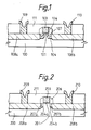
- Fig.1 shows, in section, a PLDD structure.
- It comprises a P-type silicon substrate 100, a gate insulating layer 101 formed on the top surface of the substrate 100, a gate 103 built on the gate insulating layer 101, an N-type source diffusion layer 108a, and an N-type drain diffusion layer 108b.
- the gate 103 has a surrounding wall 106, and the source and drain diffusion layers 108a and 108b have electrodes 109 and 110 respctively. These electrodes 109 and 110 are embedded in an overlying insulating layer 111.
- the drain diffusion layer is composed of an upper short projection 107 of least concentration of impurity such as arsenic, a surrounding section 104 of less concentration of impurity such as phosphorus, and an elongated section 108b of relatively high concentration of impurity such as arsenic, lying contiguous to the upper projection 107 and surrounding section 104, which end at a location under one edge of the gate 103.
- one object of the present invention is to provide an improved metal-oxide semiconductor field-effect transistor whose structure permits reduction of its size without lowering its current driving capability.
- a metal oxide-semiconductor field-effect transistor comprises: a semiconductor substrate of one conductivity type; a gate insulating layer formed on the top surface of said semiconductor substrate; a gate built on said gate insulating layer; and two diffused regions of the other conductivity type extending apart from under one and the other edge of said gate in the opposite directions, at least one of said diffused regions being composed of a first relatively short section of least concentration of impurity, a second relatively short section of less concentration of impurity, end a third relatively long section of relatively high concentration of impurity lying contiguous to each other and extending far from said gate in the order named, and being used as a drain diffusion layer whereas the other diffused region being used as a source diffusion layer.
- Another object of the present invention is to provide a method of making such an improved metal-oxide semiconductor field-effect transistor.
- a method of making a metal-oxide semiconductor field-effect transistor comprises the steps of: preparing a semi-fabricated product comprising a semiconductor substrate of one conductivity type with a gate insulating layer formed on its top surface, and a gate built on said gate insulating layer; injecting an impurity of the other conductivity type into said semiconductor substrate perpendicular to the top surface of said semiconductor substrate to form two opposite diffusion layers of least concentration of impurity in said semiconductor substrate, intending from first and second locations under one and the other edge of said gate respectively in the opposite directions; forming a side wall surrounding said gate on said semiconductor substrate; injecting the impurity of the other conductivity type into said semiconductor substrate at a given acute angle with respect to the normal line perpendicular to the top surface of said semiconductor substrate to form two opposite diffusion layers of less concentration of impurity in said semiconductor substrate, extending short of the terminal ends of said diffusion layers of least concentration of impurity; injecting the impurity of the other conductivity the into said semiconductor substrate perpendicular to the top surface of
- a method of making a metal-oxide semiconductor field-effect transistor comprises the steps of: preparing a semi-fabricated product comprising a semiconductor substrate of one conductivity type with a gate insulating layer formed on its top surface, and a gate built on said gate insulating layer; injecting an impurity of the other conductivity type into said semiconductor substrate perpendicular to the top surface of said semiconductor substrate to form two opposite diffusion layers of least concentration of impurity in said semiconductor substrate, extending from first and second locations under one and the other edge of said gate in the opposite directions; forming a first side wall surrounding said gate on said semiconductor substrate; injecting the impurity of the other conductivity type into said semiconductor substrate perpendicular to the top surface of said semiconductor substrate to form two opposite diffusion layers of less concentration of impurity in said semiconductor substrate, extending short of the terminal ends of said diffusion layers of least concentration of impurity; forming a second side wall surrounding said first side wall on said semiconductor substrate; injecting the impurity of the other conductivity type into said semiconductor substrate perpendicular
- an improved MOSFET according to one embodiment of the present invention is shown as comprising: a P-type silicon substrate 200; a gate insulating layer 201 of silicon formed on the top surface of the substrate 200; a gate 203 built on the gate insulation 201; an N-type source diffusion layer 204a and an N- type drain diffusion layer 204b extending toward and ending at a first location under one and the other edge of the gate 203 respectively in the opposite directions in the substrate 100; and an N-type source diffusion layer 207a and an N-type drain diffusion layer 207b extending toward and ending at a second location under one and the other edge of the gate 203 respectively in the oposite direction in the substrate 200.
- the source diffusion layer is composed of a first relatively short section 204a of least concentration of impurity (at most 2 x 1018 cm ⁇ 2), a second relatively short section 207a of less concentration of impurity (at most 1 x 1019 cm ⁇ 3 ), and a third relatively long section 208a of relatively high concentration of impurity (at least 2 x 1020 cm ⁇ 3) lying contiguous to each other and extending far from the first location in the order named.
- the drain diffusion layer has also the same structure.
- the first short section 204a and 204b of least concentration and the second short sections 207a and 207b of less concentration extend a same depth, thereby causing carriers to travel through an increased transverse area in the semiconductor substrate 200 compared with a PLDD structure, in which carriers come together close to the top surface of the semiconductor substrate 200.
- an improved MOSFET according to the present invention is guaranteed free of deterioration of the characteristics of the device.
- the parasitic resistor is reduced two to three times, and accordingly the current driving capability is increased.
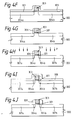
- FIGs.3A to 3J a method of making such a MOSFET according to the present invention is described.
- Figs.3A to 3D show how a semi-fabricated product comprising a semiconductor substrate of one conductivity type with a gate insulating layer formed on its top surface, and a gate built on the gate insulating layer can be prepared according to a conventional method.
- a P-type silicon substrate 200 is prepared (Fig.3A); a silicon oxide layer 201 is formed on the top surface of the substrate 200 by heating the substrate 200 in an oxidizing atomosphere (Fig.3B); a polysilicon layer 202 is formed on the silicon oxide layer 201 (Fig.3C); and the polysilicon layer 202 is subjected to anisotropic etching to leave a grate 203 on the silicon oxide layer 201 (Fig.3D).
- a semi-fabricated product results.
- Phosphorus ions ( 1 x 1013 cm ⁇ 2; 40 keV) is injected perpendicular to the top surface of the P-type substrate to form two opposite N-type diffusion layers 204a and 204b of least concentration of phosphorus in the substrate 200. These diffused regions 204a and 204b extend from first and second locations under one and the other edge of the gate 203 respectively in the opposite directions (Fig.3E).
- a 2000 angstrom-thick oxide layer 205 is formed on the semi-fabricated product (Fig.3F); and the thick oxide layer 205 is subjected to anisotropic etching until the top surface of the substrate 200 is exposed to leave a side wall 206 surrounding the gate 203 (Fig 3G).
- Phosphorus ions (5 x 1013 cm -Z ; 50 to 60 KeV) are injected to the P-type substrate 200 at 45 degrees to form two opposite N-type diffusion layers 207a and 207b of least concentration of phosphorus in the substrate 200 (Fig.3H). These diffused regions 207a and 207b extend short of the terminal ends of the diffusion layers 204a and 204b of least concentration of phosphorus.
- Arsenic ions (5 x 1013 cm ⁇ 2; 70 KeV) is injected to the P-type substrate 200 perpendicular to the top surface of the substrate to form two opposite diffusion layers 208a and 208b of relatively high concentration of arsenic in the substrate 200 (Fig.3I). These heavily diffused regions 208a and 208b extend from first and second locations under one and the other edge of the side wall 206 in the opposite directions.
- source electrode 209, drain electrode 210 and gate electrode are formed respectively (Fig.3J).
- two diffused regions 208a and 208b are of the same construction. Conveniently this permits either diffused region to be used as drain when the device is actually used.
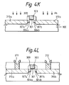
- a semi-fabricated product comprising a P-type substrate 300 with a gate insulating layer 301 of metal oxide formed on its top surface, and a gate 303 built on the gate insulating layer 301 is prepared according to a conventional method.
- Phosphorus ions (1 x 1013 cm ⁇ 2; 40 KeV) is injected perpendicular to the top surface of the P-type substrate 300 to form two opposite N-type diffusion layers 304a and 304b of least concentration of phosphorus in the substrate 300.
- These diffused regions 304a and 304b extend from first and second locations under one and the other edge of the gate 303 respectively in the opposite directions (Fig.3E).
- a 1000 angstrom-thick oxide layer 305 is formed on the semi-fabricated product (Fig.4F); and the thick oxide layer 305 is subjected to anisotropic etching until the top surface of the substrate 300 is exposed to leave a side wall 306 surrounding the gate 303 (Fig.4G).
- Phosphorus ions (5 x 1012 cm ⁇ 2; 40 KeV) are injected perpendicular to the P-type substrate 300 to form two opposite N-type diffusion layers 307a and 307b of least concentration of phosphorus in the substrate 300 (Fig.4H). These diffused regions 307a and 307b extend short of the terminal ends of the diffusion layers 304a and 304b of least concentration of phosphorus.
- FIG.4I Another 1000 angstrom-thick oxide layer 308 is formed on the sidewalled product (Fig.4I); and the tick oxide layer 308 is subjected to anisotropic etching until the top surface of the substrate 300 is exposed to leave a second side wall 309 surrounding the first side wall 306 of the gate 303 (Fig.4J).
- Arsenic ions (5 x 1015 cm ⁇ 2; 70 KeV) are injected perpendicular to the P-type substrate 300 to form two opposite diffusion layers 310a and 310b of relatively high concentration of arsenic in the substrate 300 (Fig.4K). These heavily diffused regions 301a and 310b extend from first and second locations under one and the other edge of the second side wall 309 in the opposite directions.
- source electrode 311, drain electrode 312 and gate electrode are formed respectively (Fig.4L).
- a metal oxide-semiconductor fieldeffect transistor thus made has two similar diffused regions each extending toward and ending at a location under one of the other edge of the gate 203 or 303 in the substrate 200 or 300. It is composed of a first relatively short section 204a 204b or 304a, 304b of least concentration of impurity, a second relatively short section 207a, 207b or 307a, 307b of less concentration of impurity, and a third relatively long section 208a, 208b or 310a, 310b of relatively high concentration of impurity. As described earlier, this permits either diffused region to be used as drain when actually the device is used.
Landscapes
- Insulated Gate Type Field-Effect Transistor (AREA)
Applications Claiming Priority (2)
| Application Number | Priority Date | Filing Date | Title |
|---|---|---|---|
| JP339394/90 | 1990-11-30 | ||
| JP2339394A JPH04206933A (ja) | 1990-11-30 | 1990-11-30 | 半導体装置 |
Publications (2)
| Publication Number | Publication Date |
|---|---|
| EP0489559A1 true EP0489559A1 (fr) | 1992-06-10 |
| EP0489559B1 EP0489559B1 (fr) | 1995-07-12 |
Family
ID=18327060
Family Applications (1)
| Application Number | Title | Priority Date | Filing Date |
|---|---|---|---|
| EP91311183A Expired - Lifetime EP0489559B1 (fr) | 1990-11-30 | 1991-12-02 | Transistor à effet de champ métal-oxyde semi-conducteur LDD et sa méthode de fabrication |
Country Status (4)
| Country | Link |
|---|---|
| US (1) | US5292674A (fr) |
| EP (1) | EP0489559B1 (fr) |
| JP (1) | JPH04206933A (fr) |
| DE (1) | DE69111203T2 (fr) |
Cited By (1)
| Publication number | Priority date | Publication date | Assignee | Title |
|---|---|---|---|---|
| WO1998032176A1 (fr) * | 1997-01-21 | 1998-07-23 | Advanced Micro Devices, Inc. | JONCTION A ZONES nLDD HYBRIDES As/P AVEC FONCTIONNEMENT A TENSION D'ALIMENTATION MOYENNE POUR MICROPROCESSEURS A GRANDE VITESSE |
Families Citing this family (6)
| Publication number | Priority date | Publication date | Assignee | Title |
|---|---|---|---|---|
| US5376566A (en) * | 1993-11-12 | 1994-12-27 | Micron Semiconductor, Inc. | N-channel field effect transistor having an oblique arsenic implant for lowered series resistance |
| US5439835A (en) * | 1993-11-12 | 1995-08-08 | Micron Semiconductor, Inc. | Process for DRAM incorporating a high-energy, oblique P-type implant for both field isolation and punchthrough |
| US5614432A (en) * | 1994-04-23 | 1997-03-25 | Nec Corporation | Method for manufacturing LDD type MIS device |
| US5478763A (en) * | 1995-01-19 | 1995-12-26 | United Microelectronics Corporation | High performance field effect transistor and method of manufacture thereof |
| US5935867A (en) * | 1995-06-07 | 1999-08-10 | Advanced Micro Devices, Inc. | Shallow drain extension formation by angled implantation |
| US6180470B1 (en) * | 1996-12-19 | 2001-01-30 | Lsi Logic Corporation | FETs having lightly doped drain regions that are shaped with counter and noncounter dorant elements |
Citations (3)
| Publication number | Priority date | Publication date | Assignee | Title |
|---|---|---|---|---|
| EP0187016A2 (fr) * | 1984-12-27 | 1986-07-09 | Kabushiki Kaisha Toshiba | Transistor à effet de champ métal isolateur-semi-conducteur à drain faiblement dopé et procédé pour sa fabrication |
| US4746624A (en) * | 1986-10-31 | 1988-05-24 | Hewlett-Packard Company | Method for making an LDD MOSFET with a shifted buried layer and a blocking region |
| US4771012A (en) * | 1986-06-13 | 1988-09-13 | Matsushita Electric Industrial Co., Ltd. | Method of making symmetrically controlled implanted regions using rotational angle of the substrate |
Family Cites Families (12)
| Publication number | Priority date | Publication date | Assignee | Title |
|---|---|---|---|---|
| JPS60136376A (ja) * | 1983-12-26 | 1985-07-19 | Hitachi Ltd | 半導体装置の製造方法 |
| JPS61216364A (ja) * | 1985-03-20 | 1986-09-26 | Fujitsu Ltd | 半導体装置 |
| JPS62113474A (ja) * | 1985-11-13 | 1987-05-25 | Toshiba Corp | 半導体集積回路の製造方法 |
| JPH0789587B2 (ja) * | 1985-12-27 | 1995-09-27 | 株式会社東芝 | 絶縁ゲート型電界効果トランジスタおよびその製造方法 |
| US4835740A (en) * | 1986-12-26 | 1989-05-30 | Kabushiki Kaisha Toshiba | Floating gate type semiconductor memory device |
| US5061975A (en) * | 1988-02-19 | 1991-10-29 | Mitsubishi Denki Kabushiki Kaisha | MOS type field effect transistor having LDD structure |
| JP2562688B2 (ja) * | 1989-05-12 | 1996-12-11 | 三洋電機株式会社 | 半導体装置の製造方法 |
| US5158903A (en) * | 1989-11-01 | 1992-10-27 | Matsushita Electric Industrial Co., Ltd. | Method for producing a field-effect type semiconductor device |
| US5023190A (en) * | 1990-08-03 | 1991-06-11 | Micron Technology, Inc. | CMOS processes |
| US5091763A (en) * | 1990-12-19 | 1992-02-25 | Intel Corporation | Self-aligned overlap MOSFET and method of fabrication |
| US5102815A (en) * | 1990-12-19 | 1992-04-07 | Intel Corporation | Method of fabricating a composite inverse T-gate metal oxide semiconductor device |
| US5162884A (en) * | 1991-03-27 | 1992-11-10 | Sgs-Thomson Microelectronics, Inc. | Insulated gate field-effect transistor with gate-drain overlap and method of making the same |
-
1990
- 1990-11-30 JP JP2339394A patent/JPH04206933A/ja active Pending
-
1991
- 1991-11-29 US US07/800,170 patent/US5292674A/en not_active Expired - Fee Related
- 1991-12-02 EP EP91311183A patent/EP0489559B1/fr not_active Expired - Lifetime
- 1991-12-02 DE DE69111203T patent/DE69111203T2/de not_active Expired - Fee Related
Patent Citations (3)
| Publication number | Priority date | Publication date | Assignee | Title |
|---|---|---|---|---|
| EP0187016A2 (fr) * | 1984-12-27 | 1986-07-09 | Kabushiki Kaisha Toshiba | Transistor à effet de champ métal isolateur-semi-conducteur à drain faiblement dopé et procédé pour sa fabrication |
| US4771012A (en) * | 1986-06-13 | 1988-09-13 | Matsushita Electric Industrial Co., Ltd. | Method of making symmetrically controlled implanted regions using rotational angle of the substrate |
| US4746624A (en) * | 1986-10-31 | 1988-05-24 | Hewlett-Packard Company | Method for making an LDD MOSFET with a shifted buried layer and a blocking region |
Non-Patent Citations (2)
| Title |
|---|
| INTERNATIONAL ELECTRON DEVICES MEETING 1980 TECHNICAL DIGEST pages 764 - 767; W. R. HUNTER ET AL: 'NEW EDGE-DEFINED VERTICAL-ETCH APPROCHES FOR SUBMICROMITER MOSFET FABRICATION' * |
| PATENT ABSTRACTS OF JAPAN vol. 9, no. 298 (E-361)(2021) 26 November 1985 & JP-A-60 136 376 ( HITACHI SEISAKUSHO K.K. ) 19 July 1985 * |
Cited By (1)
| Publication number | Priority date | Publication date | Assignee | Title |
|---|---|---|---|---|
| WO1998032176A1 (fr) * | 1997-01-21 | 1998-07-23 | Advanced Micro Devices, Inc. | JONCTION A ZONES nLDD HYBRIDES As/P AVEC FONCTIONNEMENT A TENSION D'ALIMENTATION MOYENNE POUR MICROPROCESSEURS A GRANDE VITESSE |
Also Published As
| Publication number | Publication date |
|---|---|
| JPH04206933A (ja) | 1992-07-28 |
| DE69111203D1 (de) | 1995-08-17 |
| EP0489559B1 (fr) | 1995-07-12 |
| US5292674A (en) | 1994-03-08 |
| DE69111203T2 (de) | 1996-04-04 |
Similar Documents
| Publication | Publication Date | Title |
|---|---|---|
| US6825531B1 (en) | Lateral DMOS transistor with a self-aligned drain region | |
| US5918137A (en) | MOS transistor with shield coplanar with gate electrode | |
| US6207519B1 (en) | Method of making semiconductor device having double spacer | |
| EP0336393B1 (fr) | Dispositif semi-conducteur dont la structure rend difficile l'opération du transistor parasite et méthode de fabrication | |
| US5016067A (en) | Vertical MOS transistor | |
| US6924529B2 (en) | MOS transistor having a recessed gate electrode and fabrication method thereof | |
| US5798549A (en) | Conductive layer overlaid self-aligned MOS-gated semiconductor devices | |
| KR910002037B1 (ko) | 반도체장치 및 그 제조방법 | |
| US4929991A (en) | Rugged lateral DMOS transistor structure | |
| US6238985B1 (en) | Semiconductor device and method for fabricating the same | |
| US5291049A (en) | Mosfet with buried element isolation regions | |
| US6362060B2 (en) | Method for forming semiconductor device having a gate in the trench | |
| EP0489559A1 (fr) | Transistor à effet de champ métal-oxyde semi-conducteur LDD et sa méthode de fabrication | |
| US5451536A (en) | Power MOSFET transistor | |
| JPH03109775A (ja) | 絶縁ゲート型半導体装置 | |
| JP2849199B2 (ja) | 半導体装置の製造方法 | |
| JPH06224216A (ja) | トランジスター及びその製造方法 | |
| JPH0789587B2 (ja) | 絶縁ゲート型電界効果トランジスタおよびその製造方法 | |
| KR0175367B1 (ko) | 반도체 장치 및 그 제조 방법 | |
| US5422509A (en) | Integrated current-limiter device for power MOS transistors | |
| US6215153B1 (en) | MOSFET and method for fabricating the same | |
| JP2727590B2 (ja) | Mis型半導体装置 | |
| JP3625603B2 (ja) | Dmos構造を有する半導体装置およびその製造方法 | |
| JPH0555583A (ja) | 絶縁ゲート型バイポーラトランジスタの製造方法 | |
| JP3061157B2 (ja) | 半導体素子の形成方法 |
Legal Events
| Date | Code | Title | Description |
|---|---|---|---|
| PUAI | Public reference made under article 153(3) epc to a published international application that has entered the european phase |
Free format text: ORIGINAL CODE: 0009012 |
|
| 17P | Request for examination filed |
Effective date: 19911217 |
|
| AK | Designated contracting states |
Kind code of ref document: A1 Designated state(s): DE FR GB |
|
| 17Q | First examination report despatched |
Effective date: 19940214 |
|
| GRAA | (expected) grant |
Free format text: ORIGINAL CODE: 0009210 |
|
| AK | Designated contracting states |
Kind code of ref document: B1 Designated state(s): DE FR GB |
|
| REF | Corresponds to: |
Ref document number: 69111203 Country of ref document: DE Date of ref document: 19950817 |
|
| ET | Fr: translation filed | ||
| PGFP | Annual fee paid to national office [announced via postgrant information from national office to epo] |
Ref country code: GB Payment date: 19951130 Year of fee payment: 5 |
|
| PGFP | Annual fee paid to national office [announced via postgrant information from national office to epo] |
Ref country code: FR Payment date: 19951218 Year of fee payment: 5 |
|
| PGFP | Annual fee paid to national office [announced via postgrant information from national office to epo] |
Ref country code: DE Payment date: 19960228 Year of fee payment: 5 |
|
| PLBE | No opposition filed within time limit |
Free format text: ORIGINAL CODE: 0009261 |
|
| STAA | Information on the status of an ep patent application or granted ep patent |
Free format text: STATUS: NO OPPOSITION FILED WITHIN TIME LIMIT |
|
| 26N | No opposition filed | ||
| PG25 | Lapsed in a contracting state [announced via postgrant information from national office to epo] |
Ref country code: GB Effective date: 19961202 |
|
| GBPC | Gb: european patent ceased through non-payment of renewal fee |
Effective date: 19961202 |
|
| PG25 | Lapsed in a contracting state [announced via postgrant information from national office to epo] |
Ref country code: FR Effective date: 19970829 |
|
| PG25 | Lapsed in a contracting state [announced via postgrant information from national office to epo] |
Ref country code: DE Effective date: 19970902 |
|
| REG | Reference to a national code |
Ref country code: FR Ref legal event code: ST |