EP0491290A2 - Tester für integrierte Schaltungen - Google Patents
Tester für integrierte Schaltungen Download PDFInfo
- Publication number
- EP0491290A2 EP0491290A2 EP91121372A EP91121372A EP0491290A2 EP 0491290 A2 EP0491290 A2 EP 0491290A2 EP 91121372 A EP91121372 A EP 91121372A EP 91121372 A EP91121372 A EP 91121372A EP 0491290 A2 EP0491290 A2 EP 0491290A2
- Authority
- EP
- European Patent Office
- Prior art keywords
- memory
- pattern
- channels
- test
- test pattern
- Prior art date
- Legal status (The legal status is an assumption and is not a legal conclusion. Google has not performed a legal analysis and makes no representation as to the accuracy of the status listed.)
- Granted
Links
Images




Classifications
-
- G—PHYSICS
- G01—MEASURING; TESTING
- G01R—MEASURING ELECTRIC VARIABLES; MEASURING MAGNETIC VARIABLES
- G01R31/00—Arrangements for testing electric properties; Arrangements for locating electric faults; Arrangements for electrical testing characterised by what is being tested not provided for elsewhere
- G01R31/28—Testing of electronic circuits, e.g. by signal tracer
-
- G—PHYSICS
- G11—INFORMATION STORAGE
- G11C—STATIC STORES
- G11C29/00—Checking stores for correct operation ; Subsequent repair; Testing stores during standby or offline operation
- G11C29/56—External testing equipment for static stores, e.g. automatic test equipment [ATE]; Interfaces therefor
-
- G—PHYSICS
- G01—MEASURING; TESTING
- G01R—MEASURING ELECTRIC VARIABLES; MEASURING MAGNETIC VARIABLES
- G01R31/00—Arrangements for testing electric properties; Arrangements for locating electric faults; Arrangements for electrical testing characterised by what is being tested not provided for elsewhere
- G01R31/28—Testing of electronic circuits, e.g. by signal tracer
- G01R31/317—Testing of digital circuits
- G01R31/3181—Functional testing
- G01R31/319—Tester hardware, i.e. output processing circuits
- G01R31/31903—Tester hardware, i.e. output processing circuits tester configuration
- G01R31/31908—Tester set-up, e.g. configuring the tester to the device under test [DUT], down loading test patterns
-
- G—PHYSICS
- G01—MEASURING; TESTING
- G01R—MEASURING ELECTRIC VARIABLES; MEASURING MAGNETIC VARIABLES
- G01R31/00—Arrangements for testing electric properties; Arrangements for locating electric faults; Arrangements for electrical testing characterised by what is being tested not provided for elsewhere
- G01R31/28—Testing of electronic circuits, e.g. by signal tracer
- G01R31/317—Testing of digital circuits
- G01R31/3181—Functional testing
- G01R31/319—Tester hardware, i.e. output processing circuits
- G01R31/31917—Stimuli generation or application of test patterns to the device under test [DUT]
- G01R31/31919—Storing and outputting test patterns
-
- G—PHYSICS
- G01—MEASURING; TESTING
- G01R—MEASURING ELECTRIC VARIABLES; MEASURING MAGNETIC VARIABLES
- G01R31/00—Arrangements for testing electric properties; Arrangements for locating electric faults; Arrangements for electrical testing characterised by what is being tested not provided for elsewhere
- G01R31/28—Testing of electronic circuits, e.g. by signal tracer
- G01R31/317—Testing of digital circuits
- G01R31/3181—Functional testing
- G01R31/319—Tester hardware, i.e. output processing circuits
- G01R31/31917—Stimuli generation or application of test patterns to the device under test [DUT]
- G01R31/31926—Routing signals to or from the device under test [DUT], e.g. switch matrix, pin multiplexing
Definitions
- the present invention relates to an IC tester for testing a memory incorporated in a logical IC device.
- Some of logical IC's have incorporated therein a memory.
- terminals leading to the memory can be all connected to external pins by switching the mode of operation. Accordingly, the incorporated memory can be tested independently of the logical circuits by setting the mode.
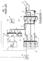
- Fig. 1 shows the construction of a conventional IC tester for testing IC's of this kind.
- the IC tester is provided with a logic test pattern generator 10 for generating logic test patterns for testing a logical circuit and a memory test pattern generator 20 for generating memory test patterns for testing a memory.
- the IC tester is adapted to be switchable between a logical circuit test mode and a memory test mode so as to test the logical circuit and the memory independently of each other.
- the logic test pattern generator 10 comprises a logic test pattern memory 10A, a waveform control pattern memory 10B and a logical comparison control pattern memory 10C.
- Logic pattern data PLA, waveform control pattern data PB and comparison control pattern data PC which are output from the logic test pattern memory 10A, the waveform control pattern memory 10B and the logical comparison control pattern memory 10C, are provided to a waveform formatter 31, a waveform controller 32 and a logical comparison part 33, respectively.
- the waveform formatter 31 generates a logical waveform, based on the logic test pattern data PLA read out of the logic test pattern memory 10A and provided via an OR circuit 61 and a timing signal TS provided from a timing generator 40.
- the logical waveform is supplied as a logic test pattern signal to an IC under test 36 via a driver group 35.
- the waveform control pattern data PB read out of the waveform control pattern memory 10B is input into the waveform controller 32 to effect ON-OFF control of each driver of the driver group 35. That is, when a test pattern is applied to a terminal pin of the IC under test 36, the corresponding driver is controlled to enter the ON state (i.e. the activated state) and when a response signal is taken out of the IC 36, the driver is controlled to enter the OFF state (i.e. the state of a high output impedance).
- the comparison control pattern data PC read out of the logical comparison control pattern memory 10C is input into the logical comparison part 33, wherein it is controlled on a bitwise basis (i.e. for each pin) whether or not to make a comparison between the logic of the response output signal from the IC under test 36, decided by a logic decision comparator group 37, and expected value pattern PD derived from the logic test pattern data PLA.
- Reference numeral 38 denotes a failure analysis memory for storing the results of logical comparison from the logical comparison part 33.
- the timing generator 40 applies the timing signal TS to the waveform formatter 31, the waveform controller 32 and the logical comparison part 33 to time their operations.
- the timing generator 40 also applies an operating clock CK to a sequence controller 50. Based on the operating clock CK supplied from the timing generator 40, the sequence controller 50 generates a control signal such as a pattern address, which is applied to the test pattern memory 10A, the waveform control pattern memory 10B and the logical comparison control pattern memory 10C to control their readout sequences to read out therefrom the respective pieces of pattern data PLA, PB and PC.
- the control signal such as a pattern address, provided from the sequence controller 50, is used to read out the waveform control pattern data PB and the comparison control pattern data PC from the logic test pattern generator 10 and, in this instance, the logic test pattern data PLA is not read out, but instead memory test pattern data PMA is read out of the memory test pattern generator 20 by the same control signal.
- the memory test pattern data PMA is composed of address pattern data which is applied to the address input pins of the IC under test 36, input data pattern data which is provided to the data input pins of the IC 36 and control pattern data which controls whether to effect a write or read in each test cycle. These pieces of data are respectively provided at predetermined ones of output terminals Q0 to Q i of the memory test pattern generator 20 irrespective of the pin array of the IC under test 36.
- the memory test pattern data PMA is selected by a pattern selector 25, for each pin, in accordance with terminal select addresses set in a pattern select register 26 and is provided via the OR circuit 61 to the waveform formatter 31.
- the pattern selector 25 is made up of multiplexers MP1 to MP n provided corresponding to pins T1 to T n of the IC under test 36 and each having connected thereto all the output terminals Q0 to Q i of the memory test pattern generator 20.
- the pattern select register 26 is made up of terminal address registers R1 to R n connected to control terminals C of the multiplexers MP1 to MP n , respectively.
- each of the terminal address registers R1 to R n Prior to the test of the IC 36 an address is set in each of the terminal address registers R1 to R n for specifying any one of the output terminals Q1 to Q i which is to be selected by each of the multiplexers MP1 to MP n in accordance with the pin array of the IC 36.
- selected pieces of the address pattern data and the input data pattern data are provided to the address and input pins of the IC under test 36 according to the setting of the pattern select register 26.
- the sequence controller 50 provides to an inhibit terminal INH of the pattern selector 25 a control signal GS which represents whether the test currently under way is a logic test or memory test.
- the control signal GS is, for example, a "1" representing a logic test
- the pattern selector 25 inhibits its all outputs, preventing erroneous outputting of signals from the memory test pattern generator 20.
- the memory test pattern data PMA selected by the pattern selector 25 for each pin is provided to the waveform formatter 31, and at the same time, the waveform control pattern data PB and the comparison control pattern data PC are provided to the waveform controller 32 and the logical comparison part 33 from the logic test pattern generator 10, effecting waveform control and control of the logical comparison.
- the waveform control and the logical comparison must be conducted for each pin, and consequently, when the positions of pins for testing a memory differ with the types of IC's to be tested, it is necessary that programs for generating the waveform control pattern data PB and the comparison control pattern data PC be prepared for each type.
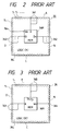
- Figs. 2 through 4 some memory built-in type logic IC devices have such arrangements of terminals as shown in Figs. 2 through 4.
- IC 36 depicted in Fig. 2 there are arranged memory test address input pins 361 on a side A containing a first pin T1, memory test data output pins 362 on a side B, and memory test data input pins 363 and a read/write control signal input pin 364 on a side D containing a last pin T n .
- These pins 361 through 364 are connected to a memory 36M incorporated in the IC 36.
- the other remaining pins are those for a logic circuit 36L shown as an area except the memory 36M in the IC 36.
- the IC depicted in Fig. 3 has memory test data I/O pins 365 arranged on the side A containing the first pin T1, the read/write control signal input pin 364 on the side B and the memory test address input pins 361 on the side D.
- the IC 36 shown in Fig. 4 has built therein two memories 36M1 and 36M2.
- the address input pins 361 of the memory 36M1 and the data I/O pins 365 of the memory 36M2 on the side A there are arranged the address input pins 361 of the memory 36M1 and the data I/O pins 365 of the memory 36M2 on the side A, the data output pins 362 of the memory 36M1 and the read/write control signal input pin 364 of the memory 36M2 on the side B and the data input pins 363 and the read/write control signal input pin 364 of the memory 36M1 and the address input pins 361 of the memory 36M2 on the side D.
- the memory test pattern generator includes a memory test pattern generation part, a waveform control pattern data memory part and a logical comparison control pattern memory part.
- Memory test pattern data, waveform control pattern data and logical comparison control data from the memory test pattern generation part, the waveform control pattern data memory part and the logical comparison control pattern memory part are respectively selected by pattern selectors for each pin and provided to the waveform formatter, the waveform controller and the logical comparison part.
- the waveform control pattern data and the logical comparison control pattern data can be selected by the pattern selectors for each pin and then output, programs for the generation of the memory test pattern data, the waveform control pattern data and the logical comparison control pattern data in the memory test pattern generator can be produced independently of the arrangement of pins of the IC under test. Consequently, programs for the generation of pattern data in the memory test pattern generator need not be prepared for each type of the IC to be tested. This affords reduction of the capacities of the memories forming the logic test pattern generator.
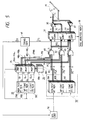
- Fig. 5 illustrates in block form an embodiment of the present invention.
- this embodiment includes the logic test pattern generator 10, the memory test pattern generator 20, the pattern selector 25, the pattern select register 26, the waveform formatter 31, the waveform controller 32, the logical comparison part 33, the driver group 35, the IC under test 36, the logic decision comparator group 37, the timing generator 40 and the sequence controller 50.
- These pieces of data PMA, PB, PC and PLA are each output over n channels in anticipation of an IC which is assumed to have the largest number n of pins among IC's to be tested.
- the driver group 35 includes n drivers accordingly and the logic decision comparator group 37 is also made up of n comparators. All the other constituent elements 25, 26, 31, 32, 33, 61, 62 and 63 are also provided in units of n channels. The constituent elements are interconnected via n channel lines.
- the memory test pattern generator 20 comprises a memory test pattern generation part 20A, a waveform control pattern memory 20B and a logical comparison control pattern memory 20C.
- the memory test pattern generation part 20A generates the memory test pattern data PMA composed of address and data patterns to be provided to the IC under test, and the waveform control pattern data PB and the comparison control pattern data PC are read out of the waveform control pattern memory 20B and the logical comparison control pattern memory 20C, respectively.
- These pieces of data PMA, PB and PC are provided at output terminals Q0 to Q i , Q i+1 to Q j and Q j+1 to Q k , respectively.
- the multiplexer MA h has connected to its input all the output terminals Q0 to Q i of the memory test pattern generation part 20A
- the multiplexer MB h has connected to its input all the output terminals Q i+1 to Q j of the waveform control pattern memory 20B
- the multiplexer MC h has connected to its input all the output terminals Q j+1 to Q k of the logical comparison control pattern memory 20C.
- the pattern select register 26 is formed by a register group including three registers RA h , RB h and RC h for each channel.
- terminal select addresses SAah, SAbh and SAch are set for selectively connecting one of the terminals Q0 to Q i , one of the terminals Q i+1 to Q j and one of the terminals Q j+1 to Q k to the multiplexers MA h , MB h and MC h corresponding to the registers RA h , RB h and RC h , respectively.
- the terminal select addresses are provided as terminal select control signals to the multiplexers MA h , MB h and MC h .
- the waveform control pattern data PB and the comparison control pattern data PC are output from the memory test pattern generation part 20A, the waveform control pattern memory 20B and the logical comparison pattern memory 20C, respectively.
- These pieces of data PMA, PB and PC are selected by the pattern selector 25 for each channel in accordance with the terminal select addresses SAah, SAbh and SAch set in the pattern select register 26, and the memory test pattern data PMA thus selected for each channel is input into the waveform formatter 31 via the OR circuit 61.
- the memory test pattern data PMA and the timing signal TS from the timing generator 40 are used to produce a memory test pattern signal in an actual waveform as in the prior art, and the memory test pattern signal is applied via the driver group 35 to the corresponding channel of the IC under test 36.
- the waveform control pattern data PB and the comparison control pattern data PC are sorted by the pattern selector 25 for each pin and are supplied to the waveform controller 32 and the logical comparison part 33 in the channel corresponding to the desired pin.
- the waveform control pattern memory 20B and the logical comparison control pattern memory 20C of the memory test pattern generator 20 may be small in capacity.
- the waveform control pattern data PB and the logical comparison control pattern data PC for executing the memory test need not be stored in the logic test pattern generator 10, the capacities of the waveform control pattern memory 10B and the logical comparison control pattern memory 10C can be reduced substantially.
- Fig. 6 illustrates a modified form of the present invention.
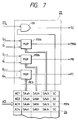
- the pattern select register 26 in the Fig. 5 embodiment is substituted with a pattern select memory 261 and an address AD is produced by the sequence controller 50 and is used to access the pattern select memory 261 to read out therefrom three terminal select addresses for each channel, by which the selective connections of the multiplexers MA h , MB h and MC h of the pattern selector 25 are controlled.
- the pattern select memory 261 has n memory planes MP1 to MP n which are accessed by the common address AD. As seen from Fig.
- the terminal select state of the pattern selector 25 can be switched in a desired step in the test sequence.
- the two memories 36M1 and 36M2 of different pin arrangements, built in the IC as shown in Fig. 4, can be tested successively at high speed.
- the IC 36 may sometimes have a construction in which the address and data are alternately input into the memory 36M via a common input pins and are latched in a memory address latch and a memory data data latch alternately with each other. Also in such a case, according to the Fig. 6 embodiment, the pin connection can be switched as required during the generation of a test pattern. In some cases, the IC 36 may have a construction in which only one input pin is provided for each of the address and the data to be supplied to the memory 36M and the address and data are input serially into an address register and a data register, respectively.
- parallel addresses and parallel data are respectively converted into serial form by sequentially changing the selective terminal connection in the pattern selector 25 and are each provided to one channel lines corresponding to each of the address input pin and the data input pin. This can be done by sequentially switching those of the inputs to the multiplexers of the two channels which correspond to the parallel addresses and the parallel data.
- the pieces of pattern data PLA, PB and PC from the logic test pattern generator 10 and the pieces of pattern data PMA, PB and PC from the memory test pattern generator 20 are switched by switching circuits 601, 602 and 603 for each channel in response to a switching control signal SC and then provided to the waveform formatter 31, the waveform controller 32 and the logical comparison part 33.
- the control signal GS from the sequence controller 50 is applied to all of n gates G1 to G n provided in the pattern selector 25 to enable and disable them during the memory test and during the logic test.
- the switching control data SC for switching control of the switching circuits 601, 602 and 603 for each channel as well as the terminal select addresses SAah, SAbh and SAch.
- the switching data SC read out of the pattern select memory 261 is provided to the switching circuits 601, 602 and 603 via the gates G1 to G n which are enabled only during the memory test.
- the outputs SC of the gates G1 to G n are, for example, all "0's,” by which all the channels of the switching circuits 601, 602 and 603 are connected to the side of the logic test pattern generator 10.
- the channels corresponding to the switching circuits 601, 602 and 603 are connected to the logic test pattern generator 10 or memory test pattern generator 20, depending on whether the switching control data SC set in each of the memory planes MP1 to MP n is a "0" or "1.”
- Fig. 8 illustrates a modified form of the Fig. 5 embodiment.
- the sequence controller 50 in Fig. 5 is made up of a main sequence control part 50A which operates in accordance with the common operating clock CK from the timing generator 40 and a memory test pattern sequence control part 50B.
- the logic part and the memory part are each tested after completion of the test of either one of them.
- the memory test is conducted for each area of the memory and consequently for each sequence of patterns and the logic test is also conducted for each sequence of patterns; in this case, the memory test and the logic test for each sequence of patterns are made alternately with each other.
- the test sequence is placed under control of the sequence controller.
- the main sequence control part 50A applies a start signal SS to the memory test pattern sequence control part 50B upon completion of the test of the logical circuit part (not shown) of the IC by a series of patterns.
- the memory test pattern sequence control part 50B responds to the start signal SS to execute a program portion for generating a series of memory test patterns, by which the memory test pattern generator 20 is controlled to make the memory test by the series of patterns.
- the memory test pattern sequence control part 50B Upon completion of the execution of the program portion for generating the series of patterns, the memory test pattern sequence control part 50B applies an end signal ES to the main sequence control part 50A and stops the execution of the memory test pattern generation program.
- the main sequence control part 50A executes again the program portion for generating a series of logic test patterns for the logic test. Thereafter, the logic test and the memory test are repeated using the same procedure until all the necessary tests of the IC are completed.
- the logic test pattern generation program for the main sequence control part 50A may be created taking into account only the step in which to conduct the memory test and the contents of the memory test to be conducted in the step need not be taken into consideration.
- the memory test pattern generation program for the memory test pattern sequence control part 50B may be created taking into account only the contents of the memory test to be conducted. This allows ease in the production of the pattern generation programs for the IC test.
- the logic test pattern generator 10 can be operated by a different sequence, it is possible to operate the logical circuit of the IC under test simultaneously with its memory to test the influence of the former on the latter and to test an IC of a construction in which no memory test can be conducted unless a signal is applied to the pin for logical circuit use in a certain sequence.
- Fig. 9 illustrates another embodiment of the present invention in which a further modification of the main sequence control part 50A in Fig. 8 is applied to the embodiment of Fig. 6.
- the main sequence control part 50A comprises a logic test pattern sequence control part 50AA and a link control part 50C connected thereto.
- the link control part 50C is also connected to the memory test pattern sequence control part 50B.
- the link control part 50C applies the pattern generation start signal SS to the sequence control parts 50AA and 50B in a predetermined order and, at the same time, supplies the pattern selector 25 with the control signal GS which represents whether the memory test or logic test is to be conducted.
- the sequence control parts 50AA and 50B each execute a program portion for generating a series of patterns and, upon completion of the pattern generation, apply the end signal ES to the link control part 50C.
- the pattern generation program for the logic test pattern sequence control part 50AA can be produced without regard to the memory test.
- a sequence control program for the link control part 50C defines only the order of steps for conducting the memory test and the logic test in a series of test sequence, and hence the program can be created with more ease.
- the ON/OFF state of the driver 35 is not changed for each test cycle in a series of tests. That is, there is no need of generating waveform control pattern data by use of the logic test pattern generator 10 and the memory test pattern generator 20 but instead fixed n-bit data for specifying the ON/OFF state of each driver 35 corresponding to the type of the IC 36 is set in a register (not shown) provided in the waveform controller 32, and during the test of the IC 36 the n-bit data is provided to a control terminal of the driver 35 to fixedly control its ON/OFF state.
- the waveform control pattern memory 10B and the logical comparison pattern memory 10C in the logic test pattern generator 10 are required to store only the pattern generation program for the logic test and a program for generating patterns which are provided to pins for exclusive use of the logic circuit during the memory test -- this affords reduction of the capacities of memories forming the waveform control pattern memory 10B and the logical comparison control pattern memory 10C.
- the present invention employs the construction in which the selection of pins is controlled by the pattern selector 25, a set of test patterns needs only to be stored in the waveform control pattern memory 20B and the logical comparison control pattern memory 20C of the memory test pattern generator 20 independently of the pin arrangement of the IC under test.
- the waveform control pattern memory 20B and the logical comparison control pattern memory 20B can be formed by small-capacity memories.
Landscapes
- Engineering & Computer Science (AREA)
- General Engineering & Computer Science (AREA)
- Physics & Mathematics (AREA)
- General Physics & Mathematics (AREA)
- Tests Of Electronic Circuits (AREA)
Applications Claiming Priority (2)
| Application Number | Priority Date | Filing Date | Title |
|---|---|---|---|
| JP403627/90 | 1990-12-19 | ||
| JP2403627A JPH04218785A (ja) | 1990-12-19 | 1990-12-19 | Ic試験装置 |
Publications (3)
| Publication Number | Publication Date |
|---|---|
| EP0491290A2 true EP0491290A2 (de) | 1992-06-24 |
| EP0491290A3 EP0491290A3 (en) | 1992-10-28 |
| EP0491290B1 EP0491290B1 (de) | 1997-07-30 |
Family
ID=18513357
Family Applications (1)
| Application Number | Title | Priority Date | Filing Date |
|---|---|---|---|
| EP91121372A Expired - Lifetime EP0491290B1 (de) | 1990-12-19 | 1991-12-12 | Tester für integrierte Schaltungen |
Country Status (5)
| Country | Link |
|---|---|
| US (1) | US5432797A (de) |
| EP (1) | EP0491290B1 (de) |
| JP (1) | JPH04218785A (de) |
| KR (1) | KR960004439B1 (de) |
| DE (1) | DE69127060T2 (de) |
Cited By (5)
| Publication number | Priority date | Publication date | Assignee | Title |
|---|---|---|---|---|
| DE4433512C2 (de) * | 1993-09-21 | 2001-03-22 | Advantest Corp | Wellenform-Formatierungseinrichtung |
| DE19937820C2 (de) * | 1998-08-11 | 2002-07-04 | Advantest Corp | Vorrichtung zum Testen integrierter Halbleiterschaltungen und Verfahren zum Steuern derselben |
| EP1025479A4 (de) * | 1997-10-29 | 2004-09-08 | Credence Systems Corp | Parallelverarbeitendes mustergenerierverfahren für einen integrierten kreislauftester |
| CN101568845B (zh) * | 2006-12-22 | 2012-03-14 | 惠瑞捷(新加坡)私人有限公司 | 用于对待测设备进行测试的测试器、方法和计算机程序 |
| CN107547149A (zh) * | 2016-06-27 | 2018-01-05 | 中兴通讯股份有限公司 | 射频测试芯片 |
Families Citing this family (44)
| Publication number | Priority date | Publication date | Assignee | Title |
|---|---|---|---|---|
| JP3202439B2 (ja) * | 1993-10-07 | 2001-08-27 | 富士通株式会社 | 出力装置のテスト装置 |
| JPH07280883A (ja) * | 1994-04-04 | 1995-10-27 | Advantest Corp | 半導体試験装置 |
| US5673271A (en) * | 1994-08-19 | 1997-09-30 | Advantest Corporation | High speed pattern generator |
| JP3237473B2 (ja) * | 1995-06-29 | 2001-12-10 | 安藤電気株式会社 | マスク制御装置 |
| US5627478A (en) | 1995-07-06 | 1997-05-06 | Micron Technology, Inc. | Apparatus for disabling and re-enabling access to IC test functions |
| DE19680782C2 (de) * | 1995-07-26 | 2002-11-21 | Advantest Corp | Hochgeschwindigkeits- Mustergenerierungsverfahren und unter Verwendung dieses Verfahrens arbeitender Hochgeschwindigkeits-Mustergenerator |
| JP3150611B2 (ja) * | 1996-03-29 | 2001-03-26 | 株式会社東芝 | パターン発生装置 |
| JPH09288153A (ja) * | 1996-04-19 | 1997-11-04 | Advantest Corp | 半導体試験装置 |
| US5677913A (en) * | 1996-07-01 | 1997-10-14 | Sun Microsystems, Inc. | Method and apparatus for efficient self testing of on-chip memory |
| JP3003587B2 (ja) * | 1996-08-02 | 2000-01-31 | 日本電気株式会社 | 個別テストプログラム作成方式 |
| JP3552184B2 (ja) * | 1996-10-18 | 2004-08-11 | 株式会社アドバンテスト | 半導体メモリ試験装置 |
| US6076179A (en) * | 1997-01-29 | 2000-06-13 | Altera Corporation | Method and apparatus of increasing the vector rate of a digital test system |
| JP3501200B2 (ja) * | 1997-02-21 | 2004-03-02 | 株式会社アドバンテスト | Ic試験装置 |
| JPH10289165A (ja) * | 1997-04-14 | 1998-10-27 | Ando Electric Co Ltd | Icテスタの不良解析装置及びicテスタのメモリデバイス測定装置 |
| US6076177A (en) * | 1997-09-23 | 2000-06-13 | Motorola, Inc. | Method and apparatus for testing a circuit module concurrently with a non-volatile memory operation in a multi-module data processing system |
| US5951705A (en) * | 1997-10-31 | 1999-09-14 | Credence Systems Corporation | Integrated circuit tester having pattern generator controlled data bus |
| JPH11154103A (ja) * | 1997-11-20 | 1999-06-08 | Mitsubishi Electric Corp | 半導体集積回路装置 |
| US5948115A (en) * | 1998-01-30 | 1999-09-07 | Credence Systems Corporation | Event phase modulator for integrated circuit tester |
| DE19921756A1 (de) * | 1998-05-13 | 1999-11-25 | Advantest Corp | Speichertestvorrichtung und Datenselektionsschaltkreis |
| US6170071B1 (en) * | 1998-07-27 | 2001-01-02 | Lucent Technologies, Inc. | Method for optimizing test fixtures to minimize vector load time for automated test equipment |
| JP4156726B2 (ja) * | 1998-10-16 | 2008-09-24 | 株式会社アドバンテスト | 高速パターン生成方法及び装置並びにメモリ試験装置 |
| GB2344975B (en) * | 1998-12-14 | 2004-03-10 | Inventec Corp | Communication port testing module and method thereof |
| US6282676B1 (en) | 1999-03-30 | 2001-08-28 | Winbond Electronics Corp. | Method and apparatus for testing and debugging integrated circuit devices |
| JP2001004713A (ja) * | 1999-06-22 | 2001-01-12 | Mitsubishi Electric Corp | 半導体集積回路のテスト回路 |
| JP2001013222A (ja) * | 1999-06-29 | 2001-01-19 | Ando Electric Co Ltd | 波形生成回路 |
| JP2001153915A (ja) * | 1999-11-29 | 2001-06-08 | Ando Electric Co Ltd | Icテスタ、及びic試験方法 |
| US6657455B2 (en) * | 2000-01-18 | 2003-12-02 | Formfactor, Inc. | Predictive, adaptive power supply for an integrated circuit under test |
| US6530049B1 (en) * | 2000-07-06 | 2003-03-04 | Lattice Semiconductor Corporation | On-line fault tolerant operation via incremental reconfiguration of field programmable gate arrays |
| US7032145B1 (en) * | 2001-06-14 | 2006-04-18 | Inovys Corporation | System for dynamic re-allocation of test pattern data for parallel and serial test data patterns |
| US6961881B2 (en) * | 2001-09-14 | 2005-11-01 | Fujitsu Limited | Semiconductor device |
| US6949297B2 (en) * | 2001-11-02 | 2005-09-27 | 3M Innovative Properties Company | Hybrid adhesives, articles, and methods |
| KR100544223B1 (ko) * | 2001-11-09 | 2006-01-23 | 가부시키가이샤 아드반테스트 | 반도체 디바이스 시험 장치 |
| KR100441684B1 (ko) * | 2001-12-03 | 2004-07-27 | 삼성전자주식회사 | 반도체 집적 회로를 위한 테스트 장치 |
| US6971045B1 (en) | 2002-05-20 | 2005-11-29 | Cyress Semiconductor Corp. | Reducing tester channels for high pinout integrated circuits |
| DE10223167B4 (de) * | 2002-05-24 | 2015-11-05 | Infineon Technologies Ag | Verfahren und Vorrichtung zum Testen von Speichereinheiten in einer digitalen Schaltung |
| US6887917B2 (en) * | 2002-12-30 | 2005-05-03 | 3M Innovative Properties Company | Curable pressure sensitive adhesive compositions |
| US7502974B2 (en) * | 2006-02-22 | 2009-03-10 | Verigy (Singapore) Pte. Ltd. | Method and apparatus for determining which timing sets to pre-load into the pin electronics of a circuit test system, and for pre-loading or storing said timing sets |
| KR100736673B1 (ko) * | 2006-08-01 | 2007-07-06 | 주식회사 유니테스트 | 반도체 소자 테스트 장치 |
| US8295182B2 (en) * | 2007-07-03 | 2012-10-23 | Credence Systems Corporation | Routed event test system and method |
| JP2009103469A (ja) * | 2007-10-19 | 2009-05-14 | Advantest Corp | 試験装置、スキュー測定装置、デバイスおよびボード |
| JP5211161B2 (ja) * | 2008-06-02 | 2013-06-12 | 株式会社アドバンテスト | 試験装置および試験方法 |
| CN102571478B (zh) * | 2010-12-31 | 2016-05-25 | 上海宽惠网络科技有限公司 | 服务器 |
| WO2022204915A1 (en) * | 2021-03-30 | 2022-10-06 | Yangtze Memory Technologies Co., Ltd. | Pattern generation system with pin function mapping |
| WO2023070614A1 (en) * | 2021-10-30 | 2023-05-04 | Yangtze Memory Technologies Co., Ltd. | Tester channel multiplexing in test equipment |
Family Cites Families (6)
| Publication number | Priority date | Publication date | Assignee | Title |
|---|---|---|---|---|
| US4450560A (en) * | 1981-10-09 | 1984-05-22 | Teradyne, Inc. | Tester for LSI devices and memory devices |
| US4768195A (en) * | 1985-07-03 | 1988-08-30 | Stoner Donald W | Chip tester |
| JPH0750159B2 (ja) * | 1985-10-11 | 1995-05-31 | 株式会社日立製作所 | テストパタ−ン発生装置 |
| US4928278A (en) * | 1987-08-10 | 1990-05-22 | Nippon Telegraph And Telephone Corporation | IC test system |
| JPH01184700A (ja) * | 1988-01-11 | 1989-07-24 | Advantest Corp | メモリ試験装置 |
| US5127011A (en) * | 1990-01-12 | 1992-06-30 | International Business Machines Corporation | Per-pin integrated circuit test system having n-bit interface |
-
1990
- 1990-12-19 JP JP2403627A patent/JPH04218785A/ja active Pending
-
1991
- 1991-12-12 EP EP91121372A patent/EP0491290B1/de not_active Expired - Lifetime
- 1991-12-12 DE DE69127060T patent/DE69127060T2/de not_active Expired - Fee Related
- 1991-12-14 KR KR1019910023022A patent/KR960004439B1/ko not_active Expired - Fee Related
- 1991-12-17 US US07/808,709 patent/US5432797A/en not_active Expired - Lifetime
Cited By (6)
| Publication number | Priority date | Publication date | Assignee | Title |
|---|---|---|---|---|
| DE4433512C2 (de) * | 1993-09-21 | 2001-03-22 | Advantest Corp | Wellenform-Formatierungseinrichtung |
| EP1025479A4 (de) * | 1997-10-29 | 2004-09-08 | Credence Systems Corp | Parallelverarbeitendes mustergenerierverfahren für einen integrierten kreislauftester |
| DE19937820C2 (de) * | 1998-08-11 | 2002-07-04 | Advantest Corp | Vorrichtung zum Testen integrierter Halbleiterschaltungen und Verfahren zum Steuern derselben |
| CN101568845B (zh) * | 2006-12-22 | 2012-03-14 | 惠瑞捷(新加坡)私人有限公司 | 用于对待测设备进行测试的测试器、方法和计算机程序 |
| CN107547149A (zh) * | 2016-06-27 | 2018-01-05 | 中兴通讯股份有限公司 | 射频测试芯片 |
| CN107547149B (zh) * | 2016-06-27 | 2021-03-30 | 中兴通讯股份有限公司 | 射频测试芯片 |
Also Published As
| Publication number | Publication date |
|---|---|
| DE69127060T2 (de) | 1998-01-15 |
| JPH04218785A (ja) | 1992-08-10 |
| KR920012931A (ko) | 1992-07-28 |
| KR960004439B1 (ko) | 1996-04-03 |
| US5432797A (en) | 1995-07-11 |
| EP0491290B1 (de) | 1997-07-30 |
| EP0491290A3 (en) | 1992-10-28 |
| DE69127060D1 (de) | 1997-09-04 |
Similar Documents
| Publication | Publication Date | Title |
|---|---|---|
| US5432797A (en) | IC tester having a pattern selector capable of selecting pins of a device under test | |
| US4500993A (en) | In-circuit digital tester for testing microprocessor boards | |
| US4339819A (en) | Programmable sequence generator for in-circuit digital testing | |
| EP0053665B1 (de) | Testen eingebetteter Feldanordnungen in hochintegrierten Schaltungen | |
| US3961252A (en) | Testing embedded arrays | |
| US4862460A (en) | Test pattern generator | |
| US5062109A (en) | Memory tester | |
| US5946246A (en) | Semiconductor memory device with built-in self test circuit | |
| US5734615A (en) | Memory testing apparatus for microelectronic integrated circuit | |
| US5717694A (en) | Fail analysis device for semiconductor memory test system | |
| US5898701A (en) | Method and apparatus for testing a device | |
| EP0961936B1 (de) | Halbleiterpruefgeraet mit schaltkreis zur datenserialisierung | |
| US5930271A (en) | Circuit testing apparatus for testing circuit device including functional block | |
| US6061813A (en) | Memory test set | |
| KR20010020427A (ko) | 단일 패스 이중 모드의 집적회로 테스터 | |
| US5889786A (en) | Memory testing device | |
| US6119257A (en) | Semiconductor device testing apparatus capable of high speed test operation | |
| US4322812A (en) | Digital data processor providing for monitoring, changing and loading of RAM instruction data | |
| US6006350A (en) | Semiconductor device testing apparatus and method for testing memory and logic sections of a semiconductor device | |
| US6490700B1 (en) | Memory device testing apparatus and data selection circuit | |
| US6249533B1 (en) | Pattern generator | |
| US5856985A (en) | Test pattern generator | |
| US6321352B1 (en) | Integrated circuit tester having a disk drive per channel | |
| KR100276504B1 (ko) | 오류 데이터 저장 시스템 | |
| US6032281A (en) | Test pattern generator for memories having a block write function |
Legal Events
| Date | Code | Title | Description |
|---|---|---|---|
| PUAI | Public reference made under article 153(3) epc to a published international application that has entered the european phase |
Free format text: ORIGINAL CODE: 0009012 |
|
| 17P | Request for examination filed |
Effective date: 19911212 |
|
| AK | Designated contracting states |
Kind code of ref document: A2 Designated state(s): DE FR GB |
|
| PUAL | Search report despatched |
Free format text: ORIGINAL CODE: 0009013 |
|
| AK | Designated contracting states |
Kind code of ref document: A3 Designated state(s): DE FR GB |
|
| 17Q | First examination report despatched |
Effective date: 19951024 |
|
| GRAG | Despatch of communication of intention to grant |
Free format text: ORIGINAL CODE: EPIDOS AGRA |
|
| GRAH | Despatch of communication of intention to grant a patent |
Free format text: ORIGINAL CODE: EPIDOS IGRA |
|
| GRAH | Despatch of communication of intention to grant a patent |
Free format text: ORIGINAL CODE: EPIDOS IGRA |
|
| GRAA | (expected) grant |
Free format text: ORIGINAL CODE: 0009210 |
|
| AK | Designated contracting states |
Kind code of ref document: B1 Designated state(s): DE FR GB |
|
| REF | Corresponds to: |
Ref document number: 69127060 Country of ref document: DE Date of ref document: 19970904 |
|
| ET | Fr: translation filed | ||
| PLBE | No opposition filed within time limit |
Free format text: ORIGINAL CODE: 0009261 |
|
| STAA | Information on the status of an ep patent application or granted ep patent |
Free format text: STATUS: NO OPPOSITION FILED WITHIN TIME LIMIT |
|
| 26N | No opposition filed | ||
| REG | Reference to a national code |
Ref country code: GB Ref legal event code: IF02 |
|
| PGFP | Annual fee paid to national office [announced via postgrant information from national office to epo] |
Ref country code: FR Payment date: 20031027 Year of fee payment: 13 |
|
| PGFP | Annual fee paid to national office [announced via postgrant information from national office to epo] |
Ref country code: GB Payment date: 20031210 Year of fee payment: 13 |
|
| PG25 | Lapsed in a contracting state [announced via postgrant information from national office to epo] |
Ref country code: GB Free format text: LAPSE BECAUSE OF NON-PAYMENT OF DUE FEES Effective date: 20041212 |
|
| GBPC | Gb: european patent ceased through non-payment of renewal fee |
Effective date: 20041212 |
|
| PG25 | Lapsed in a contracting state [announced via postgrant information from national office to epo] |
Ref country code: FR Free format text: LAPSE BECAUSE OF NON-PAYMENT OF DUE FEES Effective date: 20050831 |
|
| REG | Reference to a national code |
Ref country code: FR Ref legal event code: ST |
|
| PGFP | Annual fee paid to national office [announced via postgrant information from national office to epo] |
Ref country code: DE Payment date: 20071206 Year of fee payment: 17 |
|
| PG25 | Lapsed in a contracting state [announced via postgrant information from national office to epo] |
Ref country code: DE Free format text: LAPSE BECAUSE OF NON-PAYMENT OF DUE FEES Effective date: 20090701 |