EP0492933A2 - Module multi-puce - Google Patents
Module multi-puce Download PDFInfo
- Publication number
- EP0492933A2 EP0492933A2 EP19910311696 EP91311696A EP0492933A2 EP 0492933 A2 EP0492933 A2 EP 0492933A2 EP 19910311696 EP19910311696 EP 19910311696 EP 91311696 A EP91311696 A EP 91311696A EP 0492933 A2 EP0492933 A2 EP 0492933A2
- Authority
- EP
- European Patent Office
- Prior art keywords
- layer
- metal
- multichip module
- depositing
- module
- Prior art date
- Legal status (The legal status is an assumption and is not a legal conclusion. Google has not performed a legal analysis and makes no representation as to the accuracy of the status listed.)
- Withdrawn
Links
Images









Classifications
-
- H—ELECTRICITY
- H10—SEMICONDUCTOR DEVICES; ELECTRIC SOLID-STATE DEVICES NOT OTHERWISE PROVIDED FOR
- H10W—GENERIC PACKAGES, INTERCONNECTIONS, CONNECTORS OR OTHER CONSTRUCTIONAL DETAILS OF DEVICES COVERED BY CLASS H10
- H10W44/00—Electrical arrangements for controlling or matching impedance
- H10W44/601—Capacitive arrangements
-
- H—ELECTRICITY
- H05—ELECTRIC TECHNIQUES NOT OTHERWISE PROVIDED FOR
- H05K—PRINTED CIRCUITS; CASINGS OR CONSTRUCTIONAL DETAILS OF ELECTRIC APPARATUS; MANUFACTURE OF ASSEMBLAGES OF ELECTRICAL COMPONENTS
- H05K1/00—Printed circuits
- H05K1/16—Printed circuits incorporating printed electric components, e.g. printed resistors, capacitors or inductors
-
- H—ELECTRICITY
- H10—SEMICONDUCTOR DEVICES; ELECTRIC SOLID-STATE DEVICES NOT OTHERWISE PROVIDED FOR
- H10W—GENERIC PACKAGES, INTERCONNECTIONS, CONNECTORS OR OTHER CONSTRUCTIONAL DETAILS OF DEVICES COVERED BY CLASS H10
- H10W72/00—Interconnections or connectors in packages
- H10W72/071—Connecting or disconnecting
- H10W72/0711—Apparatus therefor
-
- H—ELECTRICITY
- H10—SEMICONDUCTOR DEVICES; ELECTRIC SOLID-STATE DEVICES NOT OTHERWISE PROVIDED FOR
- H10W—GENERIC PACKAGES, INTERCONNECTIONS, CONNECTORS OR OTHER CONSTRUCTIONAL DETAILS OF DEVICES COVERED BY CLASS H10
- H10W72/00—Interconnections or connectors in packages
- H10W72/071—Connecting or disconnecting
- H10W72/073—Connecting or disconnecting of die-attach connectors
-
- H—ELECTRICITY
- H10—SEMICONDUCTOR DEVICES; ELECTRIC SOLID-STATE DEVICES NOT OTHERWISE PROVIDED FOR
- H10W—GENERIC PACKAGES, INTERCONNECTIONS, CONNECTORS OR OTHER CONSTRUCTIONAL DETAILS OF DEVICES COVERED BY CLASS H10
- H10W72/00—Interconnections or connectors in packages
- H10W72/071—Connecting or disconnecting
- H10W72/075—Connecting or disconnecting of bond wires
- H10W72/07521—Aligning
-
- H—ELECTRICITY
- H10—SEMICONDUCTOR DEVICES; ELECTRIC SOLID-STATE DEVICES NOT OTHERWISE PROVIDED FOR
- H10W—GENERIC PACKAGES, INTERCONNECTIONS, CONNECTORS OR OTHER CONSTRUCTIONAL DETAILS OF DEVICES COVERED BY CLASS H10
- H10W72/00—Interconnections or connectors in packages
- H10W72/50—Bond wires
- H10W72/531—Shapes of wire connectors
- H10W72/5363—Shapes of wire connectors the connected ends being wedge-shaped
-
- H—ELECTRICITY
- H10—SEMICONDUCTOR DEVICES; ELECTRIC SOLID-STATE DEVICES NOT OTHERWISE PROVIDED FOR
- H10W—GENERIC PACKAGES, INTERCONNECTIONS, CONNECTORS OR OTHER CONSTRUCTIONAL DETAILS OF DEVICES COVERED BY CLASS H10
- H10W72/00—Interconnections or connectors in packages
- H10W72/851—Dispositions of multiple connectors or interconnections
- H10W72/874—On different surfaces
- H10W72/884—Die-attach connectors and bond wires
-
- H—ELECTRICITY
- H10—SEMICONDUCTOR DEVICES; ELECTRIC SOLID-STATE DEVICES NOT OTHERWISE PROVIDED FOR
- H10W—GENERIC PACKAGES, INTERCONNECTIONS, CONNECTORS OR OTHER CONSTRUCTIONAL DETAILS OF DEVICES COVERED BY CLASS H10
- H10W90/00—Package configurations
- H10W90/701—Package configurations characterised by the relative positions of pads or connectors relative to package parts
- H10W90/731—Package configurations characterised by the relative positions of pads or connectors relative to package parts of die-attach connectors
- H10W90/734—Package configurations characterised by the relative positions of pads or connectors relative to package parts of die-attach connectors between a chip and a stacked insulating package substrate, interposer or RDL
-
- H—ELECTRICITY
- H10—SEMICONDUCTOR DEVICES; ELECTRIC SOLID-STATE DEVICES NOT OTHERWISE PROVIDED FOR
- H10W—GENERIC PACKAGES, INTERCONNECTIONS, CONNECTORS OR OTHER CONSTRUCTIONAL DETAILS OF DEVICES COVERED BY CLASS H10
- H10W90/00—Package configurations
- H10W90/701—Package configurations characterised by the relative positions of pads or connectors relative to package parts
- H10W90/751—Package configurations characterised by the relative positions of pads or connectors relative to package parts of bond wires
- H10W90/754—Package configurations characterised by the relative positions of pads or connectors relative to package parts of bond wires between a chip and a stacked insulating package substrate, interposer or RDL
Definitions
- the present invention relates to the interconnection and packaging of integrated circuits (ICs). More particularly, the present invention relates to the packaging of ICs on multichip modules.
- ICs integrated circuits
- IC densities and speed performance improve considerably.
- some currently available ICs contain hundreds of thousands of gates per chip, and as many as 300 input/output pins (I/O). Systems with these devices switch in subnanosecond times. Further advances in chip densities and performance beyond these values are expected.
- a multichip module is a collection of IC chips attached to a high density interconnect substrate that resembles and functions as a large, application-specific integrated circuit.
- the term multichip module as used in this application refers to structures both with and without IC chips attached therein.
- a typical multichip module of the prior art is shown in U.S. Patent No. 4,675,717 to Herrero et al.
- the module consists of a doped silicon substrate having power and ground planes.
- the doped substrate and the ground plane form one plate of a decoupling capacitor.
- the power plane forms the other plate of the capacitor.
- the metal interconnect layers power and ground planes 14.
- the IC is either flip chip bonded to the metal interconnect layers or is secured using a bonding material and electrically connected to the metal interconnect layers using conventional wire bonding techniques.
- Other prior art modules include a layer of polyimide which serves as a dielectric between the metal interconnect layers.
- Multichip modules of the types described above improve system performance in several ways.
- the capacitance of chip-to-chip interconnections is reduced by a factor of four over conventional packaging, thereby reducing signal propagation delays and power consumption.
- the shorter wire bonds reduce interconnect inductance and the resulting module serves to shorten signal delays over conventionally packaged systems.
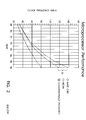
- Fig. 2 illustrates the performance advantages achieved over conventional packaging by use of multichip modules. As is evident from the graph, the performance gap 30 inherent with multichip modules is significantly smaller than that incurred with conventional packaging.
- the typical multichip module has several disadvantages that limit system performance, reduce yield and restrict the availability of multichip modules to a relatively small field of select users. Certain of these disadvantages stem from the use of polyimide and other organic materials as a dielectric. The raw material necessary to form the polyimide dielectric costs more than silicon-based materials and requires more processing steps to form the completed product. These characteristics of polyimide-dielectrics increase the cost of multichip modules and decrease the yield.
- polyimide has poor thermal conductivity and a thermal expansion coefficient that differs from silicon based ICs. Polyimide structures therefore often require additional thermal metal pillars under the die to ensure adequate heat conduction and balanced thermal stresses. The area consumed by the pillars is unavailable as interconnect. Also, the polyimide dielectric is under tension after processing, and that tension, when coupled with metal film tension, results in a highly bowed, internally stressed structure. The bowed structure can cause module reliability problems. Finally, the polyimide has a tendency to absorb moisture. This characteristic can reduce part life and requires that special measures be taken to prevent corrosion.
- the doped silicon has a much higher current spreading resistance than a metal film. Furthermore, the requirement that the substrate be highly doped adds significantly to the module materials costs.
- Preferred embodiments of the present invention may provide a mutlichip module which overcomes the aforementioned limitations of currently available multichip modules as well as providing additional advantages.
- power and ground planes comprising layers of anodizable metals are formed over the entire top surface of a nonconductive wafer which may be formed of silicon.
- a layer of dielectric material is disposed between the power and ground planes and is formed by the anodization of the metal. The resulting integral decoupling capacitor reduces the amount of patterning necessary to form the module and thus reduces costs.
- contact is made directly to the power and ground planes through vias.
- the direct connection frees the underlying support base from any requirement of electrical conductivity and permits the support base to be formed of undoped silicon or polysilicon or other materials further reducing module costs and also improving electrical performance.
- a thick layer of silicon dioxide is used in lieu of the polyimide dielectric.
- the silicon material does not absorb moisture and requires fewer processing steps than the polyimide material.
- the silicon dioxide can be deposited under controlled stress to control module camber and balance the processing stresses of the module. The silicon dioxide is deposited to thicknesses of 20pm without cracking.
- a diamond or boron nitride loaded epoxy material is used to mechanically attach the integrated circuit to a multichip module, also called a silicon circuit board (SiCB).
- the epoxy material increases the thermal conductance of the epoxy for improved heat dissipation without substantially increasing the capacitances of any signal line running underneath the epoxy.
- the epoxy material is loaded with high atomic weight particles to facilitate X-ray inspection of the adhesive for voids.
- reverse wedge wire bonding of the integrated circuits to the SiCB is used.
- the reverse wedge wire bonding improves the wire feed-to-adjacent chip clearances and allows integrated circuits to be spaced closer to each other on the chip.
- the module/integrated circuit assembly is mounted directly on the printed circuit board.
- the SiCB leads are wired directly to the circuit board.
- a multichip module having interconnect layers is provided with a termination resistor for the interconnect layers.
- a process for fabricating these termination resistors is provided.
- the metal interconnect layers are electrically connected by wirestrapping.
- the wirestrapping reduces the resistance of the interconnect lines without significantly increasing capacitance.
- the metal interconnect layers may also be formed and patterned so as to provide the module with multiple sets of bond pads.
- the multiple padout structure accomodates more than one manufacturer's IC and permits circuit designers to second source in a given bond pad location on the multichip module system IC components.
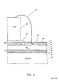
- Fig. 3 shows a cross-sectional view of a multichip module fabricated according to an embodiment of the present invention.
- the module contains a support base 40 over which are located power and ground planes 42 and 44. Because contact to power and ground planes 42 and 44 can be made directly to the metal comprising these planes, the support base 40 need not be conductive. For this reason, there is no need to dope support base 40, and support base 40 can be formed of silicon or polycrystalline silicon or other materials. Support bases of any shape may also be used.
- the absence of electrical requirements on the material comprising support base 40 means support base 40 can be manufactured from raw silicon ingots, including the end portions that would normally be treated as scrap material. Raw material costs are thereby reduced and the additional processing step of doping the silicon, eliminated.
- silicon has various performance advantages. Silicon has high thermal conductivity and also provides a good thermal expansion match to the rest of the multichip package and the attached ICs. Other materials, however, also can be used to form support base 40. These materials include AIN, A1 2 0 3 and copper-tungsten alloy. In addition, a composite sandwich structure of silicon and BeO may be used to match the thermal expansion properties of GaAs, as opposed to silicon-based chips.
- a conducting plane which in the embodiment of Fig. 3 comprises a power plane 42 and ground plane 44; which in turn are separated from support base 40 by an oxide layer 46.
- Optional oxide layer 46 provides electrical isolation and also forms a metallurgical barrier that prevents interaction of the aluminum with the silicon.
- Power and ground planes 42 and 44 are composed of layers of aluminum.
- Other electrically conductive materials may also be used, provided the upper surface of conductive layer 44 is formed of anodizable material.
- a copper conductive layer with tantalum adhesive layer may be used to comprise layer 44.
- Separating power plane 42 from ground plane 44 is a dielectric layer 48 of A1 2 0 3 formed by anodization of the aluminum layer 44.
- the anodization process provides a pinhole-free capacitor dielectric and improved electrical performance.
- a layer of silicon dioxide or silicon nitride may optionally be placed over the A1 2 0 3 layer to further improve the pinhole-free properties of the A1 2 0 3 layer.
- Ground plane 44, power plane 42 and dielectric layer 48 form an integral decoupling capacitor 49.
- Capacitor 49 aids in reducing series inductance and ground bounce. Both power and ground planes and capacitor 49 are formed over the entire surface of the module and before any patterning of circuit interconnections takes place. This structural feature allows the capacitor size to increase as module size increases and eliminates the need for patterning during the formation of the capacitor. The elimination of the masking steps which make contact vias early in the process flow permits nearly completed modules to be placed in "inventory", thereby minimizing costs and shortening delivery time as will be explained below. It also substantially increases yields by greatly reducing the probability of particle contamination during fabrication of capacitor 49.
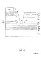
- FIG. 4 shows a cross-sectional view of a module in which a ground via 62 to ground plane 44 has been formed.
- a moat 63 electrically isolates power plane 42 from via 62.
- Direct contact to the power and ground planes relieves support base 40 from any requirement to be conductive and results in the advantages previously described. Direct contact to the metal also reduces spreading resistance further improving multichip performance.
- the module can be formed with fewer planes than that shown in Fig. 3 and the power and ground planes need not be arranged in the sequence shown. Multiple power and ground planes allow the module to provide multiple voltages to the ICs packaged on the module.
- the multichip module of the present invention is therefore suitable for use with a variety of semiconductor technologies; for example, CMOS, nMOS, GaAS, and bipolar technologies. Additional power and ground planes 64 and 65 are shown in Fig. 4. Contacts to these layers are elsewhere on the module and are not shown in the Fig.
- dielectric layer 70 Located on top of the power and ground planes is a dielectric layer 70 that insulates the power and ground planes 42 and 44 from metal signal carrying layers 76 and 77.
- dielectric layer 70 is formed of a silicon dioxide layer up to 2 0 ⁇ m thick. The thickness of the silicon dioxide layer provides low interconnect capacitance.
- silicon dioxide would not have been chosen as the material with which to form dielectric 70.
- Conventional processes deposit silicon dioxide under tension or extreme compression and thick layers of silicon dioxide deposited using these methods are thus prone to crack or induce delamination of the multilayer structures in Fig. 4.
- a layer of silicon dioxide having the thickness desired (aspm) to form a multichip module dielectric was therefore not feasible nor practical prior to the present invention.
- silicon dioxide is deposited under compression to provide benefits analogous to those achieved in tempered glass or prestressed concrete. Plasma-enhanced chemical vapor deposition of the silicon dioxide can be tightly controlled to match the other process stresses and virtually eliminate module camber.
- silicon dioxide does not absorb moisture as does the polyimide structure. Corrosion problems are thereby eliminated and the expense of encapsulating the module metal signal layers in barrier metals, avoided. Elimination of corrosion problem also permits non- hermetic packaging of the completed module/IC structure. Silicon dioxide also possesses better thermal characteristics than does polyimide. The improved thermal conductivity of silicon dioxide provides better heat dissipation thereby eliminating any requirement for thermal vias or pillars. The resulting module can withstand higher post-processing temperatures than modules incorporating the polyimide material.
- Metal signal, or interconnection, layers 76 and 77 reside on top of silicon dioxide layer 70 and carry signals among the ICs mounted on the module. In the structure of Fig. 3, the general orientation of connections in layer 77 is perpendicular to those in layer 76. A second dielectric layer of Silicon dioxide 78 separates metal signal layer 76 from metal signal layer 77.
- the metal interconnect layers can be formed of sputtered aluminum, sputtered copper or electroplated copper, gold and in some embodiments otherconduc- tive materials. Signal layers, in addition to those shown, can be formed to permit more than two signal connections.
- Metal signal layers 76 and 77 may also incorporate metal strapping techniques.
- the thin film metallization used to form metal signal layers 76 and 77 cover a significant distance on the module surface.
- the resistance of the layers due to length can therefore limit module performance. While the resistance of these layers can be reduced by increasing the thickness of the layers, the cost of fabricating each signal layer increases with the layer thickness.
- the metal strapping technique is especially useful for those signal paths where line resistance is of concern.
- Fig. 5 is a cross section of a 7metal signal layer formed using the metal strapping technique.
- Metal signal layers 76 and 77 are positioned one on top of the other. Layer 76 is shown slightly narrower than 77 as is standard practice to allow for manufacturing tolerances and avoid coincident edges.
- Layer 76 may also be formed slightly narrower than layer 77 to reduce fringe capacitance between the layers according to another embodiment of the invention. Layers 76 and 77 carry the same signal. The two layers are periodically tied together, for example, with vias 79a and 79b or with a trench (not shown). The metal strap technique reduces the resistance of signal lines without incurring a significant increase in capacitance.
- the electrical performance of the module may be further enhanced by removing areas of exposed dielectric 70 from everywhere except underneath the metal signal layers 76 and 77, to form the pedestal structure of Fig. 6.
- metal signal layers 76 and 77 reside on isolated pedestals of silicon dioxide 70 and 78. There is no requirement that 76 and 77 run parallel to each other although that is implied by Fig. 6. Reduced fringe and interconnect capacitance result, which further reduce signal propagation delays and system power consumption.
- the metal strapping technique of Fig. 5 also may be used in conjunction with the pedestal structure of Fig. 6.
- Termination resistors also may be formed at the ends of metal signal layers 76 by the addition of extra processing steps.
- the termination resistors are made with the same design rules (line widths and spacings) used to form the interconnect layers and therefore consume no additional module area. Since the geometry and electrical properties of the metal film(s) used to form layers 76 and 77 are known, the area of the termination resistor can be easily determined and the metal film patterned to provide the desired resistance.
- passivation layer 8b On top of metal signal layers 76 and 77 is indicated a passivation layer 8b. See Fig. 3.
- Passivation layer 80 preferably formed of a silicon dioxide layer 84 with a silicon nitride cap 86, select to isolate the module layers from contaminant and protect the module from abrasions.
- the IC 90 is mechanically mounted on the module by a layer of thermally conductive adhesive 94 located above passivation layer 80.
- the adhesive is also preferably electrically insulating without having an enormously high dielectric current.
- a boron nitride or diamond loaded epoxy comprises the adhesive material. These materials increase the thermal conductivity of the epoxy for improved heat dissipation without substantially increasing the capacitance of signal lines running underneath the epoxy.
- Adhesive 94 may also be loaded with high atomic weight particles to facilitate x-ray inspection of the adhesive for voids in the adhesive die attachment. The high atomic weight particles should have an atomic number high enough to be conveniently exposed by X-ray, yet low enough so as not to be opaque. Germanium and/or oxides of transition elements and/or oxides of rare earth metals are examples of suitable material. Electrically conductive adhesive (e.g., silver-filled) may also be used if back-side contact for the IC is required.
- back-side contact may be had using the nonelectrically conductive, yet thermally conductive epoxy materialss described above by depositing a layer of this epoxy such that a hole remains in which the SiCB bond pad is exposed A layer of electrically conductive epoxy may then be deposited over this layer to allow back-side contact.
- This dual layer attachment structure provides improved thermal conductance without substantially increasing the capacitance of metal signal layers running underneath the IC over the single layer silverfilled epoxy attachment structure. Additionally, the silverfilled epoxy layer can be omitted and a wire run from the back side of the IC through the hole in the nonelectrically conducting adhesive to the SiCB bond pad.
- IC 90 Electrical connection of IC 90 to the module can be accomplished using reverse wedge wire bonding to attach the IC leads 98 to bonding or die pads (not shown).
- IC 90 may be electrically connected to the multichip module using conventional wire bonding or flip chip technology.
- the pads connect to the underlying metal layers through vias. Because connection to the decoupling capacitor and termination resistors is provided elsewhere on the module through these vias, surface mounting of capacitors and resistors, and direct mechanical connection of these devices to the multichip module are not required. For this reason, IC 90 can be placed extremely close to the module bonding pad and to neighboring ICs.
- Fig. 7 compares the space consumed by conventional wire bonding 100 with that used by reverse wedge wire bonding 102 used to connect IC 90 to the module bond pads according to an embodiment of the present invention.
- reverse wire wedge bonding the bond is made first to the module bond pads and then to the chip.
- reverse wedge wire bond techniques improve wiring densities over conventional wire bonding techniques because the wire feed of reverse wedge wiring tool 101 requires less clearance than the wire feed of conventional tool 103. The improved clearances also permit the interleaving of the wire bonds.
- This reverse wedge wire bond technique in combination with the elimination of surface mounted decoupling capacitors and termination resistors, therefore, greatly improves chip densities, allowing approximately seventy-five percent of the module surface to be covered with ICs 90.
- the improved chip densities that stem from the structure of the termination resistors, decoupling capacitor and wire bonding/substrate-on-board mounting techniques permits the multichip module of the present invention to economically support more than one bond pad configuration and, therefore, more than one circuit or system.
- bond pads and leads are of such a dimension that a multiple padout scheme would impact board performance.
- a multiple padout structure for a multichip module according to the present invention is shown in Fig. 8 where pads 120 support one circuit configuration. Pads 124 support a second circuit configuration.
- the multiple padout structure means that a single multichip module of the present invention can economically support more than one chip geometry and that each multichip module need not be application-specific.
- the multiple padout structure allows different manufacturer's memory chips to be used on the same SiCB.
- Fig. 9 shows a module to which a number of ICs 90 have been attached.
- the module with attached ICs can be enclosed in a hermetically sealed package 128 and connected to the remainder of the system by package leads 130 to a printed circuit board.
- a heat sink 132 may be mounted on the back of package 128.
- a substrate-on-board technique may be used to mount the module to the circuit board.
- the module identified by reference numeral 134 is mounted face down and the module bond pads are wired directly to the printed circuit board 140.
- Other methods of electrical attachment besides wire bonding may be used.
- tape may be used.
- Wire bonds 138 connect the IC 90 to the module.
- a heat sink 137 cools thesystem.
- the substrate on board permits elimination on the hermetic package.
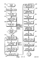
- FIG. 11-1 through 11-2 A process for fabricating the multichip module of the present invention is described by reference to the flow chart contained in Figs. 11-1 through 11-2.
- fabrication of the structures of Figs. 3 and 6 will be used as an illustrative example. All references to the structure of the completed multichip module may therefore be found in Figs. 3 and 6 unless otherwise noted. All references to process steps may be found in Figs. 11-1 through 11-2.
- the process begins at step 200 with an unprocessed standard-size wafer.
- a standard-size wafer has a typical diameter of 125mm and thickness of 0.5mm. Nonstandard size wafers also may be used and various shapes other than a wafer may be used.
- the unprocessed wafer may be formed from various materials, including: Al 2 O 3 , AIN, copper-tungsten alloy, a composite sandwich structure of BeO, quartz, glass or other well known materials.
- the wafer is composed either of silicon or of polycrystalline silicon and forms support base 40 of the multichip module.
- oxide layer 46 is thermally grown in step 202 on the top surface of wafer 40 to a thickness of approximately 0.8 ⁇ m.
- a metal film which can be an aluminum film, or other conductor having a top surface of anodizable metal, e.g., a Ta/Cu/Ta sandwich; is deposited over oxide layer46 in step 204.
- This metal film, or metal layer M o eventually forms ground plane 44 seen in Fig. 3.
- the aluminum film is deposited on top of oxide layer 46 using vacuum deposition techniques well known to those of skill in the art.
- a preferred embodiment of the invention uses sputtering vacuum deposition. The deposition processes deposit a film of aluminum approximately 1.25 to 2.25 ⁇ m thick over the entire surface of the structure.
- a layer of Al 2 O 3 approximately 0.2 ⁇ m thick is formed by anodizing metal layer M o in step 206.
- the anodization process consumes a portion of layer M o , leaving an M o layer of approximately 1-2 ⁇ m.
- the resulting A1 2 0 3 layer serves as dielectric 48 and is formed over the entire surface area of the module structure. If layer M o comprises a material other than aluminum, the anodization process forms the oxide of the material used.
- a second vacuum deposition of a metal film over the entire surface of the structure occurs in step 208.
- This metal layer, M l forms power plane 42 and also is composed of aluminum in a preferred embodiment. If layer M 1 comprises the final power/ground layer, the metal film is deposited to a thickness of 1-2 ⁇ m.
- Fig. 3 depicts only a single power and a single ground plane, multiple power and ground planes may be formed to permit connection of IC 90 to multiple voltages. If additional metallization is desired, steps 206 and 208 of the process are repeated. Metal layer M 1 should therefore be deposited to a thickness of 1.25 to 2.25 ⁇ m to allow for the consumption of material during the anodization process.
- step 208 of the process the structure shown in Fig. 12 results. Openings must thus be formed through layers 42 and 48 to permit contact to layer M o , which forms ground plane 44.
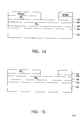
- the openings are patterned in step 210 using photolithography techniques well known in the art to form the structure shown in Fig. 13. A wet chemical etch, etches those areas of metal M 1 not covered by resist to expose Al 2 O 3 layer 48 and form the structure of Fig. 14. The resist may then be removed using conventional methods. Using the remaining metal M 1 as a mask, the exposed areas of Al 2 O 3 are etched with a chemical etch comprising a mixture of Cr0 3 and H 3 PO 4 in water at approximately 65-85°C.
- step 212 the structure of Fig. 15 having via 62 to plane 44 results.
- M 1 must then be electrically isolated from via 62 used to contact layer M o by completing step 214.
- Metal M 1 is again masked using conventional photolithography and etched with a wet chemical etch to remove metal M 1 in areas 217 and 218 adjacent to the via. Any other desired cuts in M 1 , e.g., to create isolated power planes, can also be made at this time. See Fig. 16. An annular top surface of Al 2 O 3 is thus left exposed. Vias to the desired metal layers are formed by repeating steps 210 and 212 (and 214, if applicable).
- steps 210, 212, 214 can be used when an Al 2 O 3 etch is available which does not attack adversely photoresist (for example, a BC1 3 plasma or certain wet etches).
- M 1 can be processed conventionally like step 210 except that all desired cuts in M 1 are done atthis step, rather than as part of step 214.
- the photoresist is then stripped.
- a new photoresist pattern is then created with vias concentric with but inside the openings in M 1 (where ground contacts are desired).
- the Al 2O 3 is then etched and the photoresist is stripped. This process flow is simpler because step 214 is eliminated and yields a more capacitive ground contact, but requires an etchant other than the hot H 3 PO 4 /CrO 3 /H 2 O mixture described above (which can attack photoresist).
- step 210 layer M 1 is patterned and etched in step 210 at those locations where a contact to the underlying metal layer M o is ultimately desired.
- Step 212 which etches the dielectric layer and step 214 are not conducted at this time.
- the process flow proceeds directly to step 222 as indicated by arrow 223 exiting box 210.
- a thick layer of Si0 2 is deposited over the structure in step 222.
- the layer of Si0 2 forms dielectric 70 and is deposited to a thickness of 7-15 ⁇ m using plasma-enhanced chemical vapordep- osition. Thicknesses of up to 20 ⁇ m may be deposited, if necessary, to provide the desired low capacitance of the signal layers 76 and 77 relative to the power and ground layers.
- the Si0 2 is deposited so as to yield moderate in-plane biaxial compressive stress. Generally, the residual compressive oxide stress on the substrate should be kept to under 1 X 10 9 dynes/cm 2 .
- One method for depositing the silicon under compression using plasma-enhanced chemical vapor deposition to achieve these stress limits is described in the U.S. Patent Application to Schoenholtz for Improved Plasma Enhanced Chemical Vapor Deposition Process referenced above.
- step 224 silicon dioxide dielectric layer 70 is patterned using photolithography techniques and etched to expose the vias to metal layer M o , and to create via contacts to metal layer M 1 where needed.
- the patterning and etching step of 224 comprises opening vias to metal layer M, as desired and also opening vias to expose those portions of the dielectric layer not covered by metal M 1 .
- the exposed portion of the dielectric layer can then be etched away by dipping the module into a H 3 PO 4 /Cro 3 /H 2 O etchant to open a via for the M o contact.
- the process flow incorporating arrow 223 thus reduces a mask step over the other possible processes described herein thereby further reducing module cost.
- step 230 the aluminum is sputter deposited and patterned to form metal signal layer 76, or M 2 , which typically has a thickness of 2-3 ⁇ m.
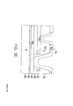
- Metal signal layer 76 may therefore be constructed as a three-layer metal sandwich as shown in Fig. 18.
- the sandwich structure comprises a tantalum nitride layer 246, a copper layer 248 and a tantalum upper layer 250.
- tantalum nitride may be used to construct upper layer 250.
- Tantalum nitride layer 246 ultimately forms a termination resistor at the completion of the fabrication process but also serves as an adhesive layer.
- Copper layer 248 carries the signal and tantalum layer 250 serves as an optional adhesion layer between the upper surface of copper layer 248 and overlying Si0 2 .
- the sandwich signal layer structure of Fig. 18 is obtained from Fig. 17 by depositing a tantalum nitride layer 246 approximately 0.2wm thick over dielectric 70. See step 260. Over this layer of tantalum nitride, in step 230, is sputter deposited copper layer 248 to a thickness of 3-4 ⁇ m. Layer 250 of tantalum may then deposited to a thickness of ⁇ 0.05 ⁇ m over copper layer 248 if desired to complete formation of the metal signal layer in step 230. The composite metal structure thus totals 3-4wm.
- step 262 the signal layer deposited in step 230 is patterned and etched to permit contact to underlying layers. If the metal signal layer is constructed with the termination resistor structure, layer 250 of tantalum must be etched away at those locations where a contact to signal carrying copper layer 248 and to termination resistor layer 246 is desired. A dry etch removes layer 250 in step 268. Copper layer 248 is also etched in step 268 to expose resistor layer 246.
- Fig. 19 shows an isometric view of a composite metal signal layer including termination resistor contact 272 upon completion of step 268.
- Fig. 20 depicts the partially completed multichip module structure after metallization of signal layer 76 with either aluminum or copper as described above.
- an insulating layer 78 of Si0 2 is deposited over metal layer M 2 in step 280 to form layer 78.
- Layer 78 is deposited using plasma-enhanced chemical vapor deposition.
- step 282 layer 78 of Si0 2 is then patterned and etched to open vias to underlying metal layer M 2 where desired.
- the silicon dioxide remaining over layer M 2 has a typical thickness of 3wm.
- a second metallization occurs to form layer M 3 , which may be used to form metal signal layer 77 of Fig. 3.
- the layer may be formed in a single deposition step 284. If the metal film is composed of another metal such as copper, then a composite metal sandwich structure must be built to form signal layer 77. The process for fabricating this structure occurs in steps 285-289 and is somewhat analogous to the process of steps 260-264 except that termination resistors are not formed.
- Metal signal layer 77 has a thickness approximating 3-4 ⁇ m when completed. Additional metal signal layers other than the two layers depicted in Fig. 3 are formed by repeating steps 260 to 294.
- layer M 3 forms an independent signallayerfrom M 2 , then layer M 3 will often be oriented perpendicular to layer M 2 as shown in Fig. 21 B. If the wire strap method of Fig. 5 is used, then layer M 3 runs over layer M 2 as shown in Fig. 21A. Note that layer M 3 has slightly different width than layer M 2 to avoid coincident edges. Whether or not a metal strap structure is employed, metal M 3 is then patterned and etched in step 294 to form the desired interconnect pattern. When M 3 is formed of a composite metal structure, sequential etches are performed in step 294 to remove the metal layers.
- step 298 must be performed.
- the metal layers 76-77 are used as a mask for an anisotropic etch of the underlying silicon dioxide dielectric layers 78 and 70.
- Fig. 21A depicts an isometric view of the multichip module with wire strapping upon completion of these steps and Fig. 21 B depicts the structure with two distinct signal layers oriented at a ninety degree angle to each other.
- a passivation layer 80 is deposited in step 320.
- the passivation layer comprises silicon dioxide layer 84 over which a silicon nitride cap 86 is placed.
- the silicon dioxide and silicon nitride are deposited using plasma-enhanced chemical vapor deposition.
- Passivation layer 80 is approximately 2-6pm thick, and serves to protect the module from abrasions and contaminants.
- the passivation layer 80 is then patterned and etched in step 322 to expose pads for wire bonding of IC 90 to the module. Formation and etch of the passivation layer completes wafer fabrication.
- step 324 Assembly of the wafer and ICs into multichip modules begins by separating the completed wafer into individual modules, or silicon circuit boards (SiCB), using a wafer saw. See step 324. If the module is to be conventionally mounted, step 326 of the fabri- cation/assembly process places the module in a hermetic package that contains leads for later mounting of the module/chip assembly to a circuit board. In step 328, ICs 90 are bonded to the SiCB. The ICs 90 are electrically connected to the SiCB using reverse wire wedge bonding as described in Fig. 8. See step 330. The reverse wire wedge bond consumes less surface area on the module and permits greater chip densities. Wire bonds are also made between the package and the SiCB. See step 336. The completed conventional package is as depicted in Fig. 9.
- the SiCB is first mounted to a rigid backing such as copper tungsten in step 338 to form a support structure.
- the backing should preferably have a thermal expansion closely matched to the SiCB and a good thermal conductor. Examples of possible backing materials include molybdenum and a copper/Invar sandwich in addition to the copper tungsten material mentioned above.
- Chips are then attached in step 340. The chips are wire bonded to the SiCB and then the chips, or interior surface portions of the SiCB encapsulated, e.g. with epoxy.
- the entire assembly is then mounted to the printed circuit board, wire bonded and encapsulated.
- the electrical connection of the SiCB to the circuit board may be accomplished using other procedures known to those of skill in the art, such as tape for example. See steps 334-348 of Fig. 11.
Landscapes
- Semiconductor Integrated Circuits (AREA)
- Wire Bonding (AREA)
- Die Bonding (AREA)
- Lead Frames For Integrated Circuits (AREA)
- Internal Circuitry In Semiconductor Integrated Circuit Devices (AREA)
Applications Claiming Priority (8)
| Application Number | Priority Date | Filing Date | Title |
|---|---|---|---|
| US62985190A | 1990-12-17 | 1990-12-17 | |
| US62974690A | 1990-12-17 | 1990-12-17 | |
| US07/630,469 US5134539A (en) | 1990-12-17 | 1990-12-17 | Multichip module having integral decoupling capacitor |
| US630469 | 1990-12-17 | ||
| US629731 | 1990-12-17 | ||
| US629851 | 1990-12-17 | ||
| US07/629,731 US5214844A (en) | 1990-12-17 | 1990-12-17 | Method of assembling integrated circuits to a silicon board |
| US629746 | 2000-07-31 |
Publications (2)
| Publication Number | Publication Date |
|---|---|
| EP0492933A2 true EP0492933A2 (fr) | 1992-07-01 |
| EP0492933A3 EP0492933A3 (en) | 1993-03-03 |
Family
ID=27505189
Family Applications (1)
| Application Number | Title | Priority Date | Filing Date |
|---|---|---|---|
| EP19910311696 Withdrawn EP0492933A3 (en) | 1990-12-17 | 1991-12-17 | Multichip module |
Country Status (3)
| Country | Link |
|---|---|
| EP (1) | EP0492933A3 (fr) |
| JP (2) | JP3249162B2 (fr) |
| CA (1) | CA2057744C (fr) |
Cited By (3)
| Publication number | Priority date | Publication date | Assignee | Title |
|---|---|---|---|---|
| EP1223617A3 (fr) * | 2000-12-22 | 2004-02-18 | Matsushita Electric Industrial Co., Ltd. | Module multi-puces avec une pluralité de puces semi-conductrices montées sur un substrat semiconducteur |
| WO2007145596A1 (fr) * | 2006-06-14 | 2007-12-21 | Ternary Technologies Pte Ltd | dispositif moteur léger et son procédé de fabrication |
| CN118522699A (zh) * | 2024-05-13 | 2024-08-20 | 江苏索力德普半导体科技有限公司 | 一种高功率密度高散热性的dbc基板及功率模块 |
Families Citing this family (1)
| Publication number | Priority date | Publication date | Assignee | Title |
|---|---|---|---|---|
| JP3873717B2 (ja) | 2001-11-09 | 2007-01-24 | ソニー株式会社 | 正極材料およびそれを用いた電池 |
Family Cites Families (1)
| Publication number | Priority date | Publication date | Assignee | Title |
|---|---|---|---|---|
| DD281076A1 (de) * | 1989-03-31 | 1990-07-25 | Robotron Veb K | Verfahren zur herstellung eines mehrebenensubstrates |
-
1991
- 1991-12-16 CA CA002057744A patent/CA2057744C/fr not_active Expired - Lifetime
- 1991-12-17 JP JP36104591A patent/JP3249162B2/ja not_active Expired - Fee Related
- 1991-12-17 EP EP19910311696 patent/EP0492933A3/en not_active Withdrawn
-
2001
- 2001-08-28 JP JP2001258274A patent/JP3374138B2/ja not_active Expired - Fee Related
Cited By (3)
| Publication number | Priority date | Publication date | Assignee | Title |
|---|---|---|---|---|
| EP1223617A3 (fr) * | 2000-12-22 | 2004-02-18 | Matsushita Electric Industrial Co., Ltd. | Module multi-puces avec une pluralité de puces semi-conductrices montées sur un substrat semiconducteur |
| WO2007145596A1 (fr) * | 2006-06-14 | 2007-12-21 | Ternary Technologies Pte Ltd | dispositif moteur léger et son procédé de fabrication |
| CN118522699A (zh) * | 2024-05-13 | 2024-08-20 | 江苏索力德普半导体科技有限公司 | 一种高功率密度高散热性的dbc基板及功率模块 |
Also Published As
| Publication number | Publication date |
|---|---|
| JP3374138B2 (ja) | 2003-02-04 |
| JPH06132467A (ja) | 1994-05-13 |
| JP3249162B2 (ja) | 2002-01-21 |
| CA2057744C (fr) | 2003-09-23 |
| CA2057744A1 (fr) | 1992-06-18 |
| EP0492933A3 (en) | 1993-03-03 |
| JP2002124621A (ja) | 2002-04-26 |
Similar Documents
| Publication | Publication Date | Title |
|---|---|---|
| US5134539A (en) | Multichip module having integral decoupling capacitor | |
| US5274270A (en) | Multichip module having SiO2 insulating layer | |
| US5648684A (en) | Endcap chip with conductive, monolithic L-connect for multichip stack | |
| US6673698B1 (en) | Thin film semiconductor package utilizing a glass substrate with composite polymer/metal interconnect layers | |
| CN1314117C (zh) | 集成电路封装结构及集成电路封装方法 | |
| US6746898B2 (en) | Integrated chip package structure using silicon substrate and method of manufacturing the same | |
| US5481133A (en) | Three-dimensional multichip package | |
| CA1232367A (fr) | Groupement de dispositifs microminiature | |
| US7511376B2 (en) | Circuitry component with metal layer over die and extending to place not over die | |
| US6984886B2 (en) | System-on-a-chip with multi-layered metallized through-hole interconnection | |
| US5521434A (en) | Semiconductor chip and electronic module with integrated surface interconnects/components | |
| US7781887B2 (en) | Semiconductor device including an interconnect | |
| JP2001507520A (ja) | 集積回路パッケージングのための構造体及び方法 | |
| EP1483789A2 (fr) | Dispositif a semi-conducteurs a plot de connexion de fils et procede a cet effet | |
| JP2011155310A (ja) | 半導体装置並びに配線基板及びその製造方法 | |
| US5376574A (en) | Capped modular microwave integrated circuit and method of making same | |
| US5214844A (en) | Method of assembling integrated circuits to a silicon board | |
| CN117747587A (zh) | 封装载板及其制作方法、半导体器件及半导体组件 | |
| CA2057744C (fr) | Module multipuce | |
| US7135779B2 (en) | Method for packaging integrated circuit chips | |
| US8008134B2 (en) | Large substrate structural vias | |
| US7390697B2 (en) | Enhanced adhesion strength between mold resin and polyimide | |
| JP2601640B2 (ja) | 電気的導体構造を作成する方法と大規模集積回路 | |
| Reichl | Silicon substrates for chip interconnection | |
| JPH04230067A (ja) | 精密に形成したチップを近接して配設することによりウェーハのスケールを集積化する方法 |
Legal Events
| Date | Code | Title | Description |
|---|---|---|---|
| PUAI | Public reference made under article 153(3) epc to a published international application that has entered the european phase |
Free format text: ORIGINAL CODE: 0009012 |
|
| AK | Designated contracting states |
Kind code of ref document: A2 Designated state(s): DE FR GB IT |
|
| RIN1 | Information on inventor provided before grant (corrected) |
Inventor name: THALAPENENI, GARUNADA N Inventor name: LANG, CHARLES R Inventor name: TUCKERMAN, DAVID B Inventor name: MHASKER, PANDHARINATH A Inventor name: BOBRA, YOGENDRA Inventor name: MCWILLIAMS, BRUCE M Inventor name: BENSON, DONALD Inventor name: SCHOENHOLTZ, JOSEPH JR |
|
| PUAL | Search report despatched |
Free format text: ORIGINAL CODE: 0009013 |
|
| AK | Designated contracting states |
Kind code of ref document: A3 Designated state(s): DE FR GB IT |
|
| 17P | Request for examination filed |
Effective date: 19930824 |
|
| 17Q | First examination report despatched |
Effective date: 19941214 |
|
| STAA | Information on the status of an ep patent application or granted ep patent |
Free format text: STATUS: THE APPLICATION IS DEEMED TO BE WITHDRAWN |
|
| 18D | Application deemed to be withdrawn |
Effective date: 19950425 |