EP0492987B1 - Kupferlegierungen und daraus hergestellte Leitergitter - Google Patents
Kupferlegierungen und daraus hergestellte Leitergitter Download PDFInfo
- Publication number
- EP0492987B1 EP0492987B1 EP91311805A EP91311805A EP0492987B1 EP 0492987 B1 EP0492987 B1 EP 0492987B1 EP 91311805 A EP91311805 A EP 91311805A EP 91311805 A EP91311805 A EP 91311805A EP 0492987 B1 EP0492987 B1 EP 0492987B1
- Authority
- EP
- European Patent Office
- Prior art keywords
- lead frame
- less
- weight
- alloy
- partial
- Prior art date
- Legal status (The legal status is an assumption and is not a legal conclusion. Google has not performed a legal analysis and makes no representation as to the accuracy of the status listed.)
- Expired - Lifetime
Links
Images




Classifications
-
- H—ELECTRICITY
- H10—SEMICONDUCTOR DEVICES; ELECTRIC SOLID-STATE DEVICES NOT OTHERWISE PROVIDED FOR
- H10W—GENERIC PACKAGES, INTERCONNECTIONS, CONNECTORS OR OTHER CONSTRUCTIONAL DETAILS OF DEVICES COVERED BY CLASS H10
- H10W70/00—Package substrates; Interposers; Redistribution layers [RDL]
- H10W70/40—Leadframes
- H10W70/456—Materials
-
- C—CHEMISTRY; METALLURGY
- C22—METALLURGY; FERROUS OR NON-FERROUS ALLOYS; TREATMENT OF ALLOYS OR NON-FERROUS METALS
- C22C—ALLOYS
- C22C9/00—Alloys based on copper
Definitions
- the present invention relates to a lead frame and the material of which the frame is made, being a Cu alloy.
- a lead frame made of a Fe-Ni alloy such as 42wt%Ni-Fe or 29wt%Ni-17wt%Co-Fe has a coefficient of thermal expansion very similar to that of the semiconductor element.
- a lead frame made of a Fe alloy is expensive because expensive components such as nickel and cobalt are used.
- a lead frame made of a Fe alloy doesn't satisfy the requirements of high radiation, that is, thermal conductivity, which is required as semiconductors become highly integrated.
- lead frames made of a Cu alloy are chiefly being used because of the property of high radiation and lower costs.
- Cu-Cr-Zr alloy is especially being used because of its high hardness and high conductivity (EP-A-0 114 338).
- the lead frame made of a Cu-Cr-Zr alloy as described above often has a peeling part on the surface of the lead frame, and a plating scab caused by heat treatment when the surface is coated.
- a Cu-Cr-Zr alloy as described above is required to have high conductivity with a good producibility, for example not less than 75IACS%, for the high efficiency of a lead frame.
- the present inventors have made extensive studies, and found that the problems such as peeling parts on the surface of the lead frame and a scab on the lead frame caused by heat treatment when being plated and the like are due to the number of partial discoloured regions, and further more, the partial discoloured regions are due to the unbalanced precipitation of Zr.
- the present invention has been made based on this finding and has for its object to provide a lead frame and a material of the same which has a high conductivity and which makes it possible to produce a highly reliable IC package or a LSI package and the like with a high yield of production.
- a material of the present invention suitable for making a lead frame comprises a copper alloy which contains 0.1 to 1% by weight of Cr, 0.01 to 0.5% by weight of Zr less than 0.005% S and having a partial discoloured region caused by unbalanced precipitation of the Zr distributed thereon at a rate of 2 grains/100cm2 or less, the balance being Cu apart from impurities.
- the invention also embraces a lead frame constructed of the aforesaid material.
- the number of partial discoloured regions caused by unbalanced precipitation of Zr has been found to be an important feature in the present invention.
- the number of partial discoloured regions caused by unbalanced precipitation of Zr is 2 grains/100cm2 or less, the problems such as plating scabs on the lead frame caused by heat treatment are improved, which makes it possible to produce a highly reliable IC package or LSI package and the like with a high yield of production.
- the number of these partial discoloured regions is preferably 1 grain/100cm2 or less.
- the number of partial discoloured regions is more preferably zero.
- the phrase "partial discoloured regions caused by unbalanced precipitation of Zr" is used in this description and the claims to mean a region which has a different colour from other regions, which can be observed by microphotograph.
- the region is usually belt-shaped.
- the partial discoloured region is normally an independent region.
- the partial discoloured region caused by unbalanced precipitation of Zr has been found to at least partly depend on the sulphur content. Consequently it is preferred to restrict the sulphur content, which may be an impurity in the alloy, to less than 0.005% by weight. If the sulphur content is less than 0.005% by weight, the number of partial discoloured regions caused by unbalanced precipitation of Zr can be 2 grains/100cm2 or less. The said sulphur content is more preferably less than 0.004% by weight, but even more preferably less than 0.003% by weight. In addition, the number of partial discoloured regions caused by unbalanced precipitation of Zr has also been found to be at least partly influenced by the method of incorporating Zr in the alloy. Adding Zr in the form of a matrix alloy of Cu-Zr is preferable to reduce formation of said partial discoloured regions.
- the preferred composition of the Cu alloy of the present invention can be specified by the following optional limitations.
- the Cr content is 0.1% by weight or more, the mechanical strength and heat resistance of the alloy are increased. This effect is maintained without impairing the bending strength and electrical conductivity of the alloy until the Cr content reaches 1% by weight.
- the value of the Cr content is preferably in the range from 0.2-0.6% by weight.
- the value of the Cr content is more preferably in the range from 0.2-0.5% by weight.
- the Zr content is 0.01% by weight or more, the mechanical strength and heat resistance of the alloy are increased. This effect is maintained without impairing the bending strength and electrical conductivity of the alloy until the Zr content reaches 0.5% by weight.
- the value of the Zr content is preferably in the range from 0.05-0.3%by weight.
- the value of the Zr content is more preferably in the range from 0.05-0.25% by weight.
- the lead frame material of the present invention preferably has high electrical conductivity, which is not less than 75IACS%. If the conductivity is 75IACS% or more, a higly efficient lead frame can be made of the alloy for use with a highly integrated semiconductor element.
- the electrical conductivity of the lead frame is more preferably 80IACS% or more.
- the electrical conductivity of the lead frame is even more preferably 85IACS% or more.
- the impurities in the alloy are preferably less than 0.05% by weight of Fe, less than 0.1% by weight of Ni, less than 0.05% by weight of P, less than 0.1% by weight of Sn and less than 0.1% by weight of Zn.
- the effects mentioned above can be maintained without impairing the electrical conductivity of the alloy, so long as any such impurity present does not exceed these preferred limits.
- the content of each of these elements is more preferably less than 0.05% by weight of Ni, less than 0.03% by weight of P, less than 0.05% by weight of Sn and less than 0.05% by weight of Zn.
- the lead frame and the alloy material from which it can be made are improved if the following conditions are met.
- the peeling part on the surface of the lead frame is preferably 5 grains/coil or less. If an IC package or a LSI package is produced using a lead frame with a peeling part on the surface of the lead frame of more than 5 grains/coil, a highly reliable package is not obtained, because of impairment of the yield production caused by the peeling parts.
- the value of the peeling part is preferably not more than 3 grains/coil, and the value of the peeling part is more preferably zero.
- peeling part as used in this description and the claims means the condition when a portion of the surface peels linearly from the surface of the lead frame.
- plating scab means a convex part which seems to be swollen up from the plating face.
- Plating scabs can be detected by confirming the flattness of the plated face after performing plating, and thereafter by observing the surface by stereomicroscope ( ⁇ 20) after performing hot working at 350°C for 5 minutes.
- the Vickers hardness of the lead frame is preferably 150Hv or more.
- the Vickers hardness is not less than 150Hv, a highly reliable package having sufficient hardness can be produced.
- the value of the Vickers hardness is preferably not less than 160Hv.
- the value of the Vickers hardness is more preferably not less than 170Hv.
- Cu alloy having the compositions as shown in Table-1 were prepared by casting after smelting under vacuum in a carbon crucible and an ingot was produced. Hot forging after heating to about 900°C was then performed in order to form each ingot to a billet having a thickness of about 150mm and a width of about 450mm. Next, hot rolling after heating to about 950°C was then performed in order to form each billet to a hot coil having a thickness of about 13mm and a width of about 450mm. After performing hot working at 750°C to 800°C, in conclusion, a solution treatment was performed by rapid cooling.
- the number of partial discoloured regions were investigated in the range of 10cm ⁇ 10cm, and the average value of them was measured at 10 different ranges.
- Table-2 shows the results of the above mentioned evaluation.
- the Vickers hardness of the samples was measured, and the electrical conductivities were calculated by measuring relative resistance (at the normal temparature) using the four terminal method.
- the number of peeling parts of about 2 tons of coils by weight were measured.
- Each plate was punched to prepare a lead frame of a shape as shown in Fig.1.
- the presence of the plating scabs caused by heating treatment (a scab being a convex part which seems to be swollen up from the plating face) was decided by confirming the flattness of plated face after performing Ag plating, and thereafter by observing the surface by stereomicroscope ( ⁇ 20) after performing hot working at 350°C for 5 minutes in an air atmosphere.
- the plating scab caused by heat treatment was examined in each of twenty frames for each sample, and the number of frames having the plating scabs is shown for each sample in Table-2. Table-2 also shows the plating scab evaluation results.
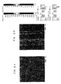
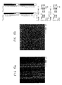
- the surface of the lead frame of the comparative example having many partial discoloured regions was observed by scanning electron microscope (JSM-T300, made by Japan Electron Optics Laboratory & Co., Ltd.; accelerated voltage 10KV, magnification 56.25 on the photograph).
- Fig. 2 shows the results of the observation of a comparative example as a typical figure showing the surface of a lead frame by scanning electron microphotograph.
- the partial discoloured region, part A has whitish vertical lines in the centre.
- the partial discoloured region looks whitish by scanning electron microphotograph, since Zr on the surface is oxidized.
- Zr is easily oxidized in an air atmosphere because Zr is an active metal which reacts with oxygen.
- the Part A shaped line looks like a blackish line to the naked eye.
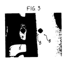
- Figure 3 is a microphotograph (x 32) of a comparative example. The figure shows that the surface of this comparative lead frame has plating scabs B caused by the heat treatment.
- the lead frame of the present invention As described above, according to the lead frame of the present invention, excellent surface conditions are obtained, making it possible to prevent the deterioration of the yield of production of IC, LSI and the like caused by defects on the surface of the lead frame. In addition, the lead frame according to the present invention remarkably contributes to the improvement of the reliability.
Landscapes
- Chemical & Material Sciences (AREA)
- Engineering & Computer Science (AREA)
- Materials Engineering (AREA)
- Mechanical Engineering (AREA)
- Metallurgy (AREA)
- Organic Chemistry (AREA)
- Lead Frames For Integrated Circuits (AREA)
- Conductive Materials (AREA)
Claims (9)
- Kupferlegierung, die 0,1 bis 1 Gew.% Chrom, 0,01 bis 0,5 Gew.% Zirconium und weniger als 0,005 Gew.% Schwefel enthält und teilweise verfärbte Bereiche aufweist, die durch das ungleichmäßige Anscheiden von Zirconium verursacht und darauf mit einer Dichte von 2 Körnern/100 cm² oder weniger verteilten Zirconiums verteilt sind, wobei der Rest abgesehen von Verunreinigungen Kupfer ist.
- Legierung nach Anspruch 1, die weniger als 0,05 Gew.% Eisen, weniger als 0,1 Gew.% Nickel, weniger als 0,05 Gew.% Phosphor, weniger als 0,1 Gew.% Zinn und weniger als 0,1 Gew.% Zink enthält.
- Legierung nach einem der vorhergehenden Ansprüche, deren Leitfähigkeit nicht weniger als 75IACS% beträgt.
- Leitergitter, das aus einer Kupferlegierung gemäß einem der vorhergehenden Ansprüchen hergestellt ist oder diese anderweitig aufweist.
- Leitergitter nach Anspruch 4, bei dem abblätternde Teile auf der Oberfläche des Leitergitters 5 Körner/Wicklung nicht überschreiten.
- Leitergitter nach Anspruch 4 oder 5, das durch Wärmebehandlung verursacht einen oder weniger Metallisierungsdefekte aufweist.
- Leitergitter nach einem der Ansprüche 4 bis 6, dessen Vickers-Härte nicht weniger als 150 Hv beträgt.
- Integrierte Schaltkreiskomponente oder LSI-Komponente, die ein Leitergitter gemäß einem der Ansprüche 4 bis 7 einbezieht.
- Verwendung einer Kupferlegierung nach einem der Ansprüche 1 bis 3 zur Herstellung von Leitergittern.
Applications Claiming Priority (2)
| Application Number | Priority Date | Filing Date | Title |
|---|---|---|---|
| JP404416/90 | 1990-12-20 | ||
| JP40441690 | 1990-12-20 |
Publications (2)
| Publication Number | Publication Date |
|---|---|
| EP0492987A1 EP0492987A1 (de) | 1992-07-01 |
| EP0492987B1 true EP0492987B1 (de) | 1995-06-14 |
Family
ID=18514092
Family Applications (1)
| Application Number | Title | Priority Date | Filing Date |
|---|---|---|---|
| EP91311805A Expired - Lifetime EP0492987B1 (de) | 1990-12-20 | 1991-12-19 | Kupferlegierungen und daraus hergestellte Leitergitter |
Country Status (4)
| Country | Link |
|---|---|
| US (2) | US5210441A (de) |
| EP (1) | EP0492987B1 (de) |
| KR (1) | KR960000710B1 (de) |
| DE (1) | DE69110435T2 (de) |
Families Citing this family (13)
| Publication number | Priority date | Publication date | Assignee | Title |
|---|---|---|---|---|
| EP0492987B1 (de) * | 1990-12-20 | 1995-06-14 | Kabushiki Kaisha Toshiba | Kupferlegierungen und daraus hergestellte Leitergitter |
| US5486244A (en) * | 1992-11-04 | 1996-01-23 | Olin Corporation | Process for improving the bend formability of copper alloys |
| WO1995025148A1 (en) * | 1994-03-17 | 1995-09-21 | Hitachi Maxell, Ltd. | Phosphor, phosphor composition, fluorescent mark carrier, and optical character reader |
| GB2311297B (en) * | 1994-03-22 | 1998-09-16 | Nippon Mining Co | Copper alloy suited for electrical components and having high strength and high electric conductivity |
| KR0175968B1 (ko) * | 1994-03-22 | 1999-02-18 | 코오노 히로노리 | 전자기기용 고강도고도전성 구리합금 |
| JP4130593B2 (ja) * | 2003-01-23 | 2008-08-06 | 日鉱金属株式会社 | 疲労及び中間温度特性に優れた高力高導電性銅合金 |
| JP2010045140A (ja) * | 2008-08-11 | 2010-02-25 | Nec Electronics Corp | リードフレーム、リードフレームの製造方法及び半導体装置の製造方法 |
| CN100587091C (zh) * | 2008-09-12 | 2010-02-03 | 邢台鑫晖铜业特种线材有限公司 | 接触线用Cu-Cr-Zr合金制备工艺 |
| JP5834528B2 (ja) * | 2011-06-22 | 2015-12-24 | 三菱マテリアル株式会社 | 電気・電子機器用銅合金 |
| CN104342575B (zh) * | 2014-10-11 | 2017-01-18 | 烟台万隆真空冶金股份有限公司 | 一种电气化铁路铬锆铜接触线及其加工工艺 |
| JP6990907B2 (ja) * | 2017-08-08 | 2022-02-03 | 三芳合金工業株式会社 | クロムジルコニウム銅合金鍛造板材及びその製造方法 |
| JP7035478B2 (ja) * | 2017-11-21 | 2022-03-15 | 三菱マテリアル株式会社 | 鋳造用モールド材 |
| US20220119919A1 (en) * | 2019-02-20 | 2022-04-21 | Mitsubishi Materials Corporation | Copper alloy material, commutator segment, and electrode material |
Family Cites Families (10)
| Publication number | Priority date | Publication date | Assignee | Title |
|---|---|---|---|---|
| JPS5620136A (en) * | 1979-07-30 | 1981-02-25 | Toshiba Corp | Copper alloy member |
| JPS58141544A (ja) * | 1982-02-17 | 1983-08-22 | Toshiba Corp | 電子部品 |
| JPS59117144A (ja) * | 1982-12-23 | 1984-07-06 | Toshiba Corp | リ−ドフレ−ムおよびその製造方法 |
| JPS59159243A (ja) * | 1983-03-02 | 1984-09-08 | Hitachi Ltd | 鋳造用金型 |
| JPS59193233A (ja) * | 1983-04-15 | 1984-11-01 | Toshiba Corp | 銅合金 |
| JPH0669076B2 (ja) * | 1985-06-28 | 1994-08-31 | 株式会社東芝 | リ−ドフレ−ム |
| DE3527341C1 (de) * | 1985-07-31 | 1986-10-23 | Wieland-Werke Ag, 7900 Ulm | Kupfer-Chrom-Titan-Silizium-Legierung und ihre Verwendung |
| US4749548A (en) * | 1985-09-13 | 1988-06-07 | Mitsubishi Kinzoku Kabushiki Kaisha | Copper alloy lead material for use in semiconductor device |
| JPH0775252B2 (ja) * | 1988-01-26 | 1995-08-09 | 三菱伸銅株式会社 | リードフレーム材の製造方法 |
| EP0492987B1 (de) * | 1990-12-20 | 1995-06-14 | Kabushiki Kaisha Toshiba | Kupferlegierungen und daraus hergestellte Leitergitter |
-
1991
- 1991-12-19 EP EP91311805A patent/EP0492987B1/de not_active Expired - Lifetime
- 1991-12-19 DE DE69110435T patent/DE69110435T2/de not_active Expired - Fee Related
- 1991-12-20 KR KR1019910023756A patent/KR960000710B1/ko not_active Expired - Fee Related
- 1991-12-20 US US07/810,426 patent/US5210441A/en not_active Expired - Lifetime
-
1993
- 1993-03-23 US US08/035,806 patent/US5341025A/en not_active Expired - Lifetime
Also Published As
| Publication number | Publication date |
|---|---|
| KR920013691A (ko) | 1992-07-29 |
| EP0492987A1 (de) | 1992-07-01 |
| US5210441A (en) | 1993-05-11 |
| DE69110435T2 (de) | 1995-11-16 |
| US5341025A (en) | 1994-08-23 |
| DE69110435D1 (de) | 1995-07-20 |
| KR960000710B1 (ko) | 1996-01-11 |
Similar Documents
| Publication | Publication Date | Title |
|---|---|---|
| EP0949343B1 (de) | Bleche aus Kupferlegierung für Elektronikbauteile | |
| KR100642571B1 (ko) | 피로특성이 우수한 Cu-Ni-Si계 합금 | |
| EP1801249B1 (de) | Kupferlegierung mit exzellenten Spannungsrelaxationseigenschaften | |
| US5210441A (en) | Lead frame formed of a copper-zirconium alloy | |
| WO2009096314A1 (ja) | 耐応力緩和特性に優れた銅合金板 | |
| EP2042613A1 (de) | Auf kupfer basierende walzlegierung und herstellungsverfahren dafür | |
| US6558617B2 (en) | Copper alloy for use in electric and electronic parts | |
| US5021105A (en) | Copper alloy for electronic instruments | |
| EP0114338B2 (de) | Leitergitter und Verfahren zu ihrer Herstellung | |
| EP1803829A1 (de) | Kupferlegierungsplatte für elektro- und elektronikteile mit biegebearbeitbarkeit | |
| US11746397B2 (en) | Palladium-copper-silver-ruthenium alloy | |
| JP4168077B2 (ja) | 酸化膜密着性に優れた電気電子部品用銅合金板 | |
| EP4116450A1 (de) | Reine kupferplatte, kupfer-/keramikverbundkörper und isolierte leiterplatte | |
| US6136104A (en) | Copper alloy for terminals and connectors and method for making same | |
| JP3797736B2 (ja) | 剪断加工性に優れる高強度銅合金 | |
| JPS63109130A (ja) | 電子機器用銅合金 | |
| JP5123720B2 (ja) | 耐熱性に優れた電気電子部品用銅合金板 | |
| WO2025225600A1 (ja) | Ag-Pd-Cu系合金からなるプローブピン用材料及びプローブピン | |
| US20230273240A1 (en) | Palladium-copper-silver alloy | |
| KR100238957B1 (ko) | 전기 전자부품용 구리합금 | |
| JPS63317636A (ja) | 半導体機器のバ−ンインicソケット用銅合金 | |
| JPH0593230A (ja) | リードフレーム材 | |
| EP0707084B1 (de) | Hochfeste beryllium-kupfer-legierung mit guter bearbeitbarkeit und wärmebeständigkeit und deren herstellung | |
| JP3779830B2 (ja) | 半導体リードフレーム用銅合金 | |
| JP2000038628A (ja) | 半導体リードフレーム用銅合金 |
Legal Events
| Date | Code | Title | Description |
|---|---|---|---|
| PUAI | Public reference made under article 153(3) epc to a published international application that has entered the european phase |
Free format text: ORIGINAL CODE: 0009012 |
|
| 17P | Request for examination filed |
Effective date: 19920110 |
|
| AK | Designated contracting states |
Kind code of ref document: A1 Designated state(s): DE FR GB |
|
| 17Q | First examination report despatched |
Effective date: 19940816 |
|
| GRAA | (expected) grant |
Free format text: ORIGINAL CODE: 0009210 |
|
| AK | Designated contracting states |
Kind code of ref document: B1 Designated state(s): DE FR GB |
|
| ET | Fr: translation filed | ||
| REF | Corresponds to: |
Ref document number: 69110435 Country of ref document: DE Date of ref document: 19950720 |
|
| PLBE | No opposition filed within time limit |
Free format text: ORIGINAL CODE: 0009261 |
|
| STAA | Information on the status of an ep patent application or granted ep patent |
Free format text: STATUS: NO OPPOSITION FILED WITHIN TIME LIMIT |
|
| 26N | No opposition filed | ||
| REG | Reference to a national code |
Ref country code: GB Ref legal event code: 746 Effective date: 19980929 |
|
| REG | Reference to a national code |
Ref country code: FR Ref legal event code: D6 |
|
| REG | Reference to a national code |
Ref country code: GB Ref legal event code: IF02 |
|
| PGFP | Annual fee paid to national office [announced via postgrant information from national office to epo] |
Ref country code: FR Payment date: 20021210 Year of fee payment: 12 |
|
| PGFP | Annual fee paid to national office [announced via postgrant information from national office to epo] |
Ref country code: GB Payment date: 20021218 Year of fee payment: 12 |
|
| PGFP | Annual fee paid to national office [announced via postgrant information from national office to epo] |
Ref country code: DE Payment date: 20021219 Year of fee payment: 12 |
|
| PG25 | Lapsed in a contracting state [announced via postgrant information from national office to epo] |
Ref country code: GB Free format text: LAPSE BECAUSE OF NON-PAYMENT OF DUE FEES Effective date: 20031219 |
|
| PG25 | Lapsed in a contracting state [announced via postgrant information from national office to epo] |
Ref country code: DE Free format text: LAPSE BECAUSE OF NON-PAYMENT OF DUE FEES Effective date: 20040701 |
|
| GBPC | Gb: european patent ceased through non-payment of renewal fee |
Effective date: 20031219 |
|
| PG25 | Lapsed in a contracting state [announced via postgrant information from national office to epo] |
Ref country code: FR Free format text: LAPSE BECAUSE OF NON-PAYMENT OF DUE FEES Effective date: 20040831 |
|
| REG | Reference to a national code |
Ref country code: FR Ref legal event code: ST |