EP0494745A2 - Verfahren für die Ätzung und/oder Einebung eines mehrschichtigen Halbleitersubstrats - Google Patents
Verfahren für die Ätzung und/oder Einebung eines mehrschichtigen Halbleitersubstrats Download PDFInfo
- Publication number
- EP0494745A2 EP0494745A2 EP92300080A EP92300080A EP0494745A2 EP 0494745 A2 EP0494745 A2 EP 0494745A2 EP 92300080 A EP92300080 A EP 92300080A EP 92300080 A EP92300080 A EP 92300080A EP 0494745 A2 EP0494745 A2 EP 0494745A2
- Authority
- EP
- European Patent Office
- Prior art keywords
- insulating film
- plasma gas
- semiconductor substrate
- ion etching
- layer
- Prior art date
- Legal status (The legal status is an assumption and is not a legal conclusion. Google has not performed a legal analysis and makes no representation as to the accuracy of the status listed.)
- Granted
Links
Images


Classifications
-
- H—ELECTRICITY
- H10—SEMICONDUCTOR DEVICES; ELECTRIC SOLID-STATE DEVICES NOT OTHERWISE PROVIDED FOR
- H10W—GENERIC PACKAGES, INTERCONNECTIONS, CONNECTORS OR OTHER CONSTRUCTIONAL DETAILS OF DEVICES COVERED BY CLASS H10
- H10W20/00—Interconnections in chips, wafers or substrates
- H10W20/01—Manufacture or treatment
- H10W20/071—Manufacture or treatment of dielectric parts thereof
- H10W20/092—Manufacture or treatment of dielectric parts thereof by smoothing the dielectric parts
-
- H—ELECTRICITY
- H10—SEMICONDUCTOR DEVICES; ELECTRIC SOLID-STATE DEVICES NOT OTHERWISE PROVIDED FOR
- H10P—GENERIC PROCESSES OR APPARATUS FOR THE MANUFACTURE OR TREATMENT OF DEVICES COVERED BY CLASS H10
- H10P50/00—Etching of wafers, substrates or parts of devices
- H10P50/20—Dry etching; Plasma etching; Reactive-ion etching
- H10P50/28—Dry etching; Plasma etching; Reactive-ion etching of insulating materials
- H10P50/282—Dry etching; Plasma etching; Reactive-ion etching of insulating materials of inorganic materials
- H10P50/283—Dry etching; Plasma etching; Reactive-ion etching of insulating materials of inorganic materials by chemical means
-
- H—ELECTRICITY
- H10—SEMICONDUCTOR DEVICES; ELECTRIC SOLID-STATE DEVICES NOT OTHERWISE PROVIDED FOR
- H10P—GENERIC PROCESSES OR APPARATUS FOR THE MANUFACTURE OR TREATMENT OF DEVICES COVERED BY CLASS H10
- H10P95/00—Generic processes or apparatus for manufacture or treatments not covered by the other groups of this subclass
- H10P95/06—Planarisation of inorganic insulating materials
- H10P95/062—Planarisation of inorganic insulating materials involving a dielectric removal step
- H10P95/064—Planarisation of inorganic insulating materials involving a dielectric removal step the removal being chemical etching
Definitions
- the present invention relates to a method of etching laminated semiconductor devices, and more particularly to a method of leveling the laminated surface of a semiconductor substrate, thereby providing a leveled surface on which wiring conductors are to be attached.
- a silicon substrate 1 has aluminum wiring conductors 2 of different widths attached to its top surface.
- a relatively thick insulating film 10 is formed on the surface of the semiconductor substrate 1.
- a coating layer 11 is formed on the insulating film 10.
- the lamination on the silicon substrate 1 is subjected to ion etching, which is carefully conditioned so as to permit the eating-out of the different materials of the insulating and coating layers at a same rate.
- Fig.2b shows a section of the insulating film 10 thus labeled.
- This leveling method has following defects: first, the insulating film must be very thick, and thick enough to prevent undesired exposure of aluminum wiring conductors 2 when the insulating film is eaten out deeply at selected areas because the eating rate is liable to vary from place to place; second, the overlying coating layer must be very thick because otherwise, its contour would be similar to the underlying irregular contour of the insulating film 10, thus allowing uneven eating-out of the lamination on the substrate; third, the insulating film 10 remains so thick over aluminum conductors 2 that contact or through holes when made deep enough to reach such aluminum conductors 2 will he inevitably deep and large in size, thus sometimes preventing lead wires from reaching underlying conductors, and causing underside space between lead wires and surrounding hole to allow invasion of moisture in contact regions; fourth, the eating-out of the two different materials at same rate is very difficult; and fifth, the critical point at which the eating-out of the lamination must be stopped cannot be determined with accuracy, and therefore, it is most likely that the eating-out is stopped at a
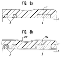
- a silicon substrate 1 has aluminum wiring conductors 2 attached to its surface and a relatively thick coating layer 11 formed on the surface of the semiconductor substrate 1 and the aluminum wiring conductors 2 thereon. Lest the coating layer 11 should be influenced by the underlying irregularity, the coating layer 11 must be thick enough for its upper surface to become substantially flat.
- the coating layer 11 is used as insulating layer to which other aluminum wiring conductors are to be attached. This insulating layer 11, however, is porous, allowing invasion of moisture to deteriorate the quality of insulation.
- porous layer 11 is sandwiched between lower and upper insulation films 12A and 12B. This, however, makes it difficult to make through holes, and the porous inner surface of the through hole surrounding the lead wire is exposed to the atmosphere, releasing the remaining volatile substance or moisture from the porous inner surface with the result that the quality of wiring connection is lowered.
- an object of the present invention to provide an etching method which can be used for levelling and a levelling method which permits the accurate controlling of etching of the lamination on a semiconductor substrate to provide a leveled surface on which wiring conductors may be fixed.
- the present invention provides a method of etching a surface of a laminated semiconductor substrate, which substrate includes a lower layer and an upper layer upon the lower layer, the upper layer being of a different material from said lower layer, the method comprising subjecting the upper layer to ion etching in a plasma gas atmosphere, detecting the exposure of part of the lower layer by sensing a sudden change in the amount of a constituent of said plasma gas atmosphere caused by said exposure, and controlling the ion etching in response thereto.
- the constituent of said plasma gas atmosphere is a gaseous reaction product resulting from a chemical reaction between the material of a said layer and an original constituent of the plasma gas atmosphere.
- the invention also provides a method of leveling a surface of a laminated semiconductor substrate comprising the steps of: preparing a semiconductor substrate having a plurality of wiring conductors attached thereto; forming a first insulating film on the surface of the semiconductor substrate and said wiring conductors; forming on said first insulating film, a second insulating film of a material which is different from the material of said first insulating film; forming a coating layer on said second insulating film; subjecting said coating layer to a first ion etching within a first plasma gas atmosphere; detecting the exposure of the part or parts of said second insulating film at its highest level from a sudden change in the amount of a gaseous reaction product resulting from a chemical reaction of the material of said coating layer with a selected constituent of the first plasma gas to stop said first ion etching; subjecting the etched surface to a second ion etching in a second plasma gas atmosphere, the rate at which the material of said second insulating film is eaten out being selected
- it further comprises the steps of: removing the remaining coating material from the upper surface of said second film; and forming an insulating film on said second film and the exposed part or parts of said first insulating film.
- said second ion etching is anisotropic.
- said second ion etching is isotropic
- the invention also includes a laminated semiconductor substrate having a surface levelled by a method according to the invention as set forth above.
- a semiconductor substrate 1 has a composite lamination on its upper surface. Specifically, aluminum wiring conductors of different widths 2 are attached to the upper surface of the semiconductor substrate 1; a first insulating film 3A of impurity-free silicon oxide is formed on the upper surface of the semiconductor substrate 1 and the aluminum wiring conductors 2; a second insulating film 4 of silicon oxide doped with phosphorus and boron (called “boron phosphrous silica glass, and abbreviated "BPSG”) is formed on the first insulating film 3A; and finally a coating layer 5 of novolak is formed on the second insulating film 4.
- BPSG boron phosphrous silica glass
- the first and second insulating films 3A and 4 may be formed one after another according to the plasma chemical vapor deposition process. Assume that the minimum space between adjacent conductors 2 is 800 nm and that conductors 2 are 500 nm thick. Then, the thickness of the first silicon oxide film 3A ranges from 100 to 300 nm, and the thickness of the second BPSG film 4 ranges from 300 to 800 nm. The individual thicknesses are so selected that the total thickness of these films may range from 500 to 700 nm.
- the surface of the second BPSG film 4 may be coated with a relatively low-viscous novolak resin such as commonly used as photoresist on the condition that a 500 nm-thick coating would result if it were a flat surface.
- the whole area of the resin coating layer 5 is subjected to an ion etching within oxygen plasma.
- the amount of the light of 451 nm wave length which is characteristic of carbon monoxide is monitored with the aid of a spectrometer to determine when the amount of the characteristic light decreases drastically; the ion etching is then stopped.
- the part or parts of the second insulating film 4 at its highest level have been exposed.
- the sudden decrease of the amount of reaction product, in this case a gas, in particular carbon monoxide, resulting from the chemical react ion of carbon in the resin of the coating layer 4 with the surrounding oxygen is attributable to removal of the coating resin from the peaks of the second insulating layer 4 and exposure of the peaks of the BPSG layer 4, which contains no carbon.
- the critical controling of the ion etching can be effected with ease and accuracy.
- the whole area of the remaining lamination is subjected to another ion etching within a mixture plasma of CF4+ CHF3 + Ar.
- the rate at which the material of the BPSG film 5 is eaten out is selected to be about two times larger than the rate at which the resin of the coating layer 5 is eaten out.
- the amount of the light of 451 nm wave length which is characteristic of carbon monoxide is monitored with the aid of a spectrometer to determine when the amount of the characteristic light increases drastically; the ion etching is then stopped, since there is now a substantially leveled surface with the peak or peaks of the first insulating film 3A exposed.
- the sudden increase of the amount of reaction product, in this case a gas, in particular carbon monoxide resulting from the chemical reaction of carbon in the surrounding gas with the silicon oxide of the first insulating film 3A indicates removal of the BPSG film from the peaks of the first insulating layer 3A and exposure of the peaks of the silicon oxide film 3A, which contains carbon.
- the critical controlling of the second ion etching can be effected with ease and accuracy, too.
- the remaining coating material 5 may be removed from the upper surface of the second film 4, and another silicon oxide film 3B may be formed on the second film 4 and the exposed peaks of the first insulating film 3A according to the plasma chemical vapor deposition process until the resulting insulating film 3B has been thick enough to provide good insulation between underlying and overlying wiring conductors 2 and 2′.
- the second ion etching is anisotropic, and therefore, the rising parts 6 of BPSG appear between the remaining coating material 5 and the second insulating film 4. Such rising parts 6 are minute and almost negligible from the point of leveling view. However, such rising parts 6 can be removed if the second ion etching is isotropic.
- the leveling method according to the present invention permits the critical controlling of the eating-out of selected materials in the composite lamination on a semiconductor substrate, thus assuring the reproducibility of leveled semiconductor substrate surface.
- the faster eating of the second film material has the effect of preventing appearance of the overlying coating irregularity on the leveled surface even if the coating layer is not thick.
- the eating amount is reduced compared with the conventional leveling methods, and accordingly the eating rate may remain constant over the whole area to be etched.
Landscapes
- Internal Circuitry In Semiconductor Integrated Circuit Devices (AREA)
- Drying Of Semiconductors (AREA)
Applications Claiming Priority (3)
| Application Number | Priority Date | Filing Date | Title |
|---|---|---|---|
| JP3000795A JPH0645327A (ja) | 1991-01-09 | 1991-01-09 | 半導体装置の製造方法 |
| JP795/91 | 1991-01-09 | ||
| JP79591 | 1991-01-09 |
Publications (3)
| Publication Number | Publication Date |
|---|---|
| EP0494745A2 true EP0494745A2 (de) | 1992-07-15 |
| EP0494745A3 EP0494745A3 (de) | 1994-03-16 |
| EP0494745B1 EP0494745B1 (de) | 1999-11-03 |
Family
ID=11483617
Family Applications (1)
| Application Number | Title | Priority Date | Filing Date |
|---|---|---|---|
| EP92300080A Expired - Lifetime EP0494745B1 (de) | 1991-01-09 | 1992-01-06 | Verfahren für die Ätzung und/oder Einebung eines mehrschichtigen Halbleitersubstrats |
Country Status (4)
| Country | Link |
|---|---|
| US (1) | US5272115A (de) |
| EP (1) | EP0494745B1 (de) |
| JP (1) | JPH0645327A (de) |
| DE (1) | DE69230229T2 (de) |
Cited By (3)
| Publication number | Priority date | Publication date | Assignee | Title |
|---|---|---|---|---|
| EP0688052A3 (de) * | 1994-05-20 | 1996-08-28 | Texas Instruments Inc | Verbesserungen in der oder in Bezug auf die Herstellung einer Halbleiteranordnung |
| WO1996026541A1 (en) * | 1995-02-21 | 1996-08-29 | Advanced Micro Devices, Inc. | Tunneling technology for reducing intra-conductive layer capacitance |
| EP0932191A1 (de) * | 1997-12-30 | 1999-07-28 | International Business Machines Corporation | Plasmaätzverfahren von dotierten Polysilizium Schichten mit gleichmässigen Ätzgeschwindigkeiten |
Families Citing this family (31)
| Publication number | Priority date | Publication date | Assignee | Title |
|---|---|---|---|---|
| US5384483A (en) * | 1992-02-28 | 1995-01-24 | Sgs-Thomson Microelectronics, Inc. | Planarizing glass layer spaced from via holes |
| JP2820187B2 (ja) * | 1992-04-16 | 1998-11-05 | 三星電子 株式会社 | 半導体装置の製造方法 |
| US5419803A (en) * | 1993-11-17 | 1995-05-30 | Hughes Aircraft Company | Method of planarizing microstructures |
| US5494854A (en) * | 1994-08-17 | 1996-02-27 | Texas Instruments Incorporated | Enhancement in throughput and planarity during CMP using a dielectric stack containing HDP-SiO2 films |
| US5672907A (en) * | 1995-03-22 | 1997-09-30 | Nippon Steel Corporation | Semiconductor device having character in BPSG film |
| US5814563A (en) * | 1996-04-29 | 1998-09-29 | Applied Materials, Inc. | Method for etching dielectric using fluorohydrocarbon gas, NH3 -generating gas, and carbon-oxygen gas |
| US5843847A (en) * | 1996-04-29 | 1998-12-01 | Applied Materials, Inc. | Method for etching dielectric layers with high selectivity and low microloading |
| KR100190048B1 (ko) * | 1996-06-25 | 1999-06-01 | 윤종용 | 반도체 소자의 소자 분리 방법 |
| US6115233A (en) * | 1996-06-28 | 2000-09-05 | Lsi Logic Corporation | Integrated circuit device having a capacitor with the dielectric peripheral region being greater than the dielectric central region |
| US6395620B1 (en) * | 1996-10-08 | 2002-05-28 | Micron Technology, Inc. | Method for forming a planar surface over low density field areas on a semiconductor wafer |
| US6108093A (en) * | 1997-06-04 | 2000-08-22 | Lsi Logic Corporation | Automated inspection system for residual metal after chemical-mechanical polishing |
| JPH1187286A (ja) | 1997-09-05 | 1999-03-30 | Lsi Logic Corp | 半導体ウエハの二段階式化学的機械的研磨方法及び装置 |
| US6234883B1 (en) | 1997-10-01 | 2001-05-22 | Lsi Logic Corporation | Method and apparatus for concurrent pad conditioning and wafer buff in chemical mechanical polishing |
| US6531397B1 (en) | 1998-01-09 | 2003-03-11 | Lsi Logic Corporation | Method and apparatus for using across wafer back pressure differentials to influence the performance of chemical mechanical polishing |
| US6060370A (en) * | 1998-06-16 | 2000-05-09 | Lsi Logic Corporation | Method for shallow trench isolations with chemical-mechanical polishing |
| US6241847B1 (en) | 1998-06-30 | 2001-06-05 | Lsi Logic Corporation | Method and apparatus for detecting a polishing endpoint based upon infrared signals |
| US6077783A (en) * | 1998-06-30 | 2000-06-20 | Lsi Logic Corporation | Method and apparatus for detecting a polishing endpoint based upon heat conducted through a semiconductor wafer |
| US6071818A (en) | 1998-06-30 | 2000-06-06 | Lsi Logic Corporation | Endpoint detection method and apparatus which utilize an endpoint polishing layer of catalyst material |
| US6268224B1 (en) | 1998-06-30 | 2001-07-31 | Lsi Logic Corporation | Method and apparatus for detecting an ion-implanted polishing endpoint layer within a semiconductor wafer |
| US6074517A (en) * | 1998-07-08 | 2000-06-13 | Lsi Logic Corporation | Method and apparatus for detecting an endpoint polishing layer by transmitting infrared light signals through a semiconductor wafer |
| US6285035B1 (en) | 1998-07-08 | 2001-09-04 | Lsi Logic Corporation | Apparatus for detecting an endpoint polishing layer of a semiconductor wafer having a wafer carrier with independent concentric sub-carriers and associated method |
| US6066266A (en) * | 1998-07-08 | 2000-05-23 | Lsi Logic Corporation | In-situ chemical-mechanical polishing slurry formulation for compensation of polish pad degradation |
| US6080670A (en) * | 1998-08-10 | 2000-06-27 | Lsi Logic Corporation | Method of detecting a polishing endpoint layer of a semiconductor wafer which includes a non-reactive reporting specie |
| US6201253B1 (en) | 1998-10-22 | 2001-03-13 | Lsi Logic Corporation | Method and apparatus for detecting a planarized outer layer of a semiconductor wafer with a confocal optical system |
| US6225210B1 (en) * | 1998-12-09 | 2001-05-01 | Advanced Micro Devices, Inc. | High density capping layers with improved adhesion to copper interconnects |
| US6121147A (en) * | 1998-12-11 | 2000-09-19 | Lsi Logic Corporation | Apparatus and method of detecting a polishing endpoint layer of a semiconductor wafer which includes a metallic reporting substance |
| US6117779A (en) | 1998-12-15 | 2000-09-12 | Lsi Logic Corporation | Endpoint detection method and apparatus which utilize a chelating agent to detect a polishing endpoint |
| US6528389B1 (en) | 1998-12-17 | 2003-03-04 | Lsi Logic Corporation | Substrate planarization with a chemical mechanical polishing stop layer |
| US7751609B1 (en) | 2000-04-20 | 2010-07-06 | Lsi Logic Corporation | Determination of film thickness during chemical mechanical polishing |
| KR100856325B1 (ko) * | 2005-12-29 | 2008-09-03 | 동부일렉트로닉스 주식회사 | 반도체 소자의 절연막 및 그 형성 방법 |
| US10879108B2 (en) * | 2016-11-15 | 2020-12-29 | Taiwan Semiconductor Manufacturing Co., Ltd. | Topographic planarization method for lithography process |
Family Cites Families (13)
| Publication number | Priority date | Publication date | Assignee | Title |
|---|---|---|---|---|
| JPS57102051A (en) * | 1980-12-17 | 1982-06-24 | Fujitsu Ltd | Manufacture of semiconductor device |
| JPS59147433A (ja) * | 1983-02-14 | 1984-08-23 | Hitachi Ltd | エツチング装置 |
| US4545852A (en) * | 1984-06-20 | 1985-10-08 | Hewlett-Packard Company | Planarization of dielectric films on integrated circuits |
| JPS61194748A (ja) * | 1985-02-25 | 1986-08-29 | Hitachi Ltd | 半導体集積回路装置の製造方法 |
| US4752129A (en) * | 1985-03-27 | 1988-06-21 | Anritsu Corporation | Wavelength modulation derivative spectrometer |
| JPS6273723A (ja) * | 1985-09-27 | 1987-04-04 | Sumitomo Electric Ind Ltd | エツチバツク法による平坦化工程終点検出方法 |
| JPS63107026A (ja) * | 1986-10-23 | 1988-05-12 | Tokuda Seisakusho Ltd | プラズマエツチング装置 |
| JPH0194623A (ja) * | 1987-10-06 | 1989-04-13 | Nec Corp | 多層配線半導体装置の製造方法 |
| GB2211348A (en) * | 1987-10-16 | 1989-06-28 | Philips Nv | A method of forming an interconnection between conductive levels |
| DE3801976A1 (de) * | 1988-01-23 | 1989-08-03 | Telefunken Electronic Gmbh | Verfahren zum planarisieren von halbleiteroberflaechen |
| GB2216336A (en) * | 1988-03-30 | 1989-10-04 | Philips Nv | Forming insulating layers on substrates |
| US4975141A (en) * | 1990-03-30 | 1990-12-04 | International Business Machines Corporation | Laser ablation for plasma etching endpoint detection |
| US5169491A (en) * | 1991-07-29 | 1992-12-08 | Micron Technology, Inc. | Method of etching SiO2 dielectric layers using chemical mechanical polishing techniques |
-
1991
- 1991-01-09 JP JP3000795A patent/JPH0645327A/ja active Pending
- 1991-12-30 US US07/816,035 patent/US5272115A/en not_active Expired - Fee Related
-
1992
- 1992-01-06 EP EP92300080A patent/EP0494745B1/de not_active Expired - Lifetime
- 1992-01-06 DE DE69230229T patent/DE69230229T2/de not_active Expired - Fee Related
Cited By (5)
| Publication number | Priority date | Publication date | Assignee | Title |
|---|---|---|---|---|
| EP0688052A3 (de) * | 1994-05-20 | 1996-08-28 | Texas Instruments Inc | Verbesserungen in der oder in Bezug auf die Herstellung einer Halbleiteranordnung |
| US5747880A (en) * | 1994-05-20 | 1998-05-05 | Texas Instruments Incorporated | Interconnect structure with an integrated low density dielectric |
| WO1996026541A1 (en) * | 1995-02-21 | 1996-08-29 | Advanced Micro Devices, Inc. | Tunneling technology for reducing intra-conductive layer capacitance |
| US5843836A (en) * | 1995-02-21 | 1998-12-01 | Advanced Micro Devices, Inc. | Tunneling technology for reducing intra-conductive layer capacitance |
| EP0932191A1 (de) * | 1997-12-30 | 1999-07-28 | International Business Machines Corporation | Plasmaätzverfahren von dotierten Polysilizium Schichten mit gleichmässigen Ätzgeschwindigkeiten |
Also Published As
| Publication number | Publication date |
|---|---|
| US5272115A (en) | 1993-12-21 |
| DE69230229T2 (de) | 2000-02-17 |
| DE69230229D1 (de) | 1999-12-09 |
| JPH0645327A (ja) | 1994-02-18 |
| EP0494745A3 (de) | 1994-03-16 |
| EP0494745B1 (de) | 1999-11-03 |
Similar Documents
| Publication | Publication Date | Title |
|---|---|---|
| EP0494745B1 (de) | Verfahren für die Ätzung und/oder Einebung eines mehrschichtigen Halbleitersubstrats | |
| KR930005949B1 (ko) | 반도체 디바이스 제조공정 | |
| US5458734A (en) | Method of fabricating a semiconductor device | |
| US7112542B2 (en) | Methods of forming materials between conductive electrical components, and insulating materials | |
| JPH0526337B2 (de) | ||
| US5654244A (en) | Process for producing semiconductor strain-sensitive sensor | |
| US5296094A (en) | Process for etching silicon dioxide layer without micro masking effect | |
| US6660624B2 (en) | Method for reducing fluorine induced defects on a bonding pad surface | |
| JPH10209128A (ja) | 平坦化終点検出方法 | |
| US5261998A (en) | Method for detecting an end point of etching in semiconductor manufacture using the emission spectrum of helium | |
| US6344364B1 (en) | Etching methods | |
| US4371890A (en) | Tapering of oxidized polysilicon electrodes | |
| JPH03194932A (ja) | 半導体装置の製造方法 | |
| JPH10189590A (ja) | 半導体装置及びその製造方法 | |
| US7294578B1 (en) | Use of a plasma source to form a layer during the formation of a semiconductor device | |
| JP2956627B2 (ja) | 不純物濃度分析方法 | |
| US6905893B1 (en) | Method and structure for determining a concentration profile of an impurity within a semiconductor layer | |
| JPH0334426A (ja) | 埋め込み酸化膜の形成方法 | |
| EP0936679A1 (de) | Verfahren zur Herstellung von Halbleitervorrichtungen mit eingebautem Kondensator | |
| JPH0744174B2 (ja) | エツチング方法 | |
| JP3225676B2 (ja) | 半導体装置の製造方法 | |
| JPH0982799A (ja) | 配線基板およびその製造方法 | |
| JPS62296425A (ja) | エツチバツク平坦化方法 | |
| JP2604350B2 (ja) | エッチング方法 | |
| US7365020B2 (en) | Method for etching upper metal of capacitator |
Legal Events
| Date | Code | Title | Description |
|---|---|---|---|
| PUAI | Public reference made under article 153(3) epc to a published international application that has entered the european phase |
Free format text: ORIGINAL CODE: 0009012 |
|
| 17P | Request for examination filed |
Effective date: 19920128 |
|
| AK | Designated contracting states |
Kind code of ref document: A2 Designated state(s): DE FR GB |
|
| PUAL | Search report despatched |
Free format text: ORIGINAL CODE: 0009013 |
|
| AK | Designated contracting states |
Kind code of ref document: A3 Designated state(s): DE FR GB |
|
| 17Q | First examination report despatched |
Effective date: 19950824 |
|
| GRAG | Despatch of communication of intention to grant |
Free format text: ORIGINAL CODE: EPIDOS AGRA |
|
| GRAG | Despatch of communication of intention to grant |
Free format text: ORIGINAL CODE: EPIDOS AGRA |
|
| GRAG | Despatch of communication of intention to grant |
Free format text: ORIGINAL CODE: EPIDOS AGRA |
|
| GRAH | Despatch of communication of intention to grant a patent |
Free format text: ORIGINAL CODE: EPIDOS IGRA |
|
| GRAH | Despatch of communication of intention to grant a patent |
Free format text: ORIGINAL CODE: EPIDOS IGRA |
|
| GRAA | (expected) grant |
Free format text: ORIGINAL CODE: 0009210 |
|
| AK | Designated contracting states |
Kind code of ref document: B1 Designated state(s): DE FR GB |
|
| REF | Corresponds to: |
Ref document number: 69230229 Country of ref document: DE Date of ref document: 19991209 |
|
| ET | Fr: translation filed | ||
| PLBE | No opposition filed within time limit |
Free format text: ORIGINAL CODE: 0009261 |
|
| 26N | No opposition filed | ||
| REG | Reference to a national code |
Ref country code: GB Ref legal event code: IF02 |
|
| PGFP | Annual fee paid to national office [announced via postgrant information from national office to epo] |
Ref country code: GB Payment date: 20020109 Year of fee payment: 11 |
|
| PGFP | Annual fee paid to national office [announced via postgrant information from national office to epo] |
Ref country code: FR Payment date: 20020110 Year of fee payment: 11 |
|
| PGFP | Annual fee paid to national office [announced via postgrant information from national office to epo] |
Ref country code: DE Payment date: 20020212 Year of fee payment: 11 |
|
| PG25 | Lapsed in a contracting state [announced via postgrant information from national office to epo] |
Ref country code: GB Free format text: LAPSE BECAUSE OF NON-PAYMENT OF DUE FEES Effective date: 20030106 |
|
| PG25 | Lapsed in a contracting state [announced via postgrant information from national office to epo] |
Ref country code: DE Free format text: LAPSE BECAUSE OF NON-PAYMENT OF DUE FEES Effective date: 20030801 |
|
| GBPC | Gb: european patent ceased through non-payment of renewal fee |
Effective date: 20030106 |
|
| PG25 | Lapsed in a contracting state [announced via postgrant information from national office to epo] |
Ref country code: FR Free format text: LAPSE BECAUSE OF NON-PAYMENT OF DUE FEES Effective date: 20030930 |
|
| REG | Reference to a national code |
Ref country code: FR Ref legal event code: ST |