EP0496443A1 - Halbleiteranordnung und Verfahren zum Herstellen einer derartigen Halbleiteranordnung - Google Patents
Halbleiteranordnung und Verfahren zum Herstellen einer derartigen Halbleiteranordnung Download PDFInfo
- Publication number
- EP0496443A1 EP0496443A1 EP92200079A EP92200079A EP0496443A1 EP 0496443 A1 EP0496443 A1 EP 0496443A1 EP 92200079 A EP92200079 A EP 92200079A EP 92200079 A EP92200079 A EP 92200079A EP 0496443 A1 EP0496443 A1 EP 0496443A1
- Authority
- EP
- European Patent Office
- Prior art keywords
- layer
- insulating layer
- etching stopper
- conductive regions
- etching
- Prior art date
- Legal status (The legal status is an assumption and is not a legal conclusion. Google has not performed a legal analysis and makes no representation as to the accuracy of the status listed.)
- Granted
Links
Images

Classifications
-
- H—ELECTRICITY
- H10—SEMICONDUCTOR DEVICES; ELECTRIC SOLID-STATE DEVICES NOT OTHERWISE PROVIDED FOR
- H10D—INORGANIC ELECTRIC SEMICONDUCTOR DEVICES
- H10D48/00—Individual devices not covered by groups H10D1/00 - H10D44/00
- H10D48/30—Devices controlled by electric currents or voltages
- H10D48/32—Devices controlled by only the electric current supplied, or only the electric potential applied, to an electrode which does not carry the current to be rectified, amplified or switched
-
- H—ELECTRICITY
- H10—SEMICONDUCTOR DEVICES; ELECTRIC SOLID-STATE DEVICES NOT OTHERWISE PROVIDED FOR
- H10W—GENERIC PACKAGES, INTERCONNECTIONS, CONNECTORS OR OTHER CONSTRUCTIONAL DETAILS OF DEVICES COVERED BY CLASS H10
- H10W20/00—Interconnections in chips, wafers or substrates
- H10W20/01—Manufacture or treatment
- H10W20/071—Manufacture or treatment of dielectric parts thereof
- H10W20/081—Manufacture or treatment of dielectric parts thereof by forming openings in the dielectric parts
- H10W20/084—Manufacture or treatment of dielectric parts thereof by forming openings in the dielectric parts for dual-damascene structures
- H10W20/086—Manufacture or treatment of dielectric parts thereof by forming openings in the dielectric parts for dual-damascene structures involving buried masks
-
- H—ELECTRICITY
- H10—SEMICONDUCTOR DEVICES; ELECTRIC SOLID-STATE DEVICES NOT OTHERWISE PROVIDED FOR
- H10D—INORGANIC ELECTRIC SEMICONDUCTOR DEVICES
- H10D44/00—Charge transfer devices
- H10D44/01—Manufacture or treatment
- H10D44/041—Manufacture or treatment having insulated gates
-
- H—ELECTRICITY
- H10—SEMICONDUCTOR DEVICES; ELECTRIC SOLID-STATE DEVICES NOT OTHERWISE PROVIDED FOR
- H10F—INORGANIC SEMICONDUCTOR DEVICES SENSITIVE TO INFRARED RADIATION, LIGHT, ELECTROMAGNETIC RADIATION OF SHORTER WAVELENGTH OR CORPUSCULAR RADIATION
- H10F39/00—Integrated devices, or assemblies of multiple devices, comprising at least one element covered by group H10F30/00, e.g. radiation detectors comprising photodiode arrays
- H10F39/10—Integrated devices
- H10F39/12—Image sensors
- H10F39/15—Charge-coupled device [CCD] image sensors
- H10F39/153—Two-dimensional or three-dimensional array CCD image sensors
- H10F39/1536—Frame transfer
-
- H—ELECTRICITY
- H10—SEMICONDUCTOR DEVICES; ELECTRIC SOLID-STATE DEVICES NOT OTHERWISE PROVIDED FOR
- H10F—INORGANIC SEMICONDUCTOR DEVICES SENSITIVE TO INFRARED RADIATION, LIGHT, ELECTROMAGNETIC RADIATION OF SHORTER WAVELENGTH OR CORPUSCULAR RADIATION
- H10F39/00—Integrated devices, or assemblies of multiple devices, comprising at least one element covered by group H10F30/00, e.g. radiation detectors comprising photodiode arrays
- H10F39/80—Constructional details of image sensors
-
- H—ELECTRICITY
- H10—SEMICONDUCTOR DEVICES; ELECTRIC SOLID-STATE DEVICES NOT OTHERWISE PROVIDED FOR
- H10W—GENERIC PACKAGES, INTERCONNECTIONS, CONNECTORS OR OTHER CONSTRUCTIONAL DETAILS OF DEVICES COVERED BY CLASS H10
- H10W20/00—Interconnections in chips, wafers or substrates
- H10W20/01—Manufacture or treatment
-
- Y—GENERAL TAGGING OF NEW TECHNOLOGICAL DEVELOPMENTS; GENERAL TAGGING OF CROSS-SECTIONAL TECHNOLOGIES SPANNING OVER SEVERAL SECTIONS OF THE IPC; TECHNICAL SUBJECTS COVERED BY FORMER USPC CROSS-REFERENCE ART COLLECTIONS [XRACs] AND DIGESTS
- Y10—TECHNICAL SUBJECTS COVERED BY FORMER USPC
- Y10S—TECHNICAL SUBJECTS COVERED BY FORMER USPC CROSS-REFERENCE ART COLLECTIONS [XRACs] AND DIGESTS
- Y10S438/00—Semiconductor device manufacturing: process
- Y10S438/97—Specified etch stop material
Definitions
- the invention relates to a semiconductor device comprising a semiconductor body having at a surface one or several circuit elements with at least two conductive regions, the surface being coated with an insulating layer on which a conductor track is provided which interconnects the conductive regions through contact windows in the insulating layer and which is recessed into the insulating layer over at least substantially its entire thickness.
- the invention also relates to a method of manufacturing a semiconductor device comprising a semiconductor body having at a surface one or several circuit elements with at least two conductive regions, the surface being coated with an insulating layer on which a conductor track is formed which interconnects the conductive regions through contact windows in the insulating layer and which is recessed into the insulating layer over at least substantially its entire thickness.
- conductive regions is to be widely interpreted here so as to include: doped semiconductor zones in the semiconductor body, gate electrodes of field effect devices, portions of subjacent wirings, contact surfaces, etc.
- the interconnection pattern lies recessed in the insulating layer, so that the structure remains plane.
- no plugs are required for the connections between the interconnection pattern and semiconductor zones or poly tracks.
- a semiconductor device of the kind described in the opening paragraph according to the invention is characterized in that an etching stopper layer is present in an interposed region between the conductive regions, which layer separates the conductor track from a subjacent portion of the insulating layer and which comprises a material which is selectively etchable relative to the insulating layer, while the etching stopper layer forms part of a layer pattern manufactured from a common layer, which pattern comprises besides the etching stopper layer further portions elsewhere in the device.
- a polycrystalline silicon layer for example, or a dielectric layer of a material different from the insulating layer may be used for the etching stopper layer. Since such a layer is usually present in the process anyway, it is not necessary to use a separate photomask for the contact windows.
- a method of the kind described in the opening paragraph is characterized in that, after the conductive regions have been provided, the insulating layer is formed over a first part of its thickness, in that an etching stopper layer of a conductive material which is selectively etchable relative to the insulating layer is formed on this part in an intermediate region situated between the conductive regions, and in that subsequently the insulating layer is provided over a second part of its thickness, upon which the insulating layer is subjected to an etching treatment at the area of the conductor track to be formed, during which it is removed in the said intermediate region down to the etching stopper layer and at the area of the contact windows down to the conductive regions, after which the configuration thus obtained is covered with a conductive layer, from which the recessed conductor track is formed by etching back.
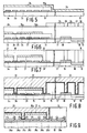
- Fig. 1 shows a diagrammatic plan view of a raster transfer imaging device comprising a system of vertical CCD lines 1 situated next to one another divided into an imaging section A and a memory section B.
- the imaging section A serves, as is known, for converting a projected image into charge packages.
- these charge packages are quickly transported to the memory section B which is screened from incident radiation.
- the horizontal readout register C which is provided with an output amplifier 2.
- the charge packages stored in the B section are transported to the readout register C row by row and read sequentially at the output amplifier 2.
- the charge transport and charge storage are controlled by clock voltages which are applied to clock electrodes 3, four of which are diagrammatically depicted in Fig. 1, ⁇ 1, ⁇ 2, ⁇ 3 and ⁇ 4.
- the clock electrodes are made by the double- or triple-layer poly-Si technology, by means of which an overlapping gate structure is made in two or three layers.
- a drawback of this technology is that the structure onto which the image is projected is of very imperfect flatness, so that light can be deflected towards insensitive regions.
- the poly layers used are usually 0,3-0,5 ⁇ m thick, which is too thick for transmitting sufficient blue light. Therefore, a photosensitive surface free from poly-Si is often formed through adaptation of the gate configuration. The thickness of the poly-Si is so great because otherwise, i.e.
- a single-layer poly technology will be used for the clock electrodes of at least the A section with a very thin poly layer, approximately 50 nm thick, so that the sensor has a good sensitivity to the entire visible spectrum, there is no overlap between the gates of the various phases, and the structure is topographically very plane.
- Fig. 2 is a diagrammatic plan view of part of the electrode configuration in the imaging section A.
- the clock electrodes 3 are formed by non-overlapping polystrips with a thickness of 50 nm situated next to one another.
- the comparatively high-ohmic tracks 3 are connected to low-ohmic metal tracks 4 which are connected to the polystrips 3 at the areas of the dots.
- each metal strip 4 is connected to each fourth clock electrode 3.
- the metal strips 4 may be made very narrow, so that comparatively wide spaces remain open between the metal strips, through which spaces the light may penetrate into the semiconductor body.
- the gates 3 may each be connected to the clock lines by a number of interspaced tracks 4 in order to obtain the desired low RC time value.
- the metal tracks 4 may be connected to four clock lines 5, by means of which the clocks ⁇ 1, ⁇ 2, ⁇ 3 and ⁇ 4 are provided, via connections 6.
- Fig. 3a shows in cross-section a portion of a semiconductor device in which the invention is incorporated, with a portion of a charge-coupled device to be used in the imaging section A of the imaging device according to Fig. 2, and an MOS transistor which is integrated with the charge-coupled device.
- Fig. 3b gives a diagrammatic plan view of the portion shown in Fig. 3a.
- the device comprises a semiconductor body 10 of silicon with a surface 11 at which or near which the charge-coupled device 12 and the MOST 13 are situated.
- the charge-coupled device comprises a range of clock electrodes 3a, 3b, 3c, etc. formed by thin, approximately 50 nm thick polycrystalline silicon tracks.
- the gates 3 constitute the conductive regions referred to above and are separated from the surface 11 by the thin dielectric layer 14.
- the gate dielectric only comprises a silicon oxide layer, but it may obviously also consist of a different insulating material or of double layers of, for example, silicon oxide and silicon nitride.
- the gates 3 are embedded in a dielectric layer 15 which may be entirely of silicon oxide, but which may obviously also be composed entirely or partly of other materials.
- the layer 15 is composed of two portions 15a and 15b, which will be discussed below.
- the MOS transistor 13 comprises a source and a drain zone 17, 18 and a gate electrode 19 which is insulated from the subjacent channel region by the gate oxide 14.
- a conductor track 4 is formed which interconnects the conductive regions 3b and 3f via contact windows in the insulating layer 15.
- the conductor 4 is embedded in the layer 15 over at least substantially its entire thickness, so that a practically plane upper surface is obtained.
- an etching stopper layer 21 separating the conductor track 4 from the subjacent portion 15a of the insulating layer 15 is present in the intermediate region between the conductive regions 3b and 3f.
- the layer 21 comprises a material which is different from that of the insulating layer 15 and relative to which the layer 15 can be selectively etched.
- the etching stopper layer 21 requires no extra process steps since the layer 21 forms part of a layer pattern manufactured from a common layer, which pattern comprises besides the etching stopper layer 21 further portions in the device and which can accordingly be formed simultaneously with these further portions.
- the etching stopper layer 21 is made of polycrystalline silicon which together with the gate 19 of the transistor 13 belongs to the second polycrystalline wiring layer.
- the thickness of this second layer is approximately 0,4 ⁇ m and is chosen to be much greater, for reasons of resistance, than the thickness of the gates 3a, 3b, etc. which is only approximately 50 nm for reasons of photosensitivity.
- the transistor 13 is further provided with a contact 22 which is connected to the zone 18, and with a contact 23 which is connected to the gate 19, the contacts 22, 23 being formed by plugs.
- the contact 23 is drawn above the channel region in the drawing. In actual fact, however, it will preferably be provided above the field oxide not shown in the drawing.
- Fig. 5 shows the stage in which the clock electrodes 3 are formed from an approximately 50 nm thick polycrystalline silicon layer.
- the gates 3 are then coated with an oxide layer 15a.
- This layer which may be provided by, for example, CVD techniques known per se and local removal through etching, has a thickness of approximately 0,3 ⁇ m. Then an approximately 0,4 ⁇ m thick second polycrystalline silicon layer 24 is provided by deposition.
- the gate 19 of the MOST 13 is formed from this layer, and on the other hand the etching stopper layer 21.
- the width of the etching stopper layer is 1,7 - 2 ⁇ m and is chosen to be somewhat greater than the width of the conductor track 4 to be provided in a later stage.
- the layer 21 has an interruption with a width of approximately 1,1 ⁇ m at the area of the connection to be provided between the conductor track 4 and the gate 3b, at a width of approximately 2 ⁇ m of the gate 3b.
- the entire assembly is then covered with a thick oxide layer 15b, having a thickness of approximately 1 ⁇ m.
- a mask 26 in the form of a photoresist layer is formed on the surface of this oxide layer, which mask is complementary to, or the inverted image of, the metal pattern to be obtained at a later stage.
- the mask 26 has openings 27 at the areas of the contacts 22, 23 and an opening 28 at the area of the connection 4 to be formed.
- the width of the opening 28, which is situated as symmetrically as possible above the etching stopper layer 21, is approximately 1,1 ⁇ m, so that the etching stopper layer projects by approximately 0,3-0,5 ⁇ m on either side of the opening 28.
- the source and drain zones 17, 18 of MOSTs and other zones may also be provided.
- the device is then in the stage as shown in Fig. 6. Then the device is subjected to an etching treatment during which the oxide layer 15a, 15b is removed at the areas of the openings 27, 28.
- the etching treatment is carried out selectively in that the polycrystalline silicon of the gates 3, 19 and the etching stopper layer 21 are not attacked or at least attacked to a much lesser degree during etching of the oxide.
- Etching is preferably carried out in an anisotropic plasma etching stage to prevent underetching.
- Etching of the oxide is continued down to a depth where a different material is present, i.e. for example up to the monocrystalline Si material at the area of the source or drain zone 18, down to the polycrystalline Si material at the area of the gate 19 of the MOST and the etching stopper layer 21.
- the contact window 30 is formed at the area of the gate 3b, where the etching stopper layer 21 has an interruption 25.
- Etching of the oxide layer 15 continues down to the polycrystalline Si material of the first poly layer.
- the width of the window 30 in the direction of the cross-section of Fig. 7 is determined by the width of the interruption 25 in the etching stopper layer 21.
- the width in the direction transverse to the plane of the drawing is determined by the mask 26.
- the width of the contact window 31 at the area of the poly track 3f is determined, in the cross-section of Fig. 7, by the spacing between the etching stopper layer 21 to the left of the window 31 and the edge of the mask 26 to the right of the window 31 to be formed.
- the width of the window 31 in the direction transverse to the plane of the drawing is again determined by the mask 26.
- a thick metal layer 31 (Fig. 8) is provided, which covers the entire surface.
- Tungsten is chosen for the layer 32 in the present embodiment. Obviously, other suitable materials may also be chosen.
- a thin layer of TiW 33 may be provided, for example, by sputtering. The layer 33 ensures a good adhesion of the metal layer 32 and also forms a good barrier against diffusion.
- the metal layer 32/33 is subjected to an etching treatment and etched back to the upper surface of the thick oxide layer 15.
- the configuration of Fig. 3 is then obtained.
- the use of the second polycrystalline silicon layer for the etching stopper layer 21 renders an extra mask for masking the oxide layer 15 in the intermediate region between the contact windows 30, 31 to be formed redundant.
- Only two polycrystalline silicon layers are used in the embodiment described here.
- Fig. 9 gives in cross-section an embodiment comprising three polycrystalline layers. Only part of a CCD channel is shown in the drawing.
- the charge-coupled device comprises clock electrodes in two poly layers, i.e. the gates 35a, b, c in poly 1, and the gates 36a, b, c in poly 2.
- the thickness of the two poly layers is between, for example, 0,3 and 0,5 ⁇ m. This thickness is much greater than the thickness of the CCD electrodes 3 in the preceding embodiment, so that the resistance will be much lower. Nevertheless, it may yet be advantageous also in this case to connect the electrodes to low-ohmic bridge connections 4, for example, when the dimensions of the image sensor are very great.
- the electrodes 35a, 35b, 35c are formed from a first polycrystalline silicon layer, with openings between the electrodes.
- a second polycrystalline silicon layer is deposited, from which the gates 36a, 36b, 36c are formed, which fill up the openings between the gates 35.
- the gates 36 may overlap the gates 35, as is shown in Fig. 9.
- the gates 35, 36 are covered with the oxide layer 15a, after which a third polycrystalline silicon layer is deposited, from which the etching stopper layer 21 is formed. Since this third polylayer is necessary elsewhere in any case, inter alia for the parallel-serial interface (not shown in Fig.
- the provision of the etching stopper layer 21 does not require an extra deposition step and mask.
- the gate electrode 19 of MOS transistors may be formed in poly 2 before doping stages for source and drain zones are implemented.
- the manufacture of the device can be continued in a manner analogous to that for the preceding embodiment.
- a thick oxide layer 15 is then deposited first, in which the pattern of the wiring to be shaped is provided by means of an inverted metal mask. Etching continues at the areas of the gates 35b and 35d down to the polymaterial of these gates. In the area situated between these gates, etching is stopped by the etching stopper layer 21. After the etching treatment, the recessed metal pattern with the bridge connection 4 is formed in the manner described above by means of deposition and etching back.
- etching stopper layer 21 need not necessarily consist of polysilicon, it may alternatively consist of a different material, for example, silicide. Instead of W or TiW, other metals or conductive materials, such as doped semiconductor material, may be used for the connections 4.
Landscapes
- Solid State Image Pick-Up Elements (AREA)
- Internal Circuitry In Semiconductor Integrated Circuit Devices (AREA)
- Drying Of Semiconductors (AREA)
Applications Claiming Priority (2)
| Application Number | Priority Date | Filing Date | Title |
|---|---|---|---|
| NL9100094 | 1991-01-21 | ||
| NL9100094A NL9100094A (nl) | 1991-01-21 | 1991-01-21 | Halfgeleiderinrichting en werkwijze ter vervaardiging van een dergelijke halfgeleiderinrichting. |
Publications (2)
| Publication Number | Publication Date |
|---|---|
| EP0496443A1 true EP0496443A1 (de) | 1992-07-29 |
| EP0496443B1 EP0496443B1 (de) | 1998-09-09 |
Family
ID=19858750
Family Applications (1)
| Application Number | Title | Priority Date | Filing Date |
|---|---|---|---|
| EP92200079A Expired - Lifetime EP0496443B1 (de) | 1991-01-21 | 1992-01-14 | Halbleiteranordnung und Verfahren zum Herstellen einer derartigen Halbleiteranordnung |
Country Status (6)
| Country | Link |
|---|---|
| US (2) | US5396092A (de) |
| EP (1) | EP0496443B1 (de) |
| JP (1) | JP3048459B2 (de) |
| KR (1) | KR100273070B1 (de) |
| DE (1) | DE69226887T2 (de) |
| NL (1) | NL9100094A (de) |
Cited By (5)
| Publication number | Priority date | Publication date | Assignee | Title |
|---|---|---|---|---|
| EP0625800A1 (de) * | 1993-05-21 | 1994-11-23 | Koninklijke Philips Electronics N.V. | Ladungsgekoppelte Bildaufnahmeanordnung |
| US5449931A (en) * | 1993-05-21 | 1995-09-12 | U.S. Philips Corporation | Charge coupled imaging device having multilayer gate electrode wiring |
| EP0766303A3 (de) * | 1995-09-29 | 1997-04-23 | Toshiba Kk | |
| US5652173A (en) * | 1996-05-09 | 1997-07-29 | Philips Electronics North America Corporation | Monolithic microwave circuit with thick conductors |
| EP0757380A3 (de) * | 1995-07-31 | 1997-12-29 | Eastman Kodak Company | Verfahren zur Herstellung einer planaren ladungsgekoppelten Anordnung mit seitlich ausgerichteten Implantierungen und durch deckenden metallverbundenen Elektroden |
Families Citing this family (12)
| Publication number | Priority date | Publication date | Assignee | Title |
|---|---|---|---|---|
| NL9100094A (nl) * | 1991-01-21 | 1992-08-17 | Koninkl Philips Electronics Nv | Halfgeleiderinrichting en werkwijze ter vervaardiging van een dergelijke halfgeleiderinrichting. |
| US5382545A (en) * | 1993-11-29 | 1995-01-17 | United Microelectronics Corporation | Interconnection process with self-aligned via plug |
| US5635421A (en) * | 1995-06-15 | 1997-06-03 | Taiwan Semiconductor Manufacturing Company | Method of making a precision capacitor array |
| US6008121A (en) * | 1996-03-19 | 1999-12-28 | Siemens Aktiengesellschaft | Etching high aspect contact holes in solid state devices |
| JPH09270461A (ja) * | 1996-03-29 | 1997-10-14 | Mitsubishi Electric Corp | 半導体装置 |
| EP0925604B1 (de) * | 1997-05-29 | 2008-07-09 | Nxp B.V. | Methode zur herstellung einer elektronischen schaltung, wobei eine leitetende schicht auf einer isolierenden schicht hergestellt wird und daraus ein leitungsmuster gemacht wird |
| US5989784A (en) * | 1998-04-06 | 1999-11-23 | Taiwan Semiconductor Manufacturing Company, Ltd. | Etch recipe for embedded DRAM passivation with etch stopping layer scheme |
| JP2004519857A (ja) * | 2001-03-21 | 2004-07-02 | コーニンクレッカ フィリップス エレクトロニクス エヌ ヴィ | タングステンプラグで相互接続されるメタライゼーション層を備える半導体デバイスの製造方法 |
| DE10320166B4 (de) * | 2002-05-16 | 2007-06-06 | Dalsa Corp., Waterloo | Pixelentwurf für CCD-Bildsensoren |
| US6562711B1 (en) * | 2002-06-28 | 2003-05-13 | Intel Corporation | Method of reducing capacitance of interconnect |
| US8166438B2 (en) * | 2009-01-28 | 2012-04-24 | Oracle America, Inc. | Low RC local clock distribution |
| US8245781B2 (en) * | 2009-12-11 | 2012-08-21 | Schlumberger Technology Corporation | Formation fluid sampling |
Citations (3)
| Publication number | Priority date | Publication date | Assignee | Title |
|---|---|---|---|---|
| EP0224013A2 (de) * | 1985-10-28 | 1987-06-03 | International Business Machines Corporation | Verfahren zur Herstellung koplanarer Viellagen-Metall-Isolator-Schichten auf einem Substrat |
| EP0272051A2 (de) * | 1986-12-17 | 1988-06-22 | Advanced Micro Devices, Inc. | Aneinandergefügte Kontaktstruktur mit vermindertem Flächenbedarf |
| US4808552A (en) * | 1985-09-11 | 1989-02-28 | Texas Instruments Incorporated | Process for making vertically-oriented interconnections for VLSI devices |
Family Cites Families (9)
| Publication number | Priority date | Publication date | Assignee | Title |
|---|---|---|---|---|
| US4163239A (en) * | 1971-12-30 | 1979-07-31 | Texas Instruments Incorporated | Second level phase lines for CCD line imager |
| US4291328A (en) * | 1979-06-15 | 1981-09-22 | Texas Instruments Incorporated | Interlevel insulator for integrated circuit with implanted resistor element in second-level polycrystalline silicon |
| US4488166A (en) * | 1980-12-09 | 1984-12-11 | Fairchild Camera & Instrument Corp. | Multilayer metal silicide interconnections for integrated circuits |
| JPS5966165A (ja) * | 1982-10-08 | 1984-04-14 | Hitachi Ltd | 電極配線およびその製造方法 |
| JPS601846A (ja) * | 1983-06-18 | 1985-01-08 | Toshiba Corp | 多層配線構造の半導体装置とその製造方法 |
| NL8501339A (nl) * | 1985-05-10 | 1986-12-01 | Philips Nv | Halfgeleiderinrichting en werkwijze ter vervaardiging daarvan. |
| JPS61280638A (ja) * | 1985-06-06 | 1986-12-11 | Toshiba Corp | 半導体装置の製造方法 |
| JPH02134992A (ja) * | 1988-11-15 | 1990-05-23 | Matsushita Electron Corp | 固体撮像素子 |
| NL9100094A (nl) * | 1991-01-21 | 1992-08-17 | Koninkl Philips Electronics Nv | Halfgeleiderinrichting en werkwijze ter vervaardiging van een dergelijke halfgeleiderinrichting. |
-
1991
- 1991-01-21 NL NL9100094A patent/NL9100094A/nl not_active Application Discontinuation
-
1992
- 1992-01-14 EP EP92200079A patent/EP0496443B1/de not_active Expired - Lifetime
- 1992-01-14 DE DE69226887T patent/DE69226887T2/de not_active Expired - Fee Related
- 1992-01-18 KR KR1019920000667A patent/KR100273070B1/ko not_active Expired - Fee Related
- 1992-01-21 JP JP4008554A patent/JP3048459B2/ja not_active Expired - Fee Related
-
1994
- 1994-04-08 US US08/225,403 patent/US5396092A/en not_active Expired - Fee Related
- 1994-11-29 US US08/346,947 patent/US5536678A/en not_active Expired - Fee Related
Patent Citations (3)
| Publication number | Priority date | Publication date | Assignee | Title |
|---|---|---|---|---|
| US4808552A (en) * | 1985-09-11 | 1989-02-28 | Texas Instruments Incorporated | Process for making vertically-oriented interconnections for VLSI devices |
| EP0224013A2 (de) * | 1985-10-28 | 1987-06-03 | International Business Machines Corporation | Verfahren zur Herstellung koplanarer Viellagen-Metall-Isolator-Schichten auf einem Substrat |
| EP0272051A2 (de) * | 1986-12-17 | 1988-06-22 | Advanced Micro Devices, Inc. | Aneinandergefügte Kontaktstruktur mit vermindertem Flächenbedarf |
Cited By (8)
| Publication number | Priority date | Publication date | Assignee | Title |
|---|---|---|---|---|
| EP0625800A1 (de) * | 1993-05-21 | 1994-11-23 | Koninklijke Philips Electronics N.V. | Ladungsgekoppelte Bildaufnahmeanordnung |
| US5449931A (en) * | 1993-05-21 | 1995-09-12 | U.S. Philips Corporation | Charge coupled imaging device having multilayer gate electrode wiring |
| EP0757380A3 (de) * | 1995-07-31 | 1997-12-29 | Eastman Kodak Company | Verfahren zur Herstellung einer planaren ladungsgekoppelten Anordnung mit seitlich ausgerichteten Implantierungen und durch deckenden metallverbundenen Elektroden |
| EP0766303A3 (de) * | 1995-09-29 | 1997-04-23 | Toshiba Kk | |
| US5976972A (en) * | 1995-09-29 | 1999-11-02 | Kabushiki Kaisha Toshiba | Method of making semiconductor apparatus having wiring groove and contact hole formed in a self-alignment manner |
| KR100253852B1 (ko) * | 1995-09-29 | 2000-05-01 | 니시무로 타이죠 | 반도체 장치 및 그 제조 방법 |
| US6163067A (en) * | 1995-09-29 | 2000-12-19 | Kabushiki Kaisha Toshiba | Semiconductor apparatus having wiring groove and contact hole in self-alignment manner |
| US5652173A (en) * | 1996-05-09 | 1997-07-29 | Philips Electronics North America Corporation | Monolithic microwave circuit with thick conductors |
Also Published As
| Publication number | Publication date |
|---|---|
| KR100273070B1 (ko) | 2000-12-01 |
| JPH04302472A (ja) | 1992-10-26 |
| DE69226887D1 (de) | 1998-10-15 |
| EP0496443B1 (de) | 1998-09-09 |
| US5536678A (en) | 1996-07-16 |
| DE69226887T2 (de) | 1999-04-08 |
| NL9100094A (nl) | 1992-08-17 |
| US5396092A (en) | 1995-03-07 |
| KR920015623A (ko) | 1992-08-27 |
| JP3048459B2 (ja) | 2000-06-05 |
Similar Documents
| Publication | Publication Date | Title |
|---|---|---|
| US5536678A (en) | Method of manufacturing a wiring arrangement for a semiconductor device using insulating and etch stop layers | |
| US4989053A (en) | Nonvolatile process compatible with a digital and analog double level metal MOS process | |
| JPH0774337A (ja) | 固体撮像装置 | |
| US5432363A (en) | Solid-state image pickup device and manufacturing method of the same | |
| US6784015B2 (en) | Solid state image sensor and method for fabricating the same | |
| US4695860A (en) | Gate structure for an integrated circuit comprising elements of the gate-insulator-semiconductor type and a method of fabrication of an integrated circuit using said structure | |
| EP0137554B1 (de) | Verfahren zur Herstellung einer Halbleiteranordnung und nach diesem Verfahren hergestellte Halbleiteranordnung | |
| JP3107199B2 (ja) | 不揮発性半導体記憶装置の製造方法 | |
| EP0505081A1 (de) | Integrierte Schaltung mit einer Ladungsverschiebeanordnung und Herstellungsverfahren | |
| US6369413B1 (en) | Split-gate virtual-phase CCD image sensor with a diffused lateral overflow anti-blooming drain structure and process of making | |
| US6680222B2 (en) | Split-gate virtual-phase CCD image sensor with a diffused lateral overflow anti-blooming drain structure and process of making | |
| US5589416A (en) | Process for forming integrated capacitors | |
| US5627096A (en) | Manufacturing method of electric charge transferring devices | |
| US5286669A (en) | Solid-state imaging device and method of manufacturing the same | |
| US4648941A (en) | Process for forming two MOS structures with different juxtaposed dielectrics and different dopings | |
| US5126811A (en) | Charge transfer device with electrode structure of high transfer efficiency | |
| JPH0715668A (ja) | 電荷結合撮像装置 | |
| KR100269508B1 (ko) | 전하전송전극용 이중 전도층을 가진 단층-전극형의 전하결합소자 | |
| JP2539936B2 (ja) | 電荷転送装置 | |
| JPH10326896A (ja) | 半導体装置及びその製造方法 | |
| JP2508507B2 (ja) | 固体撮像装置 | |
| KR940008229B1 (ko) | 디지탈 및 아날로그의 이중 레벨 금속 mos 프로세스와 호환가능한 비휘발성 프로세스 및 비휘발성 트랜지스터 구성물 | |
| KR930003561B1 (ko) | 반도체장치 | |
| JPH02283039A (ja) | 電荷転送装置と電荷転送装置の製造方法 | |
| EP0406889A2 (de) | Verfahren zur Herstellung einer Festkörperbildaufnahmeanordnung |
Legal Events
| Date | Code | Title | Description |
|---|---|---|---|
| PUAI | Public reference made under article 153(3) epc to a published international application that has entered the european phase |
Free format text: ORIGINAL CODE: 0009012 |
|
| AK | Designated contracting states |
Kind code of ref document: A1 Designated state(s): DE FR GB IT NL |
|
| 17P | Request for examination filed |
Effective date: 19930126 |
|
| 17Q | First examination report despatched |
Effective date: 19941230 |
|
| GRAG | Despatch of communication of intention to grant |
Free format text: ORIGINAL CODE: EPIDOS AGRA |
|
| GRAG | Despatch of communication of intention to grant |
Free format text: ORIGINAL CODE: EPIDOS AGRA |
|
| GRAH | Despatch of communication of intention to grant a patent |
Free format text: ORIGINAL CODE: EPIDOS IGRA |
|
| GRAH | Despatch of communication of intention to grant a patent |
Free format text: ORIGINAL CODE: EPIDOS IGRA |
|
| GRAA | (expected) grant |
Free format text: ORIGINAL CODE: 0009210 |
|
| RAP3 | Party data changed (applicant data changed or rights of an application transferred) |
Owner name: KONINKLIJKE PHILIPS ELECTRONICS N.V. |
|
| AK | Designated contracting states |
Kind code of ref document: B1 Designated state(s): DE FR GB IT NL |
|
| PG25 | Lapsed in a contracting state [announced via postgrant information from national office to epo] |
Ref country code: IT Free format text: LAPSE BECAUSE OF FAILURE TO SUBMIT A TRANSLATION OF THE DESCRIPTION OR TO PAY THE FEE WITHIN THE PRE;WARNING: LAPSES OF ITALIAN PATENTS WITH EFFECTIVE DATE BEFORE 2007 MAY HAVE OCCURRED AT ANY TIME BEFORE 2007. THE CORRECT EFFECTIVE DATE MAY BE DIFFERENT FROM THE ONE RECORDED.SCRIBED TIME-LIMIT Effective date: 19980909 Ref country code: NL Free format text: LAPSE BECAUSE OF FAILURE TO SUBMIT A TRANSLATION OF THE DESCRIPTION OR TO PAY THE FEE WITHIN THE PRESCRIBED TIME-LIMIT Effective date: 19980909 |
|
| REF | Corresponds to: |
Ref document number: 69226887 Country of ref document: DE Date of ref document: 19981015 |
|
| ET | Fr: translation filed | ||
| NLV1 | Nl: lapsed or annulled due to failure to fulfill the requirements of art. 29p and 29m of the patents act | ||
| PLBE | No opposition filed within time limit |
Free format text: ORIGINAL CODE: 0009261 |
|
| STAA | Information on the status of an ep patent application or granted ep patent |
Free format text: STATUS: NO OPPOSITION FILED WITHIN TIME LIMIT |
|
| 26N | No opposition filed | ||
| REG | Reference to a national code |
Ref country code: GB Ref legal event code: IF02 |
|
| PGFP | Annual fee paid to national office [announced via postgrant information from national office to epo] |
Ref country code: DE Payment date: 20030317 Year of fee payment: 12 |
|
| PGFP | Annual fee paid to national office [announced via postgrant information from national office to epo] |
Ref country code: FR Payment date: 20040128 Year of fee payment: 13 |
|
| PGFP | Annual fee paid to national office [announced via postgrant information from national office to epo] |
Ref country code: GB Payment date: 20040129 Year of fee payment: 13 |
|
| PG25 | Lapsed in a contracting state [announced via postgrant information from national office to epo] |
Ref country code: DE Free format text: LAPSE BECAUSE OF NON-PAYMENT OF DUE FEES Effective date: 20040803 |
|
| PG25 | Lapsed in a contracting state [announced via postgrant information from national office to epo] |
Ref country code: GB Free format text: LAPSE BECAUSE OF NON-PAYMENT OF DUE FEES Effective date: 20050114 |
|
| GBPC | Gb: european patent ceased through non-payment of renewal fee |
Effective date: 20050114 |
|
| PG25 | Lapsed in a contracting state [announced via postgrant information from national office to epo] |
Ref country code: FR Free format text: LAPSE BECAUSE OF NON-PAYMENT OF DUE FEES Effective date: 20050930 |
|
| REG | Reference to a national code |
Ref country code: FR Ref legal event code: ST |