EP0510706A2 - Dispositif pour retirer une couche protectrice d'un substrat semi-conducteur - Google Patents
Dispositif pour retirer une couche protectrice d'un substrat semi-conducteur Download PDFInfo
- Publication number
- EP0510706A2 EP0510706A2 EP92107121A EP92107121A EP0510706A2 EP 0510706 A2 EP0510706 A2 EP 0510706A2 EP 92107121 A EP92107121 A EP 92107121A EP 92107121 A EP92107121 A EP 92107121A EP 0510706 A2 EP0510706 A2 EP 0510706A2
- Authority
- EP
- European Patent Office
- Prior art keywords
- semiconductor substrate
- reinforcing plate
- pushing member
- wafer
- contact
- Prior art date
- Legal status (The legal status is an assumption and is not a legal conclusion. Google has not performed a legal analysis and makes no representation as to the accuracy of the status listed.)
- Granted
Links
Images


Classifications
-
- H—ELECTRICITY
- H10—SEMICONDUCTOR DEVICES; ELECTRIC SOLID-STATE DEVICES NOT OTHERWISE PROVIDED FOR
- H10P—GENERIC PROCESSES OR APPARATUS FOR THE MANUFACTURE OR TREATMENT OF DEVICES COVERED BY CLASS H10
- H10P72/00—Handling or holding of wafers, substrates or devices during manufacture or treatment thereof
- H10P72/04—Apparatus for manufacture or treatment
- H10P72/0442—Apparatus for placing on an insulating substrate, e.g. tape
-
- Y—GENERAL TAGGING OF NEW TECHNOLOGICAL DEVELOPMENTS; GENERAL TAGGING OF CROSS-SECTIONAL TECHNOLOGIES SPANNING OVER SEVERAL SECTIONS OF THE IPC; TECHNICAL SUBJECTS COVERED BY FORMER USPC CROSS-REFERENCE ART COLLECTIONS [XRACs] AND DIGESTS
- Y10—TECHNICAL SUBJECTS COVERED BY FORMER USPC
- Y10S—TECHNICAL SUBJECTS COVERED BY FORMER USPC CROSS-REFERENCE ART COLLECTIONS [XRACs] AND DIGESTS
- Y10S156/00—Adhesive bonding and miscellaneous chemical manufacture
- Y10S156/934—Apparatus having delaminating means adapted for delaminating a specified article
- Y10S156/941—Means for delaminating semiconductive product
- Y10S156/943—Means for delaminating semiconductive product with poking delaminating means, e.g. jabbing means
-
- Y—GENERAL TAGGING OF NEW TECHNOLOGICAL DEVELOPMENTS; GENERAL TAGGING OF CROSS-SECTIONAL TECHNOLOGIES SPANNING OVER SEVERAL SECTIONS OF THE IPC; TECHNICAL SUBJECTS COVERED BY FORMER USPC CROSS-REFERENCE ART COLLECTIONS [XRACs] AND DIGESTS
- Y10—TECHNICAL SUBJECTS COVERED BY FORMER USPC
- Y10S—TECHNICAL SUBJECTS COVERED BY FORMER USPC CROSS-REFERENCE ART COLLECTIONS [XRACs] AND DIGESTS
- Y10S438/00—Semiconductor device manufacturing: process
- Y10S438/977—Thinning or removal of substrate
-
- Y—GENERAL TAGGING OF NEW TECHNOLOGICAL DEVELOPMENTS; GENERAL TAGGING OF CROSS-SECTIONAL TECHNOLOGIES SPANNING OVER SEVERAL SECTIONS OF THE IPC; TECHNICAL SUBJECTS COVERED BY FORMER USPC CROSS-REFERENCE ART COLLECTIONS [XRACs] AND DIGESTS
- Y10—TECHNICAL SUBJECTS COVERED BY FORMER USPC
- Y10T—TECHNICAL SUBJECTS COVERED BY FORMER US CLASSIFICATION
- Y10T156/00—Adhesive bonding and miscellaneous chemical manufacture
- Y10T156/19—Delaminating means
- Y10T156/1978—Delaminating bending means
- Y10T156/1983—Poking delaminating means
Definitions
- the present invention relates to an apparatus for peeling a wafer on which a semiconductor elements are formed from a reinforcing plate which is bonded to the wafer for increasing a mechanical strength of the wafer.
- the peeling is performed in the end of the manufacture of a semiconductor wafer having a monolithic microwave integrated circuit used in microwave and milliwave ranges as an MMIC (Microwave Monolithic Integrated Circuit) thereon.
- MMIC Microwave Monolithic Integrated Circuit
- MMICs include "uniplanar" type MMICs which do not require a thin substrate, generally, various methods for forming wiring lines using microstrip lines are proposed.
- the thinning of the thickness of a wafer(substrate) causes following advantages.
- the thickness of the wafer is generally reduced to as small as 150 ⁇ m to 80 ⁇ m.
- the thickness of a wafer which is a semiconductor substrate is reduced, and etching is performed for the formation of via-holes which pass through the substrate for forming electrical connection between the front surface and a back surface of the substrate.
- a back wafer surface process such as metal plating on the back wafer surface is performed.
- it is bonded to a reinforcing plate made of quartz glass or silicon with an adhesive such as an electron wax, thereby performing the back wafer surface process while the mechanical strength of the thinned wafer is increased.
- an object of the present invention to solve the conventional problem described above and to provide an apparatus for peeling a semiconductor substrate from a reinforcing plate.
- It is one aspect of the present invention to provide an apparatus for peeling a semiconductor substrate from a reinforcing plate bonded to the semiconductor substrate with an adhesion comprising: fixing unit adapted for fixing the reinforcing plate; pushing unit for pushing the semiconductor substrate in a direction substantially parallel to a bonding surface thereby to peel the semiconductor substrate from the reinforcing plate; and monitor unit for monitoring a stress generated in the semiconductor substrate in accordance with electrical characteristics of a monitor circuit provided in the semiconductor substrate.
- It is another aspect of the invention to provide an apparatus for peeling a semiconductor substrate from a reinforcing plate bonded on the semiconductor substrate with an adhesion comprising: fixing unit adapted for fixing the reinforcing plate; a pushing member adapted to be brought into contact with an edge of the semiconductor substrate, and for moving the semiconductor substrate in a direction substantially parallel to a bonding surface; driving unit for driving the pushing member; monitor unit for monitoring a stress generated in the semiconductor substrate; and control unit for controlling driving of the driving unit on the basis of the monitored stress.
- It is a further aspect of the invention to provide an apparatus for peeling a semiconductor substrate from a reinforcing plate bonded on the semiconductor substrate with an adhesion comprising: fixing unit adapted for fixing the reinforcing plate; a pushing member adapted to be brought into contact with an end face of the semiconductor substrate, for moving the semiconductor substrate in a direction substantially parallel to a bonding surface; driving unit for driving the pushing member; monitor unit for monitoring a load applied to the semiconductor substrate; and control unit for controlling driving of the driving unit on the basis of the monitored load.
- Fig. 1 is a view showing an arrangement of a peeling apparatus of this embodiment
- Figs. 2A to 2H are sectional views showing the steps in the back surface process of an MMIC.
- a resist 12 is applied to a GaAs substrate 11 upon completion of an front surface process.
- the front surface of this GaAs substrate 11 is bonded to a reinforcing plate 2 made of quartz glass or silicon with an adhesive such as an electron wax (Fig. 2B).
- the adhesive used here is not melted at a temperature of about 80°C and is sufficiently softened at a temperature of about 130°C.
- This adhesive is an organic adhesive which has an ultrasonic transmission property. The organic adhesive is not dissolved in an etching solution in formation of via-holes and has a resistance to sputtering in a back surface process.
- the back surface of the GaAs substrate 11 is polished to reduce its thickness (Fig. 2C), and an SiO2 film 14 is formed by sputtering (Fig. 2D).
- a resist film 15 is coated on the SiO2 film 14 and is patterned (Fig. 2E).
- the SiO2 film 14 is etched using this resist pattern as a mask.
- Via-holes 16 are formed using this etched SiO2 film 14 as a mask.
- a metal film 17 is formed on the back surface of the substrate and the metal film 17 is patterned so that terminals of a monitoring circuit such as a FET of which electric characteristics is changed in accordance with the mechanical stress generated in the substrate and formed on the front surface side of the substrate, are electrically connected to output terminals formed on the back surface through via-holes 16.
- the resist film 15 and the SiO2 film 14 are removed (Fig. 2G), and the metal film 17 is formed on the back surface by deposition or plating (Fig. 2H).
- a semiconductor wafer 1 is peeled from a reinforcing plate 2 by the peeling apparatus according to the present invention.
- Fig. 1 shows the system arrangement of the peeling apparatus.
- the peeling apparatus of this embodiment includes a plate fixing jig 3, a wafer push rod 41, an electrical characteristic measurement probe 5, and a computer 63.
- a portion surrounded by dashed lines of Fig. 1 shows a enlarged plane view of the plate fixing jig 3.
- the wafer push rod 41 is attached to a manipulator 43 driven by a motor 42. Under the control of the computer 63, the moving speed of the wafer push rod 41 can be change.
- the electrical characteristic measurement probe 5 is attached to the wafer push rod 41 and is moved together with the movement of the wafer 1 by the wafer push rod 41.
- the probe 5 is contacted to the output terminals formed on the back surface of the substrate for measuring the electrical characteristics of the monitoring circuit formed on the front surface of the wafer.
- the monitor circuit is not limited to any specific arrangement if its electrical characteristics are changed in accordance with the magnitude of a stress generated by the wafer 1.
- a threshold voltage V th of an FET is changed in accordance with the magnitude of the stress acting on the wafer 1, so that the change in threshold voltage can be utilized.
- a TEG Transmission Element Group
- a circuit in the TEG is used as a monitor circuit in this embodiment.
- a monitoring position is the central position of the wafer 1 or a position which is close to the wafer push rod 41 and which is kept adhered last to the reinforcing plate 2 during peeling. However, monitoring may be performed at a plurality of positions.
- a signal extracted from the monitor circuit is amplified by an amplifier 61.
- the amplified signal is A/D-converted by an A/D converter 62.
- the digital signal is then supplied to the computer 63.
- the peeling apparatus is placed on a hot plate 7 and is heated to a temperature of about 130°C to melt the adhesion bonding between the wafer 1 and the reinforcing plate 2, for example called as an electron wax.
- the plate fixing jig 3 preferably has a low heat conductivity and comprises a relatively heavy member.
- a nickel-plated brass member can be used as the plate fixing jig 3.
- a recessed portion 31 conforming the shape of the reinforcing plate 2 is formed in the jig 3.
- the reinforcing plate 2 is properly fitted in the recessed portion 31.
- the depth of the recessed portion 31 is set to be 0.5 mm with respect to the 0.6 mm thick reinforcing plate 2.
- a portion for pushing the wafer 1 is brought into tight contact with the orientation flat of the wafer 1 and may have a shape of a quadrangular prism. This portion may be made of a material which will not be deformed upon heating.
- a jig portion onto which the pushed wafer 1 is moved in the pushing direction has slits 32 to prevent the wafer 1 from adhering to the jig 3 again.
- air is supplied upward from the back surface of the wafer 1.
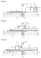
- Fig. 3 and Figs. 4A to 4C show the second embodiment, and the second embodiment will be described with reference to these accompanying drawings.
- Fig. 3 is a perspective view of the second embodiment, and Figs. 4A to 4C are sectional views along the center line of Fig. 3.
- Fig. 4A shows a state before a push rod is brought into contact with a semiconductor wafer
- Fig. 4B shows a state in which the push rod is in contact with the semiconductor wafer, and a probe is connected to a monitor circuit
- Fig. 4C shows a state in which the semiconductor wafer is being pushed upon contact between the push rod and the semiconductor wafer.
- a reinforcing plate 2 adhered to the semiconductor substrate (i.e., a wafer 1) described with reference to Figs. 4A to 4C is fitted in a recessed portion 31 provided in a plate fixing jig 3 shown in Fig. 3 such that an orientation flat 18 of the wafer 1 faces a pushing means.
- Another recessed portion 33 continues from the recessed portion 31 toward the pushing direction, so that loading/unloading of the reinforcing plate 2 can be facilitated.
- a heating unit (not shown) is arranged below the recessed portion 31 to heat an adhesive to about 130°C.
- a wafer push rod 41 is driven by a manipulator (not sown) controlled by a computer (not shown) and is moved along guide rails 44 formed on the table of the plate fixing jig 3.
- the wafer push rod 41 comprise an orientation flat (OF) pusher 45 which is brought into contact with the orientation flat 18 of the wafer 1 and a wafer pusher 46 which surrounds the OF pusher 45.
- a probe 5 comprising a probe tip 51, an arm 52, and a vertical moving mechanism 53 is mounted on the wafer push rod 41.
- An optical opening 34 is formed in the recessed portion 31 at a position immediately below the orientation flat 18.
- An LED 81 is arranged to face upward to cause light to pass through this opening 34.
- a photodiode 82 for detecting light from the LED 81 faces downward and is mounted on a sensor column 83.
- the reinforcing plate 2 comprises a light-transmitting substrate such as a quartz plate, and the wafer 1 does not transmit light therethrough.
- the photodiode 82 Before the wafer push rod 41 is brought into contact with the wafer 1, light emitted from the LED 81 and leaking from a gap between the wafer push rod 41 and the wafer 1 is detected by the photodiode 82 (Fig. 4A).
- the wafer push rod 41 which is moving toward the wafer 1 When the wafer push rod 41 which is moving toward the wafer 1 is brought into contact with the wafer 1, light from the gap is shielded, and the light-shielding state is detected by the photodiode 82.
- the probe tip 51 is moved downward by the vertical moving mechanism 53 and is contacted with the output terminals of the monitoring circuit which are provided on the back surface of the wafer 1 (Fig. 4B). This contacting operation may be performed during movement of the wafer push rod 41, or may be performed when movement is temporarily interrupted.
- the probe 5 keeps measuring the stresses generated in the wafer 1 and is kept moved together with the wafer push rod 41, i.e., the wafer 1 (Fig. 4
- the wafer 1 pushed and peeled from the reinforcing plate 2 is placed on rods 35 fixed to the table of the plate fixing jig 3.
- the arrangements of the monitor circuit and a control system are the same as those in the first embodiment.
- the wafer 1 is set in the plate fixing jig 3. At this time, the reinforcing plate 2 is accurately fitted into the recessed portion 31 of the jig 3.
- the operations of the peeling apparatus are controlled by a computer 63.
- the computer 63 stores a control program having a program for receiving a signal corresponding to a stress generated by the wafer 1 and processing this signal, and a program for controlling a speed for causing the wafer push rod 41 to push the wafer 1 by changing a speed of a motor 42 for driving a manipulator 43.
- this control program By executing this control program, the peeling operation is performed.
- the wafer 1 is pushed at an appropriate initial speed.
- the initial speed is about 10 ⁇ m/sec because care must be taken for initially pushing the wafer 1.
- electrical characteristics of the wafer 1 are measured to determine whether a stress exceeding a breakdown limit acts on the wafer 1. A relationship between the electrical characteristics and the stress exceeding the breakdown limit must be measured in a preliminary experiment in advance.
- the speed for pushing the wafer 1 is doubled, i.e., 20 ⁇ m/sec.
- the electrical characteristics of the wafer 1 are measured to determine whether the stress exceeding the breakdown limit acts on the wafer 1. If no stress exceeding the breakdown limit acts on the wafer 1, the speed for pushing he wafer 1 is doubled again, i.e., 40 ⁇ m/sec. The above operations are repeated unless the stress exceeding the breakdown limit acts on the wafer 1, thereby increasing the speed for pushing the wafer 1. If the stress exceeding the breakdown limit acts on the wafer 1 in the above repetition, the speed for pushing the wafer 1 is halved.
- the wafer 1 is pushed while the stress acting thereon is kept checked. Therefore, the wafer 1 can be peeled from the reinforcing plate 2 without damaging the wafer 1.
- the magnitude of the initial speed for pushing the wafer 1, a moving distance of the wafer 1 between measurements of electrical characteristics of the wafer 1, and degrees of acceleration and deceleration are not limited to the specific values described in the above embodiment. These may be appropriately determined in accordance with a size of the wafer 1, a type of adhesive, and other conditions.
- the stress generated in the wafer 1 is detected by the use of the monitoring circuit formed on the front surface of the wafer 1, but in stead of the detection of the stress generated in the wafer, on the basis of the detection of the load to be applied to the wafer, the pushing speed of the wafer push rod may be controlled.
- a load cell 54 for detecting the load applied to the wafer push rod is attached to the rod. The output of the load cell 54 is detected and the pushing speed of the load is controlled on the basis of the detected output.
Landscapes
- Testing Or Measuring Of Semiconductors Or The Like (AREA)
- Container, Conveyance, Adherence, Positioning, Of Wafer (AREA)
Applications Claiming Priority (2)
| Application Number | Priority Date | Filing Date | Title |
|---|---|---|---|
| JP96900/91 | 1991-04-26 | ||
| JP9690091 | 1991-04-26 |
Publications (3)
| Publication Number | Publication Date |
|---|---|
| EP0510706A2 true EP0510706A2 (fr) | 1992-10-28 |
| EP0510706A3 EP0510706A3 (en) | 1993-01-20 |
| EP0510706B1 EP0510706B1 (fr) | 1995-12-20 |
Family
ID=14177249
Family Applications (1)
| Application Number | Title | Priority Date | Filing Date |
|---|---|---|---|
| EP92107121A Expired - Lifetime EP0510706B1 (fr) | 1991-04-26 | 1992-04-26 | Dispositif pour retirer une couche protectrice d'un substrat semi-conducteur |
Country Status (4)
| Country | Link |
|---|---|
| US (1) | US5240546A (fr) |
| EP (1) | EP0510706B1 (fr) |
| CA (1) | CA2067027A1 (fr) |
| DE (1) | DE69206868T2 (fr) |
Cited By (2)
| Publication number | Priority date | Publication date | Assignee | Title |
|---|---|---|---|---|
| WO2003012873A1 (fr) * | 2001-07-31 | 2003-02-13 | Shin-Etsu Handotai Co., Ltd. | Procede de fabrication de plaquettes soi et gabarit de separation de plaquettes |
| US9138978B2 (en) | 2009-04-21 | 2015-09-22 | Ev Group Gmbh | Device for separating a substrate from a carrier substrate |
Families Citing this family (25)
| Publication number | Priority date | Publication date | Assignee | Title |
|---|---|---|---|---|
| US5432318A (en) * | 1992-05-15 | 1995-07-11 | Irvine Sensors Corporation | Apparatus for segmenting stacked IC chips |
| JP2642317B2 (ja) * | 1994-08-03 | 1997-08-20 | ソマール株式会社 | フィルム剥離方法及び装置 |
| DE69732157T2 (de) * | 1996-02-28 | 2005-12-29 | Ebara Corp. | Transportroboter mit Tropfwasserschutz |
| FR2752332B1 (fr) * | 1996-08-12 | 1998-09-11 | Commissariat Energie Atomique | Dispositif de decollement de plaquettes et procede de mise en oeuvre de ce dispositif |
| US6244931B1 (en) * | 1999-04-02 | 2001-06-12 | Applied Materials, Inc. | Buffer station on CMP system |
| DE19958803C1 (de) * | 1999-12-07 | 2001-08-30 | Fraunhofer Ges Forschung | Verfahren und Vorrichtung zum Handhaben von Halbleitersubstraten bei der Prozessierung und/oder Bearbeitung |
| US6309899B1 (en) * | 2000-02-22 | 2001-10-30 | Advanced Micro Devices, Inc. | Method and system for removing a die from a semiconductor package |
| US6415843B1 (en) * | 2001-01-10 | 2002-07-09 | Anadigics, Inc. | Spatula for separation of thinned wafer from mounting carrier |
| US6685795B1 (en) * | 2001-08-10 | 2004-02-03 | Adco Products, Inc. | Device and method of separating adhered layers |
| US7314076B2 (en) * | 2004-09-22 | 2008-01-01 | Northrup Grumman Corporation | Multilayer shim peeling device |
| US7314808B2 (en) * | 2004-12-23 | 2008-01-01 | Applied Materials, Inc. | Method for sequencing substrates |
| WO2006096165A2 (fr) * | 2005-03-04 | 2006-09-14 | Thomson Licensing | Appareil et procede permettant d'enlever un substrat provisoire d'un disque optique |
| JP2009154407A (ja) * | 2007-12-27 | 2009-07-16 | Tdk Corp | 剥離装置、剥離方法および情報記録媒体製造方法 |
| TW201015652A (en) * | 2008-10-07 | 2010-04-16 | Asia Ic Mic Process Inc | Separating device and method |
| US8251576B1 (en) | 2009-05-30 | 2012-08-28 | Mia Sole | Cold lift-off test for strength of film stack subjected to thermal loading |
| TWI534938B (zh) * | 2010-02-25 | 2016-05-21 | 尼康股份有限公司 | Substrate separation device, manufacturing method of semiconductor device, load lock device, substrate bonding device and substrate separation method |
| US8758552B2 (en) | 2010-06-07 | 2014-06-24 | Skyworks Solutions, Inc. | Debonders and related devices and methods for semiconductor fabrication |
| US8758553B2 (en) * | 2010-10-05 | 2014-06-24 | Skyworks Solutions, Inc. | Fixtures and methods for unbonding wafers by shear force |
| US8888085B2 (en) | 2010-10-05 | 2014-11-18 | Skyworks Solutions, Inc. | Devices and methodologies for handling wafers |
| US20120080832A1 (en) | 2010-10-05 | 2012-04-05 | Skyworks Solutions, Inc. | Devices for methodologies related to wafer carriers |
| CN103650171B (zh) * | 2011-07-15 | 2018-09-18 | 亮锐控股有限公司 | 将半导体装置结合到支持衬底的方法 |
| JP5913053B2 (ja) * | 2011-12-08 | 2016-04-27 | 東京エレクトロン株式会社 | 剥離装置、剥離システム、剥離方法、プログラム及びコンピュータ記憶媒体 |
| TWI571949B (zh) | 2013-01-10 | 2017-02-21 | 晶元光電股份有限公司 | 半導體元件翻轉裝置 |
| JP6128941B2 (ja) * | 2013-05-10 | 2017-05-17 | ルネサスエレクトロニクス株式会社 | 半導体装置の製造方法及び半導体製造装置 |
| JP7556320B2 (ja) * | 2021-04-15 | 2024-09-26 | 新光電気工業株式会社 | 基板取り外し装置 |
Family Cites Families (7)
| Publication number | Priority date | Publication date | Assignee | Title |
|---|---|---|---|---|
| US3634930A (en) * | 1969-06-12 | 1972-01-18 | Western Electric Co | Methods for bonding leads and testing bond strength |
| US4519168A (en) * | 1979-09-18 | 1985-05-28 | Speedfam Corporation | Liquid waxless fixturing of microsize wafers |
| US4433835A (en) * | 1981-11-30 | 1984-02-28 | Tencor Instruments | Wafer chuck with wafer cleaning feature |
| US4664739A (en) * | 1983-12-19 | 1987-05-12 | Stauffer Chemical Company | Removal of semiconductor wafers from dicing film |
| US4893513A (en) * | 1988-11-01 | 1990-01-16 | Nordson Corporation | Method and apparatus for bond testing |
| US5013392A (en) * | 1990-02-15 | 1991-05-07 | Hughes Aircraft Company | Thin film delamination tool |
| US5170929A (en) * | 1992-05-29 | 1992-12-15 | International Business Machines Corporation | Ultrasonic adhesion/dehesion monitoring apparatus with acoustic transducer means |
-
1992
- 1992-02-24 US US07/872,996 patent/US5240546A/en not_active Expired - Lifetime
- 1992-04-24 CA CA002067027A patent/CA2067027A1/fr not_active Abandoned
- 1992-04-26 DE DE69206868T patent/DE69206868T2/de not_active Expired - Fee Related
- 1992-04-26 EP EP92107121A patent/EP0510706B1/fr not_active Expired - Lifetime
Cited By (5)
| Publication number | Priority date | Publication date | Assignee | Title |
|---|---|---|---|---|
| WO2003012873A1 (fr) * | 2001-07-31 | 2003-02-13 | Shin-Etsu Handotai Co., Ltd. | Procede de fabrication de plaquettes soi et gabarit de separation de plaquettes |
| US6998329B2 (en) | 2001-07-31 | 2006-02-14 | Shin-Etsu Handotai Co., Ltd. | SOI wafer producing method, and wafer separating jig |
| EP1420452A4 (fr) * | 2001-07-31 | 2007-05-30 | Shinetsu Handotai Kk | Procede de fabrication de plaquettes soi et gabarit de separation de plaquettes |
| US9138978B2 (en) | 2009-04-21 | 2015-09-22 | Ev Group Gmbh | Device for separating a substrate from a carrier substrate |
| EP2422357B1 (fr) * | 2009-04-21 | 2020-07-01 | EV Group GmbH | Procédé et dispositif utilisés pour séparer un substrat d'un substrat support |
Also Published As
| Publication number | Publication date |
|---|---|
| US5240546A (en) | 1993-08-31 |
| DE69206868T2 (de) | 1996-08-14 |
| EP0510706B1 (fr) | 1995-12-20 |
| EP0510706A3 (en) | 1993-01-20 |
| CA2067027A1 (fr) | 1992-10-27 |
| DE69206868D1 (de) | 1996-02-01 |
Similar Documents
| Publication | Publication Date | Title |
|---|---|---|
| EP0510706B1 (fr) | Dispositif pour retirer une couche protectrice d'un substrat semi-conducteur | |
| US6162701A (en) | Semiconductor device and method for making same | |
| US5525549A (en) | Method for producing an acceleration sensor | |
| US6608370B1 (en) | Semiconductor wafer having a thin die and tethers and methods of making the same | |
| US6472240B2 (en) | Methods of semiconductor processing | |
| KR930002811B1 (ko) | 동시 접합 작업에 적합한 집적회로 리드 프레임 | |
| EP0259816B1 (fr) | Méthode et dispositif de fixation d'un élément laser à semi-conducteur | |
| EP0558795B1 (fr) | Procédé pour la fabrication de puces à semiconducteur | |
| EP4227979A1 (fr) | Système de collage et procédé de collage | |
| KR20100017103A (ko) | 싱귤레이팅된 다이의 테스트를 위한 방법 및 장치 | |
| KR20030095351A (ko) | 미소 반도체 소자의 제조 방법 | |
| US20020067982A1 (en) | Pickup apparatus for semiconductor chips | |
| US3998377A (en) | Method of and apparatus for bonding workpieces | |
| EP1336986B1 (fr) | Procédé de séparation d'une puce semicondutrice mince d'une plaquette | |
| CN113436988B (zh) | 芯片贴装装置、剥离夹具以及半导体器件的制造方法 | |
| KR20010021167A (ko) | 콘택터용 픽킹 및 배치 기구 | |
| JP3191827B2 (ja) | 半導体基板の剥離装置 | |
| US12300482B2 (en) | Element chip manufacturing method and substrate processing method | |
| JPH06151946A (ja) | 半導体受光素子およびその製造方法 | |
| JPH11345785A (ja) | ダイシング方法およびダイシング装置 | |
| JPH0732281B2 (ja) | 劈開装置及び劈開方法 | |
| EP0306890A1 (fr) | Module semi-conducteur comprenant des dispositifs actifs disposés dans des cavités d'un substrat | |
| KR930010075B1 (ko) | 집적 회로용 리드프레임 및 소켓 | |
| CN119521900A (zh) | 一种发光模组制作方法、发光模组和发光装置 | |
| JPH08248042A (ja) | プローブ顕微鏡用探触子の製造方法 |
Legal Events
| Date | Code | Title | Description |
|---|---|---|---|
| PUAI | Public reference made under article 153(3) epc to a published international application that has entered the european phase |
Free format text: ORIGINAL CODE: 0009012 |
|
| AK | Designated contracting states |
Kind code of ref document: A2 Designated state(s): DE FR GB NL SE |
|
| PUAL | Search report despatched |
Free format text: ORIGINAL CODE: 0009013 |
|
| AK | Designated contracting states |
Kind code of ref document: A3 Designated state(s): DE FR GB NL SE |
|
| 17P | Request for examination filed |
Effective date: 19930720 |
|
| 17Q | First examination report despatched |
Effective date: 19940609 |
|
| GRAA | (expected) grant |
Free format text: ORIGINAL CODE: 0009210 |
|
| AK | Designated contracting states |
Kind code of ref document: B1 Designated state(s): DE FR GB NL SE |
|
| PG25 | Lapsed in a contracting state [announced via postgrant information from national office to epo] |
Ref country code: NL Free format text: LAPSE BECAUSE OF FAILURE TO SUBMIT A TRANSLATION OF THE DESCRIPTION OR TO PAY THE FEE WITHIN THE PRESCRIBED TIME-LIMIT Effective date: 19951220 Ref country code: FR Effective date: 19951220 |
|
| REF | Corresponds to: |
Ref document number: 69206868 Country of ref document: DE Date of ref document: 19960201 |
|
| PG25 | Lapsed in a contracting state [announced via postgrant information from national office to epo] |
Ref country code: SE Effective date: 19960320 |
|
| PGFP | Annual fee paid to national office [announced via postgrant information from national office to epo] |
Ref country code: DE Payment date: 19960429 Year of fee payment: 5 |
|
| EN | Fr: translation not filed | ||
| PGFP | Annual fee paid to national office [announced via postgrant information from national office to epo] |
Ref country code: GB Payment date: 19960529 Year of fee payment: 5 |
|
| NLV1 | Nl: lapsed or annulled due to failure to fulfill the requirements of art. 29p and 29m of the patents act | ||
| PLBE | No opposition filed within time limit |
Free format text: ORIGINAL CODE: 0009261 |
|
| STAA | Information on the status of an ep patent application or granted ep patent |
Free format text: STATUS: NO OPPOSITION FILED WITHIN TIME LIMIT |
|
| 26N | No opposition filed | ||
| PG25 | Lapsed in a contracting state [announced via postgrant information from national office to epo] |
Ref country code: GB Effective date: 19970426 |
|
| GBPC | Gb: european patent ceased through non-payment of renewal fee |
Effective date: 19970426 |
|
| PG25 | Lapsed in a contracting state [announced via postgrant information from national office to epo] |
Ref country code: DE Free format text: LAPSE BECAUSE OF NON-PAYMENT OF DUE FEES Effective date: 19980101 |