EP0512607A2 - Verfahren zur Herstellung eines Halbleiterbauelements mit Ionenimplantierung - Google Patents
Verfahren zur Herstellung eines Halbleiterbauelements mit Ionenimplantierung Download PDFInfo
- Publication number
- EP0512607A2 EP0512607A2 EP92201160A EP92201160A EP0512607A2 EP 0512607 A2 EP0512607 A2 EP 0512607A2 EP 92201160 A EP92201160 A EP 92201160A EP 92201160 A EP92201160 A EP 92201160A EP 0512607 A2 EP0512607 A2 EP 0512607A2
- Authority
- EP
- European Patent Office
- Prior art keywords
- groove
- grooves
- photoresist
- photoresist layer
- irradiation
- Prior art date
- Legal status (The legal status is an assumption and is not a legal conclusion. Google has not performed a legal analysis and makes no representation as to the accuracy of the status listed.)
- Granted
Links
Images

Classifications
-
- H—ELECTRICITY
- H10—SEMICONDUCTOR DEVICES; ELECTRIC SOLID-STATE DEVICES NOT OTHERWISE PROVIDED FOR
- H10D—INORGANIC ELECTRIC SEMICONDUCTOR DEVICES
- H10D44/00—Charge transfer devices
- H10D44/01—Manufacture or treatment
- H10D44/041—Manufacture or treatment having insulated gates
-
- H—ELECTRICITY
- H10—SEMICONDUCTOR DEVICES; ELECTRIC SOLID-STATE DEVICES NOT OTHERWISE PROVIDED FOR
- H10D—INORGANIC ELECTRIC SEMICONDUCTOR DEVICES
- H10D48/00—Individual devices not covered by groups H10D1/00 - H10D44/00
- H10D48/30—Devices controlled by electric currents or voltages
- H10D48/32—Devices controlled by only the electric current supplied, or only the electric potential applied, to an electrode which does not carry the current to be rectified, amplified or switched
- H10D48/36—Unipolar devices
-
- H—ELECTRICITY
- H10—SEMICONDUCTOR DEVICES; ELECTRIC SOLID-STATE DEVICES NOT OTHERWISE PROVIDED FOR
- H10P—GENERIC PROCESSES OR APPARATUS FOR THE MANUFACTURE OR TREATMENT OF DEVICES COVERED BY CLASS H10
- H10P30/00—Ion implantation into wafers, substrates or parts of devices
- H10P30/20—Ion implantation into wafers, substrates or parts of devices into semiconductor materials, e.g. for doping
- H10P30/22—Ion implantation into wafers, substrates or parts of devices into semiconductor materials, e.g. for doping using masks
-
- H—ELECTRICITY
- H10—SEMICONDUCTOR DEVICES; ELECTRIC SOLID-STATE DEVICES NOT OTHERWISE PROVIDED FOR
- H10P—GENERIC PROCESSES OR APPARATUS FOR THE MANUFACTURE OR TREATMENT OF DEVICES COVERED BY CLASS H10
- H10P30/00—Ion implantation into wafers, substrates or parts of devices
- H10P30/20—Ion implantation into wafers, substrates or parts of devices into semiconductor materials, e.g. for doping
- H10P30/222—Ion implantation into wafers, substrates or parts of devices into semiconductor materials, e.g. for doping characterised by the angle between the ion beam and the crystal planes or the main crystal surface
-
- H—ELECTRICITY
- H10—SEMICONDUCTOR DEVICES; ELECTRIC SOLID-STATE DEVICES NOT OTHERWISE PROVIDED FOR
- H10P—GENERIC PROCESSES OR APPARATUS FOR THE MANUFACTURE OR TREATMENT OF DEVICES COVERED BY CLASS H10
- H10P76/00—Manufacture or treatment of masks on semiconductor bodies, e.g. by lithography or photolithography
- H10P76/20—Manufacture or treatment of masks on semiconductor bodies, e.g. by lithography or photolithography of masks comprising organic materials
- H10P76/204—Manufacture or treatment of masks on semiconductor bodies, e.g. by lithography or photolithography of masks comprising organic materials of organic photoresist masks
- H10P76/2041—Photolithographic processes
-
- H—ELECTRICITY
- H10—SEMICONDUCTOR DEVICES; ELECTRIC SOLID-STATE DEVICES NOT OTHERWISE PROVIDED FOR
- H10W—GENERIC PACKAGES, INTERCONNECTIONS, CONNECTORS OR OTHER CONSTRUCTIONAL DETAILS OF DEVICES COVERED BY CLASS H10
- H10W10/00—Isolation regions in semiconductor bodies between components of integrated devices
- H10W10/01—Manufacture or treatment
- H10W10/011—Manufacture or treatment of isolation regions comprising dielectric materials
- H10W10/014—Manufacture or treatment of isolation regions comprising dielectric materials using trench refilling with dielectric materials, e.g. shallow trench isolations
- H10W10/0148—Manufacture or treatment of isolation regions comprising dielectric materials using trench refilling with dielectric materials, e.g. shallow trench isolations comprising introducing impurities in side walls or bottom walls of trenches, e.g. for forming channel stoppers
-
- H—ELECTRICITY
- H10—SEMICONDUCTOR DEVICES; ELECTRIC SOLID-STATE DEVICES NOT OTHERWISE PROVIDED FOR
- H10W—GENERIC PACKAGES, INTERCONNECTIONS, CONNECTORS OR OTHER CONSTRUCTIONAL DETAILS OF DEVICES COVERED BY CLASS H10
- H10W10/00—Isolation regions in semiconductor bodies between components of integrated devices
- H10W10/10—Isolation regions comprising dielectric materials
- H10W10/17—Isolation regions comprising dielectric materials formed using trench refilling with dielectric materials, e.g. shallow trench isolations
-
- Y—GENERAL TAGGING OF NEW TECHNOLOGICAL DEVELOPMENTS; GENERAL TAGGING OF CROSS-SECTIONAL TECHNOLOGIES SPANNING OVER SEVERAL SECTIONS OF THE IPC; TECHNICAL SUBJECTS COVERED BY FORMER USPC CROSS-REFERENCE ART COLLECTIONS [XRACs] AND DIGESTS
- Y10—TECHNICAL SUBJECTS COVERED BY FORMER USPC
- Y10S—TECHNICAL SUBJECTS COVERED BY FORMER USPC CROSS-REFERENCE ART COLLECTIONS [XRACs] AND DIGESTS
- Y10S438/00—Semiconductor device manufacturing: process
- Y10S438/942—Masking
- Y10S438/948—Radiation resist
- Y10S438/949—Energy beam treating radiation resist on semiconductor
Definitions
- the invention relates to a method of manufacturing a semiconductor device whereby a semiconductor body is provided at a surface with at least one groove which extends from the surface into the semiconductor body, a zone doped with an impurity being provided in a portion of the groove by means of ion implantation through a mask.
- the invention also relates to a semiconductor device manufactured by such a method.
- the groove which may have, for example, a U- or V-shape, may form a separation region between active regions, such as an island insulation in bipolar circuits.
- a conducting layer is provided in the groove, forming a gate electrode of a charge-coupled device such as described in, for example, the European Patent Application EP 0 239 151 filed by Applicant and laid open to public inspection on 30.09.87.
- the transport channel is situated in a mesa limited by two parallel grooves, the charge transport taking place along the walls of the mesa. Zones are formed locally in the walls, defining the charge storage locations in the channel.
- US Patent 4,446,178 describes a method by which groove walls are doped by oblique implantation. In this method, doped zones are provided over the entire length of the grooves. It is often desirable, however, to provide the walls and/or the bottom of the groove or grooves only locally with doped zones which are provided over only a portion of the groove length.
- a method of the kind described in the opening paragraph is known from US Patent 4,756,793.
- the grooves are temporarily filled up with a filler material, for example photoresist, so that an at least substantially plane surface is obtained.
- a filler material for example photoresist
- an implantation mask of metal for example Al
- the filler material is then removed from the groove or grooves at least at the areas of the windows in the implantation mask, or from the entire groove or grooves, upon which the implantation is carried out through the windows in the implantation mask.
- the implantation mask is then removed again.
- the invention has for its object inter alia to provide a method which comprises considerably fewer steps than does the known method, and is thus much simpler, while a high mask definition is retained.
- a method of the kind described in the opening paragraph, according to the invention is characterized in that a positive photoresist layer is provided on the surface and in the groove, in that the photoresist layer is masked against irradiation at the area of the ion implantation to be carried out and the non-masked portions of the photoresist layer are subjected to irradiation, after which the irradiated portions of the photoresist layer are rendered insoluble by means of an image reversal process, and in that subsequently the photoresist layer is subjected to irradiation in a second irradiation step at the area of the ion implantation to be carried out, after which the portions of the photoresist layer masked during the irradiation step first mentioned are removed by development.
- an implantation mask may be obtained in this way which has a sharp definition at the surface and at the same time leaves the groove exposed over its entire thickness wherever implantation is to take place.
- the first irradiation step may be carried out with a comparatively low irradiation dose, so that a sharp mask definition at the surface is achieved.
- a possible result of this comparatively low dose is that the photoresist is not fully irradiated down to the bottom, so that the windows in the implantation mask to be formed become greater in the depth direction of the groove. This is not a disadvantage, however, because of the shadow effect of the implantation mask.
- the second irradiation step which only serves to render the remaining portions of the photoresist layer soluble, may be carried out with a comparatively high dose in such a way that the photoresist is irradiated throughout its entire thickness. It is ensured in this way that the photoresist is removed throughout the entire depth of the groove (or grooves) at the areas of the windows in the implantation mask.
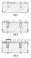
- Figs. 1-7 show in a purely diagrammatical way how by means of a method according to the invention one or several doped zones can be implanted in very narrow and comparatively deep grooves over only a portion of the length in the walls and/or the bottom of the groove or grooves.
- Fig. 5 for this purpose shows a portion of the device in perspective view;
- Figs. 2-4 and 6 show the device in a cross-section corresponding to the front face in Fig. 5;
- Fig. 7b gives a cross-section in the longitudinal direction of the groove; and
- Fig. 7a gives the same section when a conventional method is used.
- the starting material is, for example, a semiconductor substrate 1 of silicon (see Fig. 1). Grooves, of which only two are shown in Fig. 3, are etched into the surface 2. These grooves, which have, for example, a width of approximately 1 micron and a depth of approximately 4 microns, and which are therefore very narrow in relation to their depth, may be formed by a method known per se , for example, by reactive ion etching (RIE). Such grooves may be formed for various purposes and are often used as separation grooves between the portions of a monolithic integrated circuit.
- the grooves 3 are etched by means of an oxide mask 4 on the surface 2 outside the region of the grooves.
- the oxide layer 4 has a thickness of 0.5 micron.
- An approximately 20 nm thick oxide layer 5 is grown on the walls and the bottom of the grooves 3 by means of a light thermal oxidation.
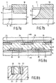
- a positive photoresist layer 6 is then provided on the surface 2 and in the grooves 3 for the implantation mask.
- “Positive” here denotes a photoresist of which the illuminated portions are removed during normal use after illumination and development.
- the photoresist marketed by the Hunt Company under the name HPR 204 is used for the layer 6.
- the thickness of the layer 6 outside the grooves is approximately 1,3 microns (see Fig. 3).
- the photoresist layer 6 is irradiated or illuminated, indicated in Fig. 3 with the arrows 8, through a mask 7 which masks the photoresist 6 at the areas of openings in the implantation mask to be formed.
- the illumination intensity is chosen to be comparatively low, i.e. the photoresist layer 6 is effectively illuminated in the grooves not throughout the entire thickness, down to the bottom of the grooves, but only to approximately halfway the groove, i.e. to a depth of 1 to 2 microns. This comparatively weak intensity renders a sharp definition of the implantation mask possible.
- an image reversal step is carried out by which the illuminated portion of the photoresist 6 becomes insoluble during the development of the photoresist at a later stage.
- image reversal steps are known per se , for example, from the article "Image Reversal, Applications for Micron and Sub-Micron Patterning" by S.K. Jones et al., published in Proc. Electr. Soc. 1987, pp. 190-210.
- Acid is formed in the photoresist owing to the illumination.
- a gas flow containing NH3 is conducted over the device, for example, during 30 minutes at a temperature of 105° C, so that the illuminated, acid region in the photoresist becomes insoluble (in the developer).
- a maskless illumination step is carried out, indicated diagrammatically by the arrows 9 in the drawing.
- the intensity of the illumination 9 is so chosen that, at a given illumination time, the photoresist layer 6 is illuminated throughout its entire thickness, also in the grooves 3.
- the portions of the photoresist layer 6 masked during the first illumination step are rendered insoluble for the ensuing development step by this.
- the photoresist layer 6 is developed in, for example, a 1 : 1 solution of a developer marketed under the name LSI by the Waycoat Company.
- the development time is so chosen that the photoresist 6, at least the portion illuminated during the step shown in Fig. 4, is removed over its entire thickness, down to the bottom of the grooves. Since the photoresist has been rendered insoluble in the grooves only to approximately halfway down the groove depth during the image reversal step, owing to the preceding weak illumination, the photoresist is also removed by the developer in the grooves below the implantation mask obtained (see Fig. 5). Since the masking is based on a shadow effect, this is not a disadvantage.
- the impurity is implanted in the grooves 3, which is diagrammatically shown by the arrows 12.
- the impurity may be, for example, an n- or p-type dopant.
- the angle ⁇ is so chosen that the side walls of the grooves 3 are provided with a doped zone 13.
- the depth of the zone 13 may also be adjusted by means of the implantation angle. If the opposite wall is to be doped, the semiconductor body may be rotated through an angle of 180°.
- Other zones may be provided, for example, having a different conductivity type or the same conductivity type but a different concentration in that the process described above is repeated.
- the implantation mask 10 may be removed after the implantation, upon which the device is subjected to further necessary process steps which are outside the scope of the invention and are accordingly not described here any further.
- Fig. 7a shows a longitudinal section of a groove in a portion of the device comprising the edge of a window 11.
- the mask 10 does not have a straight wall 14 perpendicular to the surface 2, but a wall with a slope, so that the window 11 in the implantation mask 10 becomes wider from top to bottom.
- the portion of the groove wall which is doped is determined, as a result of the shadow effect, by the portion of the mask situated on the surface 2.
- the boundary between the implanted and the non-implanted portion of the groove is indicated with the broken line 15 in Fig. 7a.
- Fig. 7b shows the same section as Fig. 7a with a photoresist mask 10 manufactured in a conventional manner.
- the photoresist mask 10 is again formed from a positive photoresist of which the portions to be removed are defined in usual manner by a single illumination and removed through development. Owing to the comparatively great thickness of the photoresist in the groove 3 and the decreasing illumination intensity in the depth direction of the groove, the photoresist mask 10 is given the profile 14 shown in Fig. 7b, the window 11 becoming smaller in vertical direction. Accordingly, the window 11 is smaller in the groove than at the surface, so that the region in the groove to be implanted is no longer well-defined.
- the photoresist profile 14 of Fig. 7a could in principle also be obtained through the use of a negative photoresist and a single illumination.
- positive photoresists are preferred in semiconductor technology, one of the reasons being that it is more difficult to make very small windows in negative photoresists, which imposes limitations on the smallest possible dimensions in the device to be manufactured.
- Figs. 8a and 8b show a charge-coupled device manufactured by the method described above in plan view and in cross-section taken on the line b-b, respectively.
- the device comprises a mesa-shaped channel 21 which is bounded in its longitudinal direction by two grooves 22. The walls and the bottom of the grooves are covered with a thin oxide layer 5.
- the grooves are further filled with tracks 23 of a conducting material, for example polycrystalline silicon, which form the gate electrodes of the charge-coupled device. During operation, the charge is transported in zigzag manner through the channel, in Fig.
- the sides of the mesa i.e. the walls of the grooves 22, are for that purpose provided with doped zones 24 and 25 which form transfer regions and storage regions, respectively.
- the zones 24, 25 may be of the same conductivity type, for example the n-type, assuming that the device is of the n-channel type, the zones 25 having a higher concentration than the zones 24.
- the zones 24, 25 may be formed by ion implantation, the more weakly doped zones 24 being provided first, for example, by means of a photomask formed by the method described above.
- these zones are so provided that they overlap the regions of the zones 25 to be provided later. Then a new implantation mask of photoresist is provided which leaves the areas of the zones 25 exposed, upon which the zones 25 are formed by a second implantation.
- the grooves may form insulating regions between adjoining active regions, various circuit elements of the circuit being provided in the grooves, as described in the US Patent 4,446,178 cited above.
- Photoresists other than those mentioned here may alternatively be used for the method described, as well as photoresists which are irradiated with electrons instead of with light (visible or UV). It is possible to illuminate down to the bottom of the groove by electron beam illumination of positive photoresist.
- An implantation mask 10 (see Figs. 5 and 6) may be obtained in this way which extends down to the bottom of the groove 3.
Landscapes
- Element Separation (AREA)
- Exposure And Positioning Against Photoresist Photosensitive Materials (AREA)
- Solid State Image Pick-Up Elements (AREA)
- Drying Of Semiconductors (AREA)
Applications Claiming Priority (2)
| Application Number | Priority Date | Filing Date | Title |
|---|---|---|---|
| EP91201052 | 1991-05-03 | ||
| EP91201052 | 1991-05-03 |
Publications (3)
| Publication Number | Publication Date |
|---|---|
| EP0512607A2 true EP0512607A2 (de) | 1992-11-11 |
| EP0512607A3 EP0512607A3 (en) | 1993-09-08 |
| EP0512607B1 EP0512607B1 (de) | 1997-07-16 |
Family
ID=8207635
Family Applications (1)
| Application Number | Title | Priority Date | Filing Date |
|---|---|---|---|
| EP92201160A Expired - Lifetime EP0512607B1 (de) | 1991-05-03 | 1992-04-24 | Verfahren zur Herstellung eines Halbleiterbauelements mit Ionenimplantierung |
Country Status (7)
| Country | Link |
|---|---|
| US (1) | US5306390A (de) |
| EP (1) | EP0512607B1 (de) |
| JP (1) | JP3242446B2 (de) |
| KR (1) | KR100256454B1 (de) |
| CN (1) | CN1029273C (de) |
| DE (1) | DE69220846T2 (de) |
| PL (1) | PL168460B1 (de) |
Cited By (2)
| Publication number | Priority date | Publication date | Assignee | Title |
|---|---|---|---|---|
| EP1701686A4 (de) * | 2003-12-19 | 2009-07-01 | Third Dimension 3D Sc Inc | Verfahren zur herstellung einer superverbindungsvorrichtung mit herkömmlichen enden |
| EP1706900A4 (de) * | 2003-12-19 | 2009-07-22 | Third Dimension 3D Sc Inc | Verfahren zur herstellung eines superjunction-bauelements mit breiten mesas |
Families Citing this family (13)
| Publication number | Priority date | Publication date | Assignee | Title |
|---|---|---|---|---|
| JP2611728B2 (ja) * | 1993-11-02 | 1997-05-21 | 日本電気株式会社 | 動画像符号化復号化方式 |
| KR100335546B1 (ko) * | 1994-04-15 | 2002-10-11 | 코닌클리케 필립스 일렉트로닉스 엔.브이. | 지지바에 기초한 반도체 디바이스 제조 방법 |
| US5668018A (en) * | 1995-06-07 | 1997-09-16 | International Business Machines Corporation | Method for defining a region on a wall of a semiconductor structure |
| US6440638B2 (en) | 1998-09-28 | 2002-08-27 | International Business Machines Corp. | Method and apparatus for resist planarization |
| US6100172A (en) * | 1998-10-29 | 2000-08-08 | International Business Machines Corporation | Method for forming a horizontal surface spacer and devices formed thereby |
| US6096598A (en) * | 1998-10-29 | 2000-08-01 | International Business Machines Corporation | Method for forming pillar memory cells and device formed thereby |
| US6194268B1 (en) | 1998-10-30 | 2001-02-27 | International Business Machines Corporation | Printing sublithographic images using a shadow mandrel and off-axis exposure |
| US6150256A (en) * | 1998-10-30 | 2000-11-21 | International Business Machines Corporation | Method for forming self-aligned features |
| TW523860B (en) * | 2002-03-22 | 2003-03-11 | Nanya Technology Corp | Manufacturing method for lower electrode plate of capacitors in memory |
| US6780736B1 (en) * | 2003-06-20 | 2004-08-24 | International Business Machines Corporation | Method for image reversal of implant resist using a single photolithography exposure and structures formed thereby |
| KR101983672B1 (ko) | 2012-11-07 | 2019-05-30 | 삼성전자 주식회사 | 반도체 장치의 제조 방법 |
| CN103896204A (zh) * | 2012-12-25 | 2014-07-02 | 上海华虹宏力半导体制造有限公司 | 沟槽中的成膜工艺方法 |
| US10854455B2 (en) * | 2016-11-21 | 2020-12-01 | Marvell Asia Pte, Ltd. | Methods and apparatus for fabricating IC chips with tilted patterning |
Family Cites Families (6)
| Publication number | Priority date | Publication date | Assignee | Title |
|---|---|---|---|---|
| US4466178A (en) * | 1981-06-25 | 1984-08-21 | Rockwell International Corporation | Method of making extremely small area PNP lateral transistor by angled implant of deep trenches followed by refilling the same with dielectrics |
| US4466180A (en) * | 1981-06-25 | 1984-08-21 | Rockwell International Corporation | Method of manufacturing punch through voltage regulator diodes utilizing shaping and selective doping |
| EP0069191A1 (de) * | 1981-06-25 | 1983-01-12 | Rockwell International Corporation | Komplementäre NPN- und PNP- Lateraltransistoren, die zur minimalen Beeinflussung durch mit Substratoxyd gefüllte, sich kreuzende Rillen vom Substrat getrennt sind, und Verfahren zu ihrer Herstellung |
| NL8502765A (nl) * | 1985-10-10 | 1987-05-04 | Philips Nv | Werkwijze ter vervaardiging van een halfgeleiderinrichting. |
| NL8600786A (nl) * | 1986-03-27 | 1987-10-16 | Philips Nv | Ladingsgekoppelde inrichting. |
| US4693781A (en) * | 1986-06-26 | 1987-09-15 | Motorola, Inc. | Trench formation process |
-
1992
- 1992-04-24 EP EP92201160A patent/EP0512607B1/de not_active Expired - Lifetime
- 1992-04-24 DE DE69220846T patent/DE69220846T2/de not_active Expired - Fee Related
- 1992-04-28 JP JP13577792A patent/JP3242446B2/ja not_active Expired - Fee Related
- 1992-04-30 US US07/876,952 patent/US5306390A/en not_active Expired - Fee Related
- 1992-04-30 KR KR1019920007368A patent/KR100256454B1/ko not_active Expired - Fee Related
- 1992-04-30 CN CN92103136A patent/CN1029273C/zh not_active Expired - Fee Related
- 1992-04-30 PL PL92294400A patent/PL168460B1/pl unknown
Cited By (3)
| Publication number | Priority date | Publication date | Assignee | Title |
|---|---|---|---|---|
| EP1701686A4 (de) * | 2003-12-19 | 2009-07-01 | Third Dimension 3D Sc Inc | Verfahren zur herstellung einer superverbindungsvorrichtung mit herkömmlichen enden |
| EP1706900A4 (de) * | 2003-12-19 | 2009-07-22 | Third Dimension 3D Sc Inc | Verfahren zur herstellung eines superjunction-bauelements mit breiten mesas |
| US7704864B2 (en) | 2003-12-19 | 2010-04-27 | Third Dimension (3D) Semiconductor, Inc. | Method of manufacturing a superjunction device with conventional terminations |
Also Published As
| Publication number | Publication date |
|---|---|
| DE69220846D1 (de) | 1997-08-21 |
| CN1029273C (zh) | 1995-07-05 |
| PL168460B1 (pl) | 1996-02-29 |
| KR100256454B1 (ko) | 2000-05-15 |
| KR920022559A (ko) | 1992-12-19 |
| US5306390A (en) | 1994-04-26 |
| JP3242446B2 (ja) | 2001-12-25 |
| PL294400A1 (en) | 1992-11-16 |
| EP0512607A3 (en) | 1993-09-08 |
| DE69220846T2 (de) | 1998-02-12 |
| JPH0620983A (ja) | 1994-01-28 |
| EP0512607B1 (de) | 1997-07-16 |
| CN1066530A (zh) | 1992-11-25 |
Similar Documents
| Publication | Publication Date | Title |
|---|---|---|
| US5789300A (en) | Method of making IGFETs in densely and sparsely populated areas of a substrate | |
| EP0512607B1 (de) | Verfahren zur Herstellung eines Halbleiterbauelements mit Ionenimplantierung | |
| US4232439A (en) | Masking technique usable in manufacturing semiconductor devices | |
| US4763183A (en) | Semiconductor-on-insulator (SOI) devices and SOI IC fabrication method | |
| US5448094A (en) | Concave channel MOS transistor and method of fabricating the same | |
| US4394182A (en) | Microelectronic shadow masking process for reducing punchthrough | |
| US4160987A (en) | Field effect transistors with polycrystalline silicon gate self-aligned to both conductive and non-conductive regions and fabrication of integrated circuits containing the transistors | |
| US4393572A (en) | Method of making low leakage N-channel SOS transistors utilizing positive photoresist masking techniques | |
| JPH0358173B2 (de) | ||
| EP0090447B1 (de) | Maskierungsverfahren zum Herstellen einer Halbleiteranordnung | |
| EP0191037B1 (de) | Halbleiter auf isolator-(soi)-anordnungen und verfahren zur herstellung von soi integrierten schaltungen | |
| JPH0666466B2 (ja) | 半導体装置の製造方法 | |
| GB2111305A (en) | Method of forming ion implanted regions self-aligned with overlying insulating layer portions | |
| EP0072660B1 (de) | Feldeffekttransistor und Verfahren zu dessen Herstellung | |
| JPH10256394A (ja) | 半導体構造体およびデバイス | |
| US6200887B1 (en) | Method to form a smooth gate polysilicon sidewall in the fabrication of integrated circuits | |
| US4268952A (en) | Method for fabricating self-aligned high resolution non planar devices employing low resolution registration | |
| US5523605A (en) | Semiconductor device and method for forming the same | |
| KR100252899B1 (ko) | 마스크 롬 및 그 제조방법 | |
| KR100242378B1 (ko) | 전계효과 트랜지스터의 게이트 제조방법 | |
| KR100371284B1 (ko) | 플랫 셀형 반도체 메모리 장치의 제조 방법 | |
| KR100324325B1 (ko) | 정전방전방지용 모스 트랜지스터 제조방법 | |
| KR19990050862A (ko) | 반도체소자 및 이의 제조방법 | |
| KR0144169B1 (ko) | 반도체 소자의 콘택형성방법 | |
| CA1200617A (en) | Microelectronic shadow masking process for reducing punchthrough |
Legal Events
| Date | Code | Title | Description |
|---|---|---|---|
| PUAI | Public reference made under article 153(3) epc to a published international application that has entered the european phase |
Free format text: ORIGINAL CODE: 0009012 |
|
| AK | Designated contracting states |
Kind code of ref document: A2 Designated state(s): DE FR GB IT |
|
| PUAL | Search report despatched |
Free format text: ORIGINAL CODE: 0009013 |
|
| AK | Designated contracting states |
Kind code of ref document: A3 Designated state(s): DE FR GB IT |
|
| 17P | Request for examination filed |
Effective date: 19940228 |
|
| 17Q | First examination report despatched |
Effective date: 19950530 |
|
| GRAG | Despatch of communication of intention to grant |
Free format text: ORIGINAL CODE: EPIDOS AGRA |
|
| GRAH | Despatch of communication of intention to grant a patent |
Free format text: ORIGINAL CODE: EPIDOS IGRA |
|
| GRAH | Despatch of communication of intention to grant a patent |
Free format text: ORIGINAL CODE: EPIDOS IGRA |
|
| GRAA | (expected) grant |
Free format text: ORIGINAL CODE: 0009210 |
|
| AK | Designated contracting states |
Kind code of ref document: B1 Designated state(s): DE FR GB IT |
|
| REF | Corresponds to: |
Ref document number: 69220846 Country of ref document: DE Date of ref document: 19970821 |
|
| ITF | It: translation for a ep patent filed | ||
| ET | Fr: translation filed | ||
| PLBE | No opposition filed within time limit |
Free format text: ORIGINAL CODE: 0009261 |
|
| STAA | Information on the status of an ep patent application or granted ep patent |
Free format text: STATUS: NO OPPOSITION FILED WITHIN TIME LIMIT |
|
| 26N | No opposition filed | ||
| REG | Reference to a national code |
Ref country code: FR Ref legal event code: CD |
|
| PGFP | Annual fee paid to national office [announced via postgrant information from national office to epo] |
Ref country code: FR Payment date: 20010423 Year of fee payment: 10 |
|
| PGFP | Annual fee paid to national office [announced via postgrant information from national office to epo] |
Ref country code: GB Payment date: 20010430 Year of fee payment: 10 |
|
| PGFP | Annual fee paid to national office [announced via postgrant information from national office to epo] |
Ref country code: DE Payment date: 20010620 Year of fee payment: 10 |
|
| REG | Reference to a national code |
Ref country code: GB Ref legal event code: IF02 |
|
| PG25 | Lapsed in a contracting state [announced via postgrant information from national office to epo] |
Ref country code: GB Free format text: LAPSE BECAUSE OF NON-PAYMENT OF DUE FEES Effective date: 20020424 |
|
| PG25 | Lapsed in a contracting state [announced via postgrant information from national office to epo] |
Ref country code: DE Free format text: LAPSE BECAUSE OF NON-PAYMENT OF DUE FEES Effective date: 20021101 |
|
| GBPC | Gb: european patent ceased through non-payment of renewal fee |
Effective date: 20020424 |
|
| PG25 | Lapsed in a contracting state [announced via postgrant information from national office to epo] |
Ref country code: FR Free format text: LAPSE BECAUSE OF NON-PAYMENT OF DUE FEES Effective date: 20021231 |
|
| REG | Reference to a national code |
Ref country code: FR Ref legal event code: ST |
|
| PG25 | Lapsed in a contracting state [announced via postgrant information from national office to epo] |
Ref country code: IT Free format text: LAPSE BECAUSE OF NON-PAYMENT OF DUE FEES;WARNING: LAPSES OF ITALIAN PATENTS WITH EFFECTIVE DATE BEFORE 2007 MAY HAVE OCCURRED AT ANY TIME BEFORE 2007. THE CORRECT EFFECTIVE DATE MAY BE DIFFERENT FROM THE ONE RECORDED. Effective date: 20050424 |