EP0514547A1 - MEMOIRE A SEMI-CONDUCTEUR UTILISANT UN CONDENSATEUR FERROELECTRIQUE ET UNE COUCHE DE PROTECTION DE TiON - Google Patents
MEMOIRE A SEMI-CONDUCTEUR UTILISANT UN CONDENSATEUR FERROELECTRIQUE ET UNE COUCHE DE PROTECTION DE TiON Download PDFInfo
- Publication number
- EP0514547A1 EP0514547A1 EP91914601A EP91914601A EP0514547A1 EP 0514547 A1 EP0514547 A1 EP 0514547A1 EP 91914601 A EP91914601 A EP 91914601A EP 91914601 A EP91914601 A EP 91914601A EP 0514547 A1 EP0514547 A1 EP 0514547A1
- Authority
- EP
- European Patent Office
- Prior art keywords
- film
- hydrogen
- barrier film
- hydrogen barrier
- semiconductor device
- Prior art date
- Legal status (The legal status is an assumption and is not a legal conclusion. Google has not performed a legal analysis and makes no representation as to the accuracy of the status listed.)
- Granted
Links
Images


Classifications
-
- H—ELECTRICITY
- H10—SEMICONDUCTOR DEVICES; ELECTRIC SOLID-STATE DEVICES NOT OTHERWISE PROVIDED FOR
- H10B—ELECTRONIC MEMORY DEVICES
- H10B53/00—Ferroelectric RAM [FeRAM] devices comprising ferroelectric memory capacitors
-
- H—ELECTRICITY
- H10—SEMICONDUCTOR DEVICES; ELECTRIC SOLID-STATE DEVICES NOT OTHERWISE PROVIDED FOR
- H10W—GENERIC PACKAGES, INTERCONNECTIONS, CONNECTORS OR OTHER CONSTRUCTIONAL DETAILS OF DEVICES COVERED BY CLASS H10
- H10W20/00—Interconnections in chips, wafers or substrates
- H10W20/01—Manufacture or treatment
- H10W20/031—Manufacture or treatment of conductive parts of the interconnections
- H10W20/032—Manufacture or treatment of conductive parts of the interconnections of conductive barrier, adhesion or liner layers
- H10W20/047—Manufacture or treatment of conductive parts of the interconnections of conductive barrier, adhesion or liner layers by introducing additional elements therein
- H10W20/048—Manufacture or treatment of conductive parts of the interconnections of conductive barrier, adhesion or liner layers by introducing additional elements therein by using plasmas or gaseous environments, e.g. by nitriding
-
- H—ELECTRICITY
- H10—SEMICONDUCTOR DEVICES; ELECTRIC SOLID-STATE DEVICES NOT OTHERWISE PROVIDED FOR
- H10W—GENERIC PACKAGES, INTERCONNECTIONS, CONNECTORS OR OTHER CONSTRUCTIONAL DETAILS OF DEVICES COVERED BY CLASS H10
- H10W20/00—Interconnections in chips, wafers or substrates
- H10W20/01—Manufacture or treatment
- H10W20/031—Manufacture or treatment of conductive parts of the interconnections
- H10W20/0698—Local interconnections
-
- H—ELECTRICITY
- H10—SEMICONDUCTOR DEVICES; ELECTRIC SOLID-STATE DEVICES NOT OTHERWISE PROVIDED FOR
- H10W—GENERIC PACKAGES, INTERCONNECTIONS, CONNECTORS OR OTHER CONSTRUCTIONAL DETAILS OF DEVICES COVERED BY CLASS H10
- H10W20/00—Interconnections in chips, wafers or substrates
- H10W20/01—Manufacture or treatment
- H10W20/071—Manufacture or treatment of dielectric parts thereof
- H10W20/074—Manufacture or treatment of dielectric parts thereof of dielectric parts comprising thin functional dielectric layers, e.g. dielectric etch-stop, barrier, capping or liner layers
-
- H—ELECTRICITY
- H10—SEMICONDUCTOR DEVICES; ELECTRIC SOLID-STATE DEVICES NOT OTHERWISE PROVIDED FOR
- H10W—GENERIC PACKAGES, INTERCONNECTIONS, CONNECTORS OR OTHER CONSTRUCTIONAL DETAILS OF DEVICES COVERED BY CLASS H10
- H10W74/00—Encapsulations, e.g. protective coatings
- H10W74/10—Encapsulations, e.g. protective coatings characterised by their shape or disposition
- H10W74/131—Encapsulations, e.g. protective coatings characterised by their shape or disposition the semiconductor body being only partially enclosed
- H10W74/137—Encapsulations, e.g. protective coatings characterised by their shape or disposition the semiconductor body being only partially enclosed the encapsulations being directly on the semiconductor body
-
- H—ELECTRICITY
- H10—SEMICONDUCTOR DEVICES; ELECTRIC SOLID-STATE DEVICES NOT OTHERWISE PROVIDED FOR
- H10W—GENERIC PACKAGES, INTERCONNECTIONS, CONNECTORS OR OTHER CONSTRUCTIONAL DETAILS OF DEVICES COVERED BY CLASS H10
- H10W74/00—Encapsulations, e.g. protective coatings
- H10W74/40—Encapsulations, e.g. protective coatings characterised by their materials
- H10W74/43—Encapsulations, e.g. protective coatings characterised by their materials comprising oxides, nitrides or carbides, e.g. ceramics or glasses
-
- H—ELECTRICITY
- H10—SEMICONDUCTOR DEVICES; ELECTRIC SOLID-STATE DEVICES NOT OTHERWISE PROVIDED FOR
- H10W—GENERIC PACKAGES, INTERCONNECTIONS, CONNECTORS OR OTHER CONSTRUCTIONAL DETAILS OF DEVICES COVERED BY CLASS H10
- H10W72/00—Interconnections or connectors in packages
- H10W72/50—Bond wires
- H10W72/531—Shapes of wire connectors
- H10W72/536—Shapes of wire connectors the connected ends being ball-shaped
-
- H—ELECTRICITY
- H10—SEMICONDUCTOR DEVICES; ELECTRIC SOLID-STATE DEVICES NOT OTHERWISE PROVIDED FOR
- H10W—GENERIC PACKAGES, INTERCONNECTIONS, CONNECTORS OR OTHER CONSTRUCTIONAL DETAILS OF DEVICES COVERED BY CLASS H10
- H10W72/00—Interconnections or connectors in packages
- H10W72/50—Bond wires
- H10W72/551—Materials of bond wires
- H10W72/552—Materials of bond wires comprising metals or metalloids, e.g. silver
- H10W72/5524—Materials of bond wires comprising metals or metalloids, e.g. silver comprising aluminium [Al]
-
- H—ELECTRICITY
- H10—SEMICONDUCTOR DEVICES; ELECTRIC SOLID-STATE DEVICES NOT OTHERWISE PROVIDED FOR
- H10W—GENERIC PACKAGES, INTERCONNECTIONS, CONNECTORS OR OTHER CONSTRUCTIONAL DETAILS OF DEVICES COVERED BY CLASS H10
- H10W72/00—Interconnections or connectors in packages
- H10W72/50—Bond wires
- H10W72/59—Bond pads specially adapted therefor
-
- H—ELECTRICITY
- H10—SEMICONDUCTOR DEVICES; ELECTRIC SOLID-STATE DEVICES NOT OTHERWISE PROVIDED FOR
- H10W—GENERIC PACKAGES, INTERCONNECTIONS, CONNECTORS OR OTHER CONSTRUCTIONAL DETAILS OF DEVICES COVERED BY CLASS H10
- H10W72/00—Interconnections or connectors in packages
- H10W72/90—Bond pads, in general
- H10W72/951—Materials of bond pads
- H10W72/952—Materials of bond pads comprising metals or metalloids, e.g. PbSn, Ag or Cu
-
- H—ELECTRICITY
- H10—SEMICONDUCTOR DEVICES; ELECTRIC SOLID-STATE DEVICES NOT OTHERWISE PROVIDED FOR
- H10W—GENERIC PACKAGES, INTERCONNECTIONS, CONNECTORS OR OTHER CONSTRUCTIONAL DETAILS OF DEVICES COVERED BY CLASS H10
- H10W72/00—Interconnections or connectors in packages
- H10W72/90—Bond pads, in general
- H10W72/981—Auxiliary members, e.g. spacers
- H10W72/983—Reinforcing structures, e.g. collars
Definitions
- the present invention relates to a semiconductor device and a method of manufacturing the same, particularly a protective film structure and a method of forming the protective film in a semiconductor memory having a capacitor structure with the use of a ferroelectric film such as PZT (Pb(Ti,Zr,)O3) or the like and a CMOS semiconductor integrated circuit with the use of polycrystalline silicon gate.
- a ferroelectric film such as PZT (Pb(Ti,Zr,)O3) or the like
- CMOS semiconductor integrated circuit with the use of polycrystalline silicon gate.
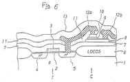
- a semiconductor non-volatile memory cell having a storage capacitor with the use of a ferroelectric comprises a structure, for instance, as shown in Fig. 6.
- This memory cell is made by connecting in series a single transfer gate transistor (MOS transistor) T to a storage capacitor (condenser) C with the use of a ferroelectric film.
- the transfer gate transistor T comprises a polysilicon gate 3 formed on a p-type semiconductor substrate 1 via a gate insulating film 2, and source and drain regions 4 and 5 as high concentration n-type regions formed by self-aligning on the surface side of the p-type semiconductor substrate 1 with the use of the polycrystalline silicon gate 3 as a mask.
- the source-drain region 4 is connected to a bit line and the polycrystalline silicon gate 3 is connected to a word line, respectively.
- the storage capacitor C is constructed on a LOCOS (local oxidized film) 6 as a field oxide film.
- LOCOS local oxidized film
- the LOCOS 6 and the polycrystalline silicon gate 3 is formed a first interlayer insulating film 7 of SiO2 by CVD or SiN by sputtering method, in this interlayer insulating film 7, a lower plate electrode 8 of platinum (Pt) right above the LOCOS 6 by sputtering method.
- a second interlayer insulating film 11 of SiO2 by CVD or SiN2 by sputtering method for instance is formed on the interlayer insulating film 11 .
- the Al wiring 12a is an inner cell wiring for conducting the source-drain region 5 and the upper plate electrode 10 via a contact hole
- the Al wiring 12b is an earth wiring conducting the lower plate electrode 8 and a pad portion (not shown).
- the word line conducting the polycrystalline silicon gate 3 and the bit dine conducting the source-drain region 4 are formed on the same layer of the above Al wiring.
- a passivation film 13 of SiN is formed on the Al wirings 12a and 12b.
- PZT Pb(Ti x Zr y )O3
- PZT Pb(Ti x Zr y )O3
- its dielectric constant is a value of about 1000 which is more than two order larger than the SiO2 film.
- the second interlayer insulating film 11 and the passivation film 13 are SiN films by sputtering method. This is because of film forming by the step of emitting no hydrogen.
- the passivation film 13 essentially requires humidity-resisting dense film quality, but the SiN film by sputtering method lacks film denseness and is poor in humidity resistance, and is inconvenient as a passivation film.
- the invention is to solve the above problems, and the task thereof is to provide a semiconductor device and a method of manufacturing the same requiring a ferroelectric film having high residual polarization and dielectric constant by employing a method for forming a film on the upper portion of a ferroelectric film for preventing hydrogen from entering into the ferroelectric film.
- means provided by the invention is to provide a humidity-resisting hydrogen barrier film on the upper portion of a ferroelectric film formed by a sputtering method or a method of application by a hydrogen non-emissible film forming method.
- a coating range of this hydrogen barrier film is not only limited to the whole surface but also preferably within a range coating a capacitor structure.
- the hydrogen barrier film use may preferably made of a TiN film by a sputtering method or oxygen penetration type TiON.
- TiON As a method of forming a TiON film, there are plasma treatment or heat treatment of a TiN film in oxygen atmosphere, a sputtering method in nitrogen or oxygen atmosphere by Ti target and a sputtering method of TiON.
- TiON is conductive when oxygen content is small and insulating when oxygen content is large.
- a TiON film having high oxygen content is high in oxygen stopping power.
- the above manufacturing methods are widely used means, but in case of forming an insulating (large oxygen content) TiON film as a hydrogen barrier film, the above step of forming a corrosion-resisting film can be reduced.
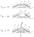
- Fig. 1 is a cross section showing a structure of a semiconductor memory relating to a first embodiment of the invention.
- Fig. 2 is a cross section showing a structure of a semiconductor memory relating to a second embodiment of the invention.
- Fig. 3 is a cross section showing a structure of a semiconductor memory relating to a third embodiment of the invention.
- Figs. 4(A) to (C) are flow sheets showing a general connecting method of a pad portion and a bonding wire in the semiconductor memory.
- Figs. 5(A) to (E) are flow sheets showing an improved connecting method of a pad portion and a bonding wire in the semiconductor memory.
- Fig. 6 is a cross section showing an embodiment of a prior semiconductor memory.
- Fig. 1 is a cross section showing a semiconductor memory relating to a first embodiment of the invention.
- a gate insulating film 2 by thermal oxidation and LOCOS (local oxide film) 6 of a thick oxide film for dividing and forming an active region of MOS On the surface of a p-type semiconductor substrate 1 are formed a gate insulating film 2 by thermal oxidation and LOCOS (local oxide film) 6 of a thick oxide film for dividing and forming an active region of MOS.
- a transfer transistor T comprises a polycrystalline silicon gate 3 formed via the gate insulating film 2 and source-drain regions 4 and 5 as high concentration n-type regions formed on the surface side of the p-type semiconductor substrate 1 with the use of the polycrystalline silicon gate 3 as a mask by self-alignment.
- a storage capacitor C is constructed on the LOCOS (local oxide film) 6 as a field oxide film.
- a dense first interlayer insulating film (SiO3 or SiN) 7 by CVD is formed on the interlayer insulating film 7 just above the LOCOS 6 .
- a lower plate electrode 8 of platinum (Pt) is formed on the interlayer insulating film 7 just above the LOCOS 6 .
- a dielectric film 9 of PZT (Pb(Ti x Zr y )O3) is formed on a part of the lower plate electrode 8 as a ferroelectric by a sputtering method or a method of application.
- an upper plate electrode 10 of platinum is formed on the dielectric film 9 a sputtering method and a storage capacitor C is obtained.
- a second interlayer insulating film (lower interlayer insulating film) 11 of SiN is formed on the first interlayer insulating film 7 by a sputtering method. Then, a contact hole is bored at the positions of the source-drain region 5, the upper plate electrode 10 and the lower plate electrode 8.
- the Al wiring 12a is a cell interior wiring connecting the source-drain region 5 and the upper plate electrode 10 via the contact hole
- the Al wiring 12b is an earth wiring connecting the lower plate electrode 8 and a pad portion (not shown).
- a word line connecting to the polycrystalline silicon gate 3 and a bit line connecting to the source-drain region 4 are formed on the same layer as the Al wiring.
- a third interlayer insulating film (upper interlayer insulating film) 13' of SiN by a sputtering method. It is a matter of course that hydrogen is not emitted in this process, so that there is no problem of property deterioration of the dielectric film 9.
- the third interlayer insulating film 13' lacks denseness and fed significance as a passivation film, as stated later on, and has significance as an interlayer insulating film between a conductive humidity-resisting hydrogen barrier 14 and the Al wirings 12a, 12b.
- a TiN film as a humidity-resisting hydrogen barrier film 14 by a sputtering method.
- hydrogen is not generated and a problem of property deterioration of the dielectric film 9 does not occur.
- the inventor has found that this TiN film is preferable as a hydrogen barrier film 14.
- the TiN film is known as barrier metal of silicon and Al, but this TiN film is rich in denseness and a conductive film, so that it is a humidity-resisting hydrogen non-permeable protective film and simultaneously performs an electromagnetic shield function.
- This titanium nitride (TiN) is liable to be oxidized to be oxygen penetration type TiO.
- TiON having high oxygen content has higher oxygen non-permeability and is excellent as a hydrogen barrier film. Therefore, as this hydrogen barrier film 14, a TiON film may be preferable.
- a method of forming a TiON film either one of the following methods is employed.
- the hydrogen barrier film 14 is a TiN film or a TiON film and has conductivity in general, but oxygen penetration type TiON has conductivity when oxygen content is small and has insulation properties when oxygen content is large.
- Fig. 2 is a cross section showing a semiconductor memory relating to a second embodiment of the invention. Moreover, like parts shown in Fig. 1 are represented by like reference symbols in Fig. 2 and the explanation is omitted.
- an SiN film by a plasma CVD method or a corrosion-resistant film 15 of an SiO2 film by a normal pressure or reduced pressure CVD method is rich in denseness and prevents penetration of humidity, so as to prevent corrosion of the hydrogen barrier film 14.
- the method of forming the SiN film by A plasma CVD method or the SiO2 film by a normal pressure or reduced pressure CVD method is a process in generation of hydrogen or a hydrogen atmosphere, but the hydrogen penetration is prevented by the already formed hydrogen barrier film 14, and does not cause an influence upon the dielectric film 9.
- Fig. 3 is a cross section of a semiconductor memory relating to a third embodiment of the invention. Moreover, like parts shown in Fig. 2 are represented by like reference symbols in Fig. 3 and the explanation is omitted.
- a different point of this third embodiment from the second embodiment is to limit the formation region of a hydrogen barrier film 14' of a TiN film or TiON film to a range covering a storage capacity structure.
- Significance of the hydrogen barrier film 14' lies in humidity resistance, and may preferably be in hydrogen non-penetration and hydrogen non-permeability.
- a corrosion-resisting film 15 of an SiN film by a plasma CVD method or an SiO2 film by a normal pressure or reduced pressure CVD method on the hydrogen barrier film 14' invites generation of hydrogen in the film, but even if hydrogen penetrates into the sublayer of a laminated structure, if the hydrogen barrier film 14' shields hydrogen penetration for preventing hydrogen from reaching to the dielectric film 9, it is sufficient.
- the hydrogen barrier film 14' shields hydrogen penetration within a range covering the storage capacitor structure. A hydrogen penetration through from the lateral direction is almost no problem.
- the totally formed hydrogen barrier film 14 is a TiN film or a TiON film having small oxygen content
- the film is conductive, so that it is necessary to consider a method of connecting a pad portion formed on the same layer as the Al wiring 12b and a bonding wire.
- a general connecting method is shown in Fig. 4. First, as shown in Fig. 4(A), three layers just above an Al pad portion 12c are removed by an etching treatment and a contact hole 16 is formed, and then as shown in Fig. 4(C), a bonding wire 17 is pressed to an exposed region of the Al pad portion 12c. According to such connecting method, the bonding wire 17 can be connected to not only the Al pad portion 12c but also the conductive hydrogen barrier 14 facing to the side wall of the contact hole.
- Fig. 5 is a flow sheet showing an improved connecting method of a pad portion and a bonding wire in order to solve the above problem.
- a second interlayer insulating film is formed an Al pad portion 12c with the same layer as the Al wiring 12b, on which are successively formed a second interlayer insulating film 13' and a conductive hydrogen barrier film 14.
- a corrosion-resisting film 15' on the hydrogen barrier film 14 inclusive of the above exposed region X is formed a corrosion-resisting film 15'.
- the inside of the contact hole 16a is covered with the corrosion-resisting film 15'.
- one layer of the corrosion-resisting film 15 just above the Al pad portion 12c is removed by etching and a contact hole 16b is formed.
- a range Y of the exposed region formed on the surface of the Al pad portion 12c is narrowly set as compared with a range X of the above exposed region.
- a bonding wire 17 is pressed to the exposed region Y of the Al pad portion 12c.
- the bonding wire 17 becomes conductive only to the Al pad portion 12c but is not conductive to the conductive hydrogen barrier film 14. Because the hydrogen barrier film 14 and the bonding wire 17 are insulated by the corrosion-resisting film 15. Moreover, the above connecting method can be applied to connection of the Al pad portion 12 and a bump, and connection of the Al wiring and Al of the upper layer (through-hole connection).
- the problem of property deterioration by hydrogen penetration is caused not only in ferroelectric film, but also in CMOS integrated circuit having a polycrystalline silicon gate. If a polycrystalline silicon gate touches hydrogen, the change of a threshold value is invited to be a factor for worsening yield. Therefore, formation of a humidity-resistant hydrogen barrier film as a protective film of a ferroelectric film and a polycrystalline silicon gate contributes to stability of properties of the polycrystalline silicon gate.
- the invention has a characteristic in the point of forming a humidity-resistant hydrogen barrier film such as a TiN film, TiON film and the like on the upper portion of a ferroelectric or a polycrystalline silicon gate by a hydrogen non-emission film forming method in a semiconductor device which element is the ferroelectric or polycrystalline silicon gate. Therefore, the following effects are performed.
Landscapes
- Semiconductor Memories (AREA)
- Semiconductor Integrated Circuits (AREA)
- Metal-Oxide And Bipolar Metal-Oxide Semiconductor Integrated Circuits (AREA)
- Formation Of Insulating Films (AREA)
- Internal Circuitry In Semiconductor Integrated Circuit Devices (AREA)
- Non-Volatile Memory (AREA)
Abstract
Applications Claiming Priority (3)
| Application Number | Priority Date | Filing Date | Title |
|---|---|---|---|
| JP02220905A JP3131982B2 (ja) | 1990-08-21 | 1990-08-21 | 半導体装置、半導体メモリ及び半導体装置の製造方法 |
| JP220905/90 | 1990-08-21 | ||
| PCT/JP1991/001105 WO1992003849A1 (fr) | 1990-08-21 | 1991-08-20 | Dispositif a semi-conducteur, memoire a semi-conducteur l'utilisant, circuit integre a semi-conducteur cmos et procede de production de ce dispositif |
Publications (3)
| Publication Number | Publication Date |
|---|---|
| EP0514547A4 EP0514547A4 (fr) | 1992-09-10 |
| EP0514547A1 true EP0514547A1 (fr) | 1992-11-25 |
| EP0514547B1 EP0514547B1 (fr) | 1997-03-05 |
Family
ID=16758373
Family Applications (1)
| Application Number | Title | Priority Date | Filing Date |
|---|---|---|---|
| EP91914601A Expired - Lifetime EP0514547B1 (fr) | 1990-08-21 | 1991-08-20 | MEMOIRE A SEMI-CONDUCTEUR UTILISANT UN CONDENSATEUR FERROELECTRIQUE ET UNE COUCHE DE PROTECTION DE TiON |
Country Status (5)
| Country | Link |
|---|---|
| US (1) | US5523595A (fr) |
| EP (1) | EP0514547B1 (fr) |
| JP (1) | JP3131982B2 (fr) |
| DE (1) | DE69124994T2 (fr) |
| WO (1) | WO1992003849A1 (fr) |
Cited By (14)
| Publication number | Priority date | Publication date | Assignee | Title |
|---|---|---|---|---|
| EP0513894A3 (en) * | 1991-05-08 | 1993-05-26 | N.V. Philips' Gloeilampenfabrieken | Method of manufacturing a semiconductor device comprising a capacitor with a ferroelectric dielectric, and semiconductor device comprising such a capacitor |
| EP0642167A3 (fr) * | 1993-08-05 | 1995-06-28 | Matsushita Electronics Corp | Dispositif semi-conducteur avec capacité et son procédé de fabrication. |
| EP0671765A1 (fr) * | 1994-03-11 | 1995-09-13 | Ramtron International Corporation | Procédé de passivation et structure de circuit intégré ferroélectrique utilisant des matériaux céramiques durs ou d'autres matériaux |
| EP0689236A1 (fr) * | 1994-06-21 | 1995-12-27 | Matsushita Electronics Corporation | Dispositif à semi-conducteur ayant un élément capacitif et procédé pour sa fabrication |
| EP0877422A1 (fr) * | 1997-05-09 | 1998-11-11 | Ramtron International Corporation | Procédé de métallisation à deux niveaux pour les dispositifs ferroélectriques à circuit intégré |
| EP0920061A3 (fr) * | 1997-11-26 | 1999-11-03 | Nec Corporation | Capacité et dispositif de mémoire correspondant, et méthode de fabrication de ceux-ci |
| EP0994511A1 (fr) | 1998-10-12 | 2000-04-19 | Sony Corporation | Dispositif semi-conducteur et son procédé de fabrication |
| GB2358287A (en) * | 1999-09-10 | 2001-07-18 | Samsung Electronics Co Ltd | DRAM device having a multilayer capacitor encapsulation layer |
| EP1142016A1 (fr) * | 1998-11-13 | 2001-10-10 | Infineon Technologies AG | Resistance en polysilicium et son procede de production |
| WO2002056382A1 (fr) * | 2001-01-15 | 2002-07-18 | Matsushita Electric Industrial Co., Ltd. | Dispositif semiconducteur et procede de fabrication dudit dispositif |
| US6509601B1 (en) | 1998-07-31 | 2003-01-21 | Samsung Electronics Co., Ltd. | Semiconductor memory device having capacitor protection layer and method for manufacturing the same |
| DE10303316A1 (de) * | 2003-01-28 | 2004-08-12 | Forschungszentrum Jülich GmbH | Schneller remanenter Speicher |
| DE4426121B4 (de) * | 1993-07-23 | 2005-11-03 | Hyundai Electronics Industries Co., Ltd., Ichon | Verfahren zur Herstellung einer Halbleiterspeichervorrichtung |
| US8772917B2 (en) | 2006-02-10 | 2014-07-08 | Semiconductor Energy Laboratory Co., Ltd. | Semiconductor device having an antenna |
Families Citing this family (54)
| Publication number | Priority date | Publication date | Assignee | Title |
|---|---|---|---|---|
| US5719416A (en) * | 1991-12-13 | 1998-02-17 | Symetrix Corporation | Integrated circuit with layered superlattice material compound |
| DE69317940T2 (de) * | 1992-06-12 | 1998-11-26 | Matsushita Electronics Corp., Takatsuki, Osaka | Halbleiterbauelement mit Kondensator |
| JP3195828B2 (ja) * | 1992-08-31 | 2001-08-06 | 三菱電機株式会社 | 半導体装置 |
| KR100407232B1 (ko) * | 1992-10-23 | 2004-06-26 | 시메트릭스 코포레이션 | 직접회로와이직접회로의제조방법 |
| JPH09260600A (ja) * | 1996-03-19 | 1997-10-03 | Sharp Corp | 半導体メモリ素子の製造方法 |
| DE19640240A1 (de) * | 1996-09-30 | 1998-04-02 | Siemens Ag | Halbleiteranordnung mit einer Schicht aus einem Edelmetall und Verfahren zum Herstellen derselben |
| JP3385889B2 (ja) * | 1996-12-25 | 2003-03-10 | 株式会社日立製作所 | 強誘電体メモリ素子及びその製造方法 |
| JP4500248B2 (ja) * | 1997-01-13 | 2010-07-14 | 株式会社ルネサステクノロジ | 半導体記憶装置 |
| JP3257587B2 (ja) | 1997-05-23 | 2002-02-18 | 日本電気株式会社 | 誘電体膜を用いた半導体装置の製造方法 |
| JPH118355A (ja) * | 1997-06-16 | 1999-01-12 | Nec Corp | 強誘電体メモリ |
| TW396454B (en) | 1997-06-24 | 2000-07-01 | Matsushita Electrics Corporati | Semiconductor device and method for fabricating the same |
| KR19990003495A (ko) * | 1997-06-25 | 1999-01-15 | 김영환 | 반도체 소자의 베리어 금속층 형성방법 |
| JP3098474B2 (ja) | 1997-10-31 | 2000-10-16 | 日本電気株式会社 | 半導体装置の製造方法 |
| KR100533991B1 (ko) | 1997-12-27 | 2006-05-16 | 주식회사 하이닉스반도체 | 반도체 장치의 고유전체 캐패시터 제조방법 |
| JP3698885B2 (ja) * | 1998-02-18 | 2005-09-21 | 富士通株式会社 | 強誘電体膜を用いた装置の製造方法 |
| US6225156B1 (en) | 1998-04-17 | 2001-05-01 | Symetrix Corporation | Ferroelectric integrated circuit having low sensitivity to hydrogen exposure and method for fabricating same |
| US6207465B1 (en) | 1998-04-17 | 2001-03-27 | Symetrix Corporation | Method of fabricating ferroelectric integrated circuit using dry and wet etching |
| US6130103A (en) * | 1998-04-17 | 2000-10-10 | Symetrix Corporation | Method for fabricating ferroelectric integrated circuits |
| US6165802A (en) * | 1998-04-17 | 2000-12-26 | Symetrix Corporation | Method of fabricating ferroelectric integrated circuit using oxygen to inhibit and repair hydrogen degradation |
| US6512256B1 (en) | 1998-11-20 | 2003-01-28 | Symetrix Corporation | Integrated circuit having self-aligned hydrogen barrier layer and method for fabricating same |
| US6225656B1 (en) * | 1998-12-01 | 2001-05-01 | Symetrix Corporation | Ferroelectric integrated circuit with protective layer incorporating oxygen and method for fabricating same |
| JP3276007B2 (ja) * | 1999-07-02 | 2002-04-22 | 日本電気株式会社 | 混載lsi半導体装置 |
| US6140672A (en) * | 1999-03-05 | 2000-10-31 | Symetrix Corporation | Ferroelectric field effect transistor having a gate electrode being electrically connected to the bottom electrode of a ferroelectric capacitor |
| JP3217326B2 (ja) | 1999-03-19 | 2001-10-09 | 富士通株式会社 | 電磁波シールド構造を有する強誘電体メモリ |
| US6242299B1 (en) | 1999-04-01 | 2001-06-05 | Ramtron International Corporation | Barrier layer to protect a ferroelectric capacitor after contact has been made to the capacitor electrode |
| US6611014B1 (en) | 1999-05-14 | 2003-08-26 | Kabushiki Kaisha Toshiba | Semiconductor device having ferroelectric capacitor and hydrogen barrier film and manufacturing method thereof |
| JP2002280528A (ja) * | 1999-05-14 | 2002-09-27 | Toshiba Corp | 半導体装置及びその製造方法 |
| JP4031158B2 (ja) * | 1999-09-27 | 2008-01-09 | 株式会社東芝 | 半導体装置 |
| KR100362189B1 (ko) * | 1999-12-30 | 2002-11-23 | 주식회사 하이닉스반도체 | 수소 확산을 방지할 수 있는 산화막 및 티타늄막 이중층을구비하는 반도체 메모리 소자 및 그 제조 방법 |
| DE10000005C1 (de) | 2000-01-03 | 2001-09-13 | Infineon Technologies Ag | Verfahren zur Herstellung eines ferroelektrischen Halbleiterspeichers |
| DE10065976A1 (de) | 2000-02-25 | 2002-02-21 | Infineon Technologies Ag | Verfahren zur Herstellung eines Halbleiterbauelements |
| US6365927B1 (en) | 2000-04-03 | 2002-04-02 | Symetrix Corporation | Ferroelectric integrated circuit having hydrogen barrier layer |
| IT1318279B1 (it) * | 2000-07-28 | 2003-07-28 | Getters Spa | Dispositivo capacitivo integrato con strato dielettrico degradabiledall'idrogeno protetto da strato getter. |
| US6580107B2 (en) * | 2000-10-10 | 2003-06-17 | Sanyo Electric Co., Ltd. | Compound semiconductor device with depletion layer stop region |
| JP2002305289A (ja) * | 2001-04-05 | 2002-10-18 | Hitachi Ltd | 半導体集積回路装置およびその製造方法 |
| DE10121657B4 (de) | 2001-05-03 | 2010-02-11 | Qimonda Ag | Mikroelektronische Struktur mit Wasserstoffbarrierenschicht |
| WO2002093906A1 (fr) * | 2001-05-15 | 2002-11-21 | Ebara Corporation | Dispositif de detection tdi, equipement d'entree et appareil a faisceau d'electrons comprenant ces dispositifs. |
| US6762090B2 (en) | 2001-09-13 | 2004-07-13 | Hynix Semiconductor Inc. | Method for fabricating a capacitor |
| JP4488661B2 (ja) * | 2001-09-18 | 2010-06-23 | Okiセミコンダクタ株式会社 | 強誘電体キャパシタの製造方法 |
| JP3466174B2 (ja) | 2001-09-27 | 2003-11-10 | 沖電気工業株式会社 | 半導体装置およびその製造方法 |
| KR100989083B1 (ko) | 2005-07-04 | 2010-10-25 | 후지쯔 세미컨덕터 가부시키가이샤 | 반도체 장치 및 그 제조 방법 |
| JP4998262B2 (ja) * | 2005-07-05 | 2012-08-15 | 富士通セミコンダクター株式会社 | 半導体装置及びその製造方法 |
| JP4854675B2 (ja) * | 2005-11-28 | 2012-01-18 | 富士通セミコンダクター株式会社 | 半導体装置及びその製造方法 |
| JP4998270B2 (ja) * | 2005-12-27 | 2012-08-15 | 富士通セミコンダクター株式会社 | 半導体装置とその製造方法 |
| WO2007116501A1 (fr) * | 2006-03-31 | 2007-10-18 | Fujitsu Limited | Dispositif a semi-conducteurs et son procede de fabrication |
| US8723654B2 (en) | 2010-07-09 | 2014-05-13 | Cypress Semiconductor Corporation | Interrupt generation and acknowledgment for RFID |
| US9846664B2 (en) | 2010-07-09 | 2017-12-19 | Cypress Semiconductor Corporation | RFID interface and interrupt |
| US9092582B2 (en) | 2010-07-09 | 2015-07-28 | Cypress Semiconductor Corporation | Low power, low pin count interface for an RFID transponder |
| PT2627659T (pt) * | 2010-10-15 | 2016-07-25 | Upm Kymmene Corp | Método contínuo para a precipitação de lignina a partir do licor negro |
| US8395196B2 (en) | 2010-11-16 | 2013-03-12 | International Business Machines Corporation | Hydrogen barrier liner for ferro-electric random access memory (FRAM) chip |
| US8525354B2 (en) * | 2011-10-13 | 2013-09-03 | United Microelectronics Corporation | Bond pad structure and fabricating method thereof |
| US20130328151A1 (en) * | 2012-06-07 | 2013-12-12 | Ching-Hung Kao | Integrated circuit structure, back side illumination image sensor and integrated circuit process thereof |
| CN103578919A (zh) * | 2012-07-26 | 2014-02-12 | 无锡华润上华科技有限公司 | 一种mos器件的钝化层形成方法以及一种mos器件 |
| JP2016058601A (ja) * | 2014-09-11 | 2016-04-21 | 株式会社東芝 | 半導体装置 |
Family Cites Families (17)
| Publication number | Priority date | Publication date | Assignee | Title |
|---|---|---|---|---|
| JPS5748247A (en) * | 1980-09-05 | 1982-03-19 | Oki Electric Ind Co Ltd | Semiconductor integrated circuit device |
| JPS59105364A (ja) * | 1982-12-08 | 1984-06-18 | Hitachi Ltd | 半導体装置 |
| US4675715A (en) * | 1982-12-09 | 1987-06-23 | American Telephone And Telegraph Company, At&T Bell Laboratories | Semiconductor integrated circuit vertical geometry impedance element |
| JPS59110122A (ja) * | 1982-12-15 | 1984-06-26 | Nec Corp | 窒化膜を有する半導体集積回路装置 |
| JPS60100464A (ja) * | 1983-11-07 | 1985-06-04 | Hitachi Ltd | 半導体装置 |
| US4811078A (en) * | 1985-05-01 | 1989-03-07 | Texas Instruments Incorporated | Integrated circuit device and process with tin capacitors |
| JPS6223149A (ja) * | 1985-07-24 | 1987-01-31 | Hitachi Ltd | 半導体記憶装置 |
| JPS6328069A (ja) * | 1986-07-22 | 1988-02-05 | Seiko Epson Corp | 半導体装置 |
| JPH01225149A (ja) * | 1988-03-04 | 1989-09-08 | Toshiba Corp | キャパシタ及びその製造方法 |
| JP2681982B2 (ja) * | 1988-03-23 | 1997-11-26 | ソニー株式会社 | 半導体装置 |
| JPH01253257A (ja) * | 1988-04-01 | 1989-10-09 | Fuji Electric Co Ltd | 半導体集積デバイス |
| JPH01265524A (ja) * | 1988-04-15 | 1989-10-23 | Sony Corp | 半導体装置 |
| US5070036A (en) * | 1989-01-04 | 1991-12-03 | Quality Microcircuits Corporation | Process for contacting and interconnecting semiconductor devices within an integrated circuit |
| JP2697062B2 (ja) * | 1989-01-09 | 1998-01-14 | 日本電気株式会社 | 半導体装置の製造方法 |
| JPH02184079A (ja) * | 1989-01-11 | 1990-07-18 | Seiko Epson Corp | 強誘電体記憶装置の形成法 |
| JPH03173126A (ja) * | 1989-11-30 | 1991-07-26 | Mitsubishi Electric Corp | 多層膜構造の半導体装置およびその製造方法 |
| US5119154A (en) * | 1990-12-03 | 1992-06-02 | Micron Technology, Inc. | Ferroelectric capacitor and method for forming local interconnect |
-
1990
- 1990-08-21 JP JP02220905A patent/JP3131982B2/ja not_active Expired - Lifetime
-
1991
- 1991-08-20 WO PCT/JP1991/001105 patent/WO1992003849A1/fr not_active Ceased
- 1991-08-20 DE DE69124994T patent/DE69124994T2/de not_active Expired - Fee Related
- 1991-08-20 EP EP91914601A patent/EP0514547B1/fr not_active Expired - Lifetime
-
1994
- 1994-05-06 US US08/238,802 patent/US5523595A/en not_active Expired - Lifetime
Cited By (32)
| Publication number | Priority date | Publication date | Assignee | Title |
|---|---|---|---|---|
| EP0513894A3 (en) * | 1991-05-08 | 1993-05-26 | N.V. Philips' Gloeilampenfabrieken | Method of manufacturing a semiconductor device comprising a capacitor with a ferroelectric dielectric, and semiconductor device comprising such a capacitor |
| DE4426121B4 (de) * | 1993-07-23 | 2005-11-03 | Hyundai Electronics Industries Co., Ltd., Ichon | Verfahren zur Herstellung einer Halbleiterspeichervorrichtung |
| US6015987A (en) * | 1993-08-05 | 2000-01-18 | Matsushita Electric Industrial Co., Ltd. | Semiconductor device having capacitor exhibiting improved mositure resistance and manufacturing method thereof |
| US6333528B1 (en) | 1993-08-05 | 2001-12-25 | Matsushita Electric Industrial Co., Ltd. | Semiconductor device having a capacitor exhibiting improved moisture resistance |
| US5624864A (en) * | 1993-08-05 | 1997-04-29 | Matsushita Electronics Corporation | Semiconductor device having capacitor and manufacturing method thereof |
| EP0642167A3 (fr) * | 1993-08-05 | 1995-06-28 | Matsushita Electronics Corp | Dispositif semi-conducteur avec capacité et son procédé de fabrication. |
| EP0738009A3 (fr) * | 1993-08-05 | 1998-04-15 | Matsushita Electronics Corporation | Dispositif semi-conducteur avec un condensateur |
| EP0739037A3 (fr) * | 1993-08-05 | 1998-04-29 | Matsushita Electronics Corporation | Dispositif semi-conducteur avec un condensateur et son procédé de fabrication |
| US6169304B1 (en) | 1993-08-05 | 2001-01-02 | Matsushita Electric Industrial Co., Ltd. | Semiconductor device having a passivation layer which minimizes diffusion of hydrogen into a dielectric layer |
| US6107657A (en) * | 1993-08-05 | 2000-08-22 | Matsushita Electronics Corporation | Semiconductor device having capacitor and manufacturing method thereof |
| US6294438B1 (en) | 1993-08-05 | 2001-09-25 | Matsushita Electronics Corporation | Semiconductor device having capacitor and manufacturing method thereof |
| US5578867A (en) * | 1994-03-11 | 1996-11-26 | Ramtron International Corporation | Passivation method and structure using hard ceramic materials or the like |
| EP0671765A1 (fr) * | 1994-03-11 | 1995-09-13 | Ramtron International Corporation | Procédé de passivation et structure de circuit intégré ferroélectrique utilisant des matériaux céramiques durs ou d'autres matériaux |
| US5644158A (en) * | 1994-06-21 | 1997-07-01 | Matsushita Electronics Corporation | Semiconductor memory device reducing hydrogen content |
| EP0689236A1 (fr) * | 1994-06-21 | 1995-12-27 | Matsushita Electronics Corporation | Dispositif à semi-conducteur ayant un élément capacitif et procédé pour sa fabrication |
| US5902131A (en) * | 1997-05-09 | 1999-05-11 | Ramtron International Corporation | Dual-level metalization method for integrated circuit ferroelectric devices |
| EP0877422A1 (fr) * | 1997-05-09 | 1998-11-11 | Ramtron International Corporation | Procédé de métallisation à deux niveaux pour les dispositifs ferroélectriques à circuit intégré |
| US6180971B1 (en) | 1997-11-26 | 2001-01-30 | Symetrix Corporation | Capacitor and method of manufacturing the same |
| US6455327B1 (en) | 1997-11-26 | 2002-09-24 | Symetrix Corporation | Method of manufacturing a ferroelectric capacitor |
| EP0920061A3 (fr) * | 1997-11-26 | 1999-11-03 | Nec Corporation | Capacité et dispositif de mémoire correspondant, et méthode de fabrication de ceux-ci |
| US6509601B1 (en) | 1998-07-31 | 2003-01-21 | Samsung Electronics Co., Ltd. | Semiconductor memory device having capacitor protection layer and method for manufacturing the same |
| US6548873B2 (en) | 1998-10-12 | 2003-04-15 | Sony Corporation | Semiconductor device and manufacturing method of the same |
| EP0994511A1 (fr) | 1998-10-12 | 2000-04-19 | Sony Corporation | Dispositif semi-conducteur et son procédé de fabrication |
| EP1142016A1 (fr) * | 1998-11-13 | 2001-10-10 | Infineon Technologies AG | Resistance en polysilicium et son procede de production |
| GB2358287A (en) * | 1999-09-10 | 2001-07-18 | Samsung Electronics Co Ltd | DRAM device having a multilayer capacitor encapsulation layer |
| GB2358287B (en) * | 1999-09-10 | 2004-05-12 | Samsung Electronics Co Ltd | Semiconductor memory device having capacitor protection layer and method for manufacturing the same |
| WO2002056382A1 (fr) * | 2001-01-15 | 2002-07-18 | Matsushita Electric Industrial Co., Ltd. | Dispositif semiconducteur et procede de fabrication dudit dispositif |
| US7132709B2 (en) | 2001-01-15 | 2006-11-07 | Matsushita Electric Industrial Co., Ltd. | Semiconductor device including a capacitor having a capacitive insulating film of an insulating metal oxide |
| DE10303316A1 (de) * | 2003-01-28 | 2004-08-12 | Forschungszentrum Jülich GmbH | Schneller remanenter Speicher |
| US8772917B2 (en) | 2006-02-10 | 2014-07-08 | Semiconductor Energy Laboratory Co., Ltd. | Semiconductor device having an antenna |
| US9437777B2 (en) | 2006-02-10 | 2016-09-06 | Semiconductor Energy Laboratory Co., Ltd. | Semiconductor device with antenna and light-emitting element |
| US9768210B2 (en) | 2006-02-10 | 2017-09-19 | Semiconductor Energy Laboratory Co., Ltd. | Semiconductor device having antenna and sensor elements |
Also Published As
| Publication number | Publication date |
|---|---|
| DE69124994T2 (de) | 1997-09-25 |
| JPH04102367A (ja) | 1992-04-03 |
| US5523595A (en) | 1996-06-04 |
| JP3131982B2 (ja) | 2001-02-05 |
| WO1992003849A1 (fr) | 1992-03-05 |
| DE69124994D1 (de) | 1997-04-10 |
| EP0514547B1 (fr) | 1997-03-05 |
| EP0514547A4 (fr) | 1992-09-10 |
Similar Documents
| Publication | Publication Date | Title |
|---|---|---|
| EP0514547A1 (fr) | MEMOIRE A SEMI-CONDUCTEUR UTILISANT UN CONDENSATEUR FERROELECTRIQUE ET UNE COUCHE DE PROTECTION DE TiON | |
| US5468684A (en) | Integrated circuit with layered superlattice material and method of fabricating same | |
| US6455882B1 (en) | Semiconductor device having a hydrogen barrier layer | |
| US6020229A (en) | Semiconductor device method for manufacturing | |
| US5719416A (en) | Integrated circuit with layered superlattice material compound | |
| US6794257B2 (en) | Method of manufacturing a semiconductor integrated circuit device | |
| KR19990030200A (ko) | 커패시터와 mos 트랜지스터를 갖는 반도체 기억소자 | |
| US5498561A (en) | Method of fabricating memory cell for semiconductor integrated circuit | |
| US6043561A (en) | Electronic material, its manufacturing method, dielectric capacitor, non-volatile memory and semiconductor device | |
| KR100304673B1 (ko) | 강유전체메모리및그제조방법 | |
| JP2633584B2 (ja) | 半導体装置及びその製造方法 | |
| JP3362712B2 (ja) | 半導体装置、それを用いた半導体メモリ及びcmos半導体集積回路並びにその半導体装置の製造方法 | |
| KR100304285B1 (ko) | 확산장벽이 구비된 적층 캐패시터 | |
| US6046490A (en) | Semiconductor device having a capacitor dielectric element and wiring layers | |
| JPH07169854A (ja) | 半導体デバイスおよびその製造方法 | |
| US5414277A (en) | Thin film transistor which prevents generation of hot carriers | |
| JP2001156270A (ja) | 半導体集積回路装置およびその製造方法 | |
| JP3449298B2 (ja) | 半導体装置 | |
| JP3164105B2 (ja) | 半導体装置、それを用いた半導体メモリ及びcmos半導体集積回路並びにその半導体装置の製造方法 | |
| JP3332013B2 (ja) | 半導体装置及びその製造方法 | |
| KR100321692B1 (ko) | 강유전체 메모리 소자의 캐패시터 및 그 제조방법 | |
| JP3387454B2 (ja) | 半導体装置、半導体メモリ及び半導体装置の製造方法 | |
| JP3467566B2 (ja) | 半導体装置 | |
| KR100203301B1 (ko) | 반도체 소자의 층간 절연막 형성 방법 | |
| JPH10242407A (ja) | 容量素子及びその製造方法 |
Legal Events
| Date | Code | Title | Description |
|---|---|---|---|
| PUAI | Public reference made under article 153(3) epc to a published international application that has entered the european phase |
Free format text: ORIGINAL CODE: 0009012 |
|
| 17P | Request for examination filed |
Effective date: 19920518 |
|
| AK | Designated contracting states |
Kind code of ref document: A1 Designated state(s): DE FR GB IT NL |
|
| RAP1 | Party data changed (applicant data changed or rights of an application transferred) |
Owner name: RAMTRON INTERNATIONAL CORPORATION |
|
| 17Q | First examination report despatched |
Effective date: 19941026 |
|
| GRAG | Despatch of communication of intention to grant |
Free format text: ORIGINAL CODE: EPIDOS AGRA |
|
| GRAH | Despatch of communication of intention to grant a patent |
Free format text: ORIGINAL CODE: EPIDOS IGRA |
|
| GRAH | Despatch of communication of intention to grant a patent |
Free format text: ORIGINAL CODE: EPIDOS IGRA |
|
| GRAA | (expected) grant |
Free format text: ORIGINAL CODE: 0009210 |
|
| AK | Designated contracting states |
Kind code of ref document: B1 Designated state(s): DE FR GB IT NL |
|
| PG25 | Lapsed in a contracting state [announced via postgrant information from national office to epo] |
Ref country code: IT Free format text: LAPSE BECAUSE OF FAILURE TO SUBMIT A TRANSLATION OF THE DESCRIPTION OR TO PAY THE FEE WITHIN THE PRE;WARNING: LAPSES OF ITALIAN PATENTS WITH EFFECTIVE DATE BEFORE 2007 MAY HAVE OCCURRED AT ANY TIME BEFORE 2007. THE CORRECT EFFECTIVE DATE MAY BE DIFFERENT FROM THE ONE RECORDED.SCRIBED TIME-LIMIT Effective date: 19970305 Ref country code: FR Effective date: 19970305 Ref country code: NL Free format text: LAPSE BECAUSE OF FAILURE TO SUBMIT A TRANSLATION OF THE DESCRIPTION OR TO PAY THE FEE WITHIN THE PRESCRIBED TIME-LIMIT Effective date: 19970305 |
|
| REF | Corresponds to: |
Ref document number: 69124994 Country of ref document: DE Date of ref document: 19970410 |
|
| EN | Fr: translation not filed | ||
| NLV1 | Nl: lapsed or annulled due to failure to fulfill the requirements of art. 29p and 29m of the patents act | ||
| PLBE | No opposition filed within time limit |
Free format text: ORIGINAL CODE: 0009261 |
|
| STAA | Information on the status of an ep patent application or granted ep patent |
Free format text: STATUS: NO OPPOSITION FILED WITHIN TIME LIMIT |
|
| 26N | No opposition filed | ||
| REG | Reference to a national code |
Ref country code: GB Ref legal event code: 732E |
|
| PGFP | Annual fee paid to national office [announced via postgrant information from national office to epo] |
Ref country code: DE Payment date: 20010813 Year of fee payment: 11 |
|
| PGFP | Annual fee paid to national office [announced via postgrant information from national office to epo] |
Ref country code: GB Payment date: 20010815 Year of fee payment: 11 |
|
| REG | Reference to a national code |
Ref country code: GB Ref legal event code: IF02 |
|
| PG25 | Lapsed in a contracting state [announced via postgrant information from national office to epo] |
Ref country code: GB Free format text: LAPSE BECAUSE OF NON-PAYMENT OF DUE FEES Effective date: 20020820 |
|
| PG25 | Lapsed in a contracting state [announced via postgrant information from national office to epo] |
Ref country code: DE Free format text: LAPSE BECAUSE OF NON-PAYMENT OF DUE FEES Effective date: 20030301 |
|
| GBPC | Gb: european patent ceased through non-payment of renewal fee |
Effective date: 20020820 |