EP0520093B1 - Conversion parallèle-série de données d'information - Google Patents
Conversion parallèle-série de données d'information Download PDFInfo
- Publication number
- EP0520093B1 EP0520093B1 EP91201608A EP91201608A EP0520093B1 EP 0520093 B1 EP0520093 B1 EP 0520093B1 EP 91201608 A EP91201608 A EP 91201608A EP 91201608 A EP91201608 A EP 91201608A EP 0520093 B1 EP0520093 B1 EP 0520093B1
- Authority
- EP
- European Patent Office
- Prior art keywords
- zero
- signals
- line
- level
- image
- Prior art date
- Legal status (The legal status is an assumption and is not a legal conclusion. Google has not performed a legal analysis and makes no representation as to the accuracy of the status listed.)
- Expired - Lifetime
Links
- 238000006243 chemical reaction Methods 0.000 title claims description 23
- 238000000034 method Methods 0.000 claims description 32
- 238000007639 printing Methods 0.000 claims description 21
- 230000009467 reduction Effects 0.000 claims description 4
- 239000003086 colorant Substances 0.000 claims 2
- 238000010438 heat treatment Methods 0.000 description 23
- 238000007651 thermal printing Methods 0.000 description 9
- 238000010586 diagram Methods 0.000 description 7
- 230000008569 process Effects 0.000 description 4
- 238000010276 construction Methods 0.000 description 3
- 238000010023 transfer printing Methods 0.000 description 3
- 238000012937 correction Methods 0.000 description 2
- 238000001514 detection method Methods 0.000 description 2
- 230000000694 effects Effects 0.000 description 2
- 230000006870 function Effects 0.000 description 2
- 230000010354 integration Effects 0.000 description 2
- 230000003287 optical effect Effects 0.000 description 2
- 238000002360 preparation method Methods 0.000 description 2
- 238000000926 separation method Methods 0.000 description 2
- 239000002131 composite material Substances 0.000 description 1
- 239000013078 crystal Substances 0.000 description 1
- 230000001186 cumulative effect Effects 0.000 description 1
- 230000001419 dependent effect Effects 0.000 description 1
- 238000009792 diffusion process Methods 0.000 description 1
- 238000005516 engineering process Methods 0.000 description 1
- 230000020169 heat generation Effects 0.000 description 1
- 238000003702 image correction Methods 0.000 description 1
- 238000007641 inkjet printing Methods 0.000 description 1
- 230000003134 recirculating effect Effects 0.000 description 1
- 238000009877 rendering Methods 0.000 description 1
- 230000004044 response Effects 0.000 description 1
- 230000001235 sensitizing effect Effects 0.000 description 1
- 239000004753 textile Substances 0.000 description 1
- 238000012795 verification Methods 0.000 description 1
- 238000010792 warming Methods 0.000 description 1
Images


Classifications
-
- H—ELECTRICITY
- H03—ELECTRONIC CIRCUITRY
- H03M—CODING; DECODING; CODE CONVERSION IN GENERAL
- H03M9/00—Parallel/series conversion or vice versa
-
- H—ELECTRICITY
- H04—ELECTRIC COMMUNICATION TECHNIQUE
- H04N—PICTORIAL COMMUNICATION, e.g. TELEVISION
- H04N1/00—Scanning, transmission or reproduction of documents or the like, e.g. facsimile transmission; Details thereof
- H04N1/40—Picture signal circuits
- H04N1/405—Halftoning, i.e. converting the picture signal of a continuous-tone original into a corresponding signal showing only two levels
- H04N1/4055—Halftoning, i.e. converting the picture signal of a continuous-tone original into a corresponding signal showing only two levels producing a clustered dots or a size modulated halftone pattern
- H04N1/4056—Halftoning, i.e. converting the picture signal of a continuous-tone original into a corresponding signal showing only two levels producing a clustered dots or a size modulated halftone pattern the pattern varying in one dimension only, e.g. dash length, pulse width modulation [PWM]
Definitions
- the present invention relates to a process for converting parallel data to a serial configuration, as applied in recording techniques e.g. in the field of thermal dye transfer printing.
- Thermal dye transfer processes have been developed to make prints from electronic pattern information signals, e.g. from pictures that have been generated electronically by means of a colour video camera.
- the electronic picture can be subjected to colour separation with the aid of colour filters.
- the different colour selections thus obtained can then be converted into electric signals, which can be processed to form cyan, magenta, and yellow electrical signals.
- the resulting electrical colour signals can then be transmitted to a thermal printer.
- a dye-donor element having repeated separate blocks of yellow, magenta and cyan and optionally black dye is placed in face-to-face contact with a receiving sheet and the resulting sandwich is inserted between a thermal printing head and a platen roller.
- the thermal printing head which is provided with a plurality of juxtaposed heat-generating resistors, can selectively supply heat to the back of the dye-donor element. For that purose it is heated up sequentially in correspondence with the cyan, magenta and yellow electrical signals, so that dye from the selectively heated regions of the dye-donor element is transferred to the receiving element and forms a pattern thereon, the shape and density of which are in accordance with the pattern and intensity of the heat supplied to the dye-donor element.
- the transfer head allows the respective heat elements to be powered in accordance with drive signals to effect thermal transfer.
- the image-wise heating of the dye donor element is performed on a line-by-line basis, with the heating resistors geometrically juxtaposed each along another and with gradual (serial) construction of the output density .
- the electronical image data are mostly stored in a parallel organised memory, e.g. a first-in-first-out random access memory, indicated as FIFO-RAM (or as fifo-ram ).
- a thermal dye transfer printer principally needs a conversion from the parallel input configuration to a serial output drive configuration, shortly abbreviated as P/S conversion.
- a pulse-width modulation device is disclosed as intended for use in a recording apparatus.
- Four-bit multivalued image data received from external equipment is loaded into a counter at the leading edge of an image clock signal.
- the counter is successively counted down by a clock signal outputted by a count clock generator. When the counter output becomes zero, the counter outputs a carry signal.
- the Q-output of a J-K flip-flop is set at the leading edge of the image clock signal.
- This pulse-width modulated signal enters a laser driver circuit to turn a laser element on and off, thereby sensitizing a photosensitive drum so that half-tone printing may be performed using an electrographic technique.
- Another object of the present invention is to provide a sequential pixel output that can be efficiently adapted for gradation correction by a simple construction.
- a further object is to increment the flexibility in that the format of the image memory can be easily increased by cascading several RAMs in series, e.g. in the case of more line information, resulting from longer rows and/or higher spatial resolution, or by putting several RAMs in parallel, e.g. in the case of more bits pro byte, offering more density-levels.
- the present invention provides a method for effecting an electronic conversion of a train of parallel configured data signals each parallel configured data signal corresponding to an image signal level of one pixel of a line of an original image to be reproduced and varying in values over a range of levels, each level differing from an adjacent level by one unit, from zero to a maximum and corresponding to density gradation variations in said pixels of said original image, into a serial configuration of signals having a single level above zero for controlling the reproduction of the original image, comprising, under controlled synchronization, the steps of :
- all regrouped bits can be used e.g. to activate separate head drivers of a thermal dye transfer printer during a varying time correlating to the pixel density, all writing electrodes e.g. resistors are warming sequentially in relation with said pixel density.
- the P/S conversion method of the invention treats the line image data from the FIFO-RAM-buffer memory as a form of one line data.
- Each image line is questioned repetitively with a.series of d iterations of one image-input-data-level, by taking for each of said line(s) the following actions, until all binary-pixel-values reach a total zero status: detecting whether all pixel-values would be zero, downcounting each binary pixel-value by 1 level and shifting sequentially pro pixel to a latch-circuit a bit corresponding to the actual binary-value.
- each image line is written with increments of one clock-time-unit,equivalent to one energy step. This results in increments of one partial-density level.
- the ultimate end-density results from the summation or integration of all writing times or cumulative partial densities.
- the P/S conversion method of the present invention will be described in respect of one electrode row, forming a onedimensional array, so that heating and transfer are performed on a line-by-line basis.
- Fig. 1 is a global block diagram illustrating an embodiment of a thermal dye transfer process, including a P/S conversion according to the present invention.
- Fig. 2 is a basic diagram of a latch and strobe circuit.
- Fig. 3 is a block diagram of a prior-art parallel-to-serial converter as used in thermal transfer printers.
- Fig. 4 is a block diagram of a P/S converter according to the present invention.
- Fig. 5 a+b are flowcharts showing the P/S conversion steps according to the present invention.
- Fig. 6 is a principal embodiment of the P/S non-zero detector.
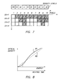
- Fig. 7 is a graph illustrating the conversion of a 10-resistor-head subjected to image data of bytes consisting of 2 bits.
- Fig. 8 is a curve relating the expected optical print density to the applied time modulation.
- a thermal dye transfer printer including a P/S conversion according to the present invention is schematically illustrated in Fig. 1 .
- a thermal dye transfer printing normally includes an image input 1 with interface 2, a line memory 3, several image corrections 4, a storage unit 5, a color selection switch 6, a RAM memory 7, a P/S conversion 8 , a latch and strobe circuit 9 & 10, output drivers 11, printing head 12, printing head corrections, clock synchronisation signals etc.
- the data stored in the storage unit 5 are read per separate color using a switch selector 6.
- the serial data 21 thus created are delivered to a shift register, which is p bits wide, for sequentially shifting one line of serially received picture data on the basis of a clock 23 and for outputting the stored one line picture data in a geometrically parallel manner as illustrated.
- the heat-sensitive head includes a shift register supplied with serial heating data 21 from the P/S converter and producing parallel data to a latch circuit 24 for holding these data from the shift register over a 1-line-level printing period, and an AND circuit 26 connected for each bit of the latch circuit and applying to the heat-generating resistor 28 an output from the latch circuit.
- pixel data are temporarily stored by a LATCH-circuit 24 which receives and latches input trains of data representing the gradations of the image elements of the original document. Indeed, after the p bits representing a print-line have been entered in the (head-driver) shift register 22, a Latch signal 25 is supplied to activate p latches 24 so that all p bits from the shift register 22 are transferred in parrallel to the latches 24. From now on, these pixel data then are available to the appropriate logical gates, e. g. AND-elements 26. When the strobe signal 27 is given to these gates, the pixel data are delivered to the respective heat generating elements 28.
- a LATCH-circuit 24 receives and latches input trains of data representing the gradations of the image elements of the original document. Indeed, after the p bits representing a print-line have been entered in the (head-driver) shift register 22, a Latch signal 25 is supplied to activate p latches 24 so that all p bits from the shift register
- Fig. 3 illustrates a prior art P/S conversion using a comparator as described in the European patent EP-B-0 208 919.
- the actual image data 31 e.g. bytes consisting of 8 bits in parallel
- the comparator 34 To the second input terminal 35 of the same comparator 34 is fed the sequentially incremented output of a clocked counter 36, making it possible to compare both byte-levels.
- a host computer 41 provides input variable image data corresponding to one image line or eventual one line part. This data are stored in parallel in a buffered line memory designated MEM 43 and are in the form of bytes, indicated symbolically as A data 44, each byte consisting, for example, of eight parallel bits A0 - A7, indicated symbolically as Ai.
- d image density gradiations
- MEM 43 is assumed to be of the FIFO (i.e. a "first-in, first-out") type but the experienced designer might occasionally employ an addressed type, i.e. RAM, for MEM 43.
- controller 46 of Fig. 4 controls, in clock synchronization, the writing in and reading ouf of image data to and from MEM 43 in four sequential steps :
- controller 46 is driven by a crystal 45 and at a given clockpulse, controller 46 reads out from MEM 43 all of the A data corresponding to a given first image line and transfers this A data to downcounter and non-zero detector 47.
- the downcounter and non-zero detector performs two functions, of which the downcounting function will be explained first, with reference to Fig. 4. (A particular embodiment of non-zero detector will be explained later with special reference to Fig. 6).
- Controller 46 restarts the reading out from MEM 43 the recalculated (now reduced value) A-data bytes in turn, i.e. beginning with the byte for the first image pixel, then the next, and so on until the last byte for the final pixel p of the given image line.
- the A-bytes of recalculated value are transferred from MEM 43 again to the non-zero detector and downcounter 47 and the sequence is repeated for several cycles through the steps of non-zero detection, downcounting, outputting, recirculating, and so on.
- A-data to B-data per cycle amounts to one incremental unit (one digital rank or bit), so that one has to expect a total of d number of cycles.
- Figs. 5a and 5b are separate flow charts illustrating the separate steps in the operation of the P/S conversion method of the present invention and will now be explained.
- the operational sequence can begin after the image data for one image line has been stored in the line memory in preparation for a recording operation.
- the correct access (input) status for MEM 43 must be chosen. This is done in a firste step S 1 by disabling #2 gate buffer 52, so that in the next step S 2, all of the A-date for the given line can be written into MEM 43 via #2 gate buffer.
- step S 3 MEM 43 is checked to determine if it is fully loaded (i.e. whether all of the image data for the given line has been loaded successfully into the memory). (This presupposes that MEM 43 is designed with a capacity for exactly p number of pixel bytes).
- step S 4 the input to MEM 43 is disabled at # 2 gate buffer 52 and enabled at # 1 gate buffer 50. This prevents further external access to MEM 43 but opens the possibility of writing in recirculated data.
- step S 5 all of the A-data are read out from MEM 43 to the downcounter and non-zero detector and in step S 6 such data are identified (verified) as to whether they are zero or non-zero.
- step S 11 writes the B-data into MEM 43 via the #1 gate buffer 50.
- image data for the next image line are accepted from the host computer into MEM 43, by repeating the same sequence of operation steps.
- Fig. 5b shows another embodiment of operational sequence, differing in that the one step S 12 is replaced by two steps S 13 and S 14.
- a method according to Fig. 5a ends as all non-zero levels have been reduced to zero.
- a method according to Fig. 5b ends as a maximum level G max, corresponding to a maximum density gradation variation in the original image or corresponding to a preset level, has been transferred and downcounted.
- G max corresponding to a maximum density gradation variation in the original image or corresponding to a preset level
- the reduced B byte data read out of the downcounter is not zero, signifying that at least one bit of a B byte is a logic one
- a signal C equal to a logic one bit is outputted from the downcounter to the shift register and thence to the latching memory circuit when the latter is activated.
- Enablement (strobing) of the latching memory circuit results in the application of a signal to the corresponding heating element of the thermal printing head for exactly one time unit which in turn results in the transfer to the receiving sheet of "one unit" of dye, equal to one density gradation level (one density step) of the image pixels. (The transfer of additional "units" of dye for the same pixel will be explained in connection with Fig. 7).
- each image byte has eight bits, as mentioned above, there is a possibility, as already noted, of 256 density gradation steps or levels.
- the existence of eight bit data per byte allows a total of 256 time units per heating element.
- the reading/recalculating/non zero detecting cycle would be repeated exactly d number of times.
- the printing of the initial line is terminated and the image data for the next line is applied to the line memory in preparation for printing of the next line.
- step S6 the operation of a non-zero detection circuit, constituted of simple OR-gates 61, 62, and 63, as seen in Fig. 6.
- a non-zero detection circuit constituted of simple OR-gates 61, 62, and 63, as seen in Fig. 6.
- the gate for a given pixel is read as zero, signifying that all of the bits Ai of the corresponding byte of image data are at logic zero, then a C-bit 48 equal to logic zero is outputted to the corresponding driving components of the thermal printing head which precludes any transfer of dye by the corresponding heating element.
- Fig. 6 which shows a non-zero detector for bytes each having eight bits and which uses OR-gates
- a downcounter could be built of discrete components as well as with gate array logics (e.g. gal, pal). Alternatively, the downcounter could be based on commercial components with integrated zero-detector. Further, if appropriate controls were provided, a different format for the data bytes (8, 10 or 12 bits per byte) would be handled.
- the thermal printing head normally includes a plurality of heating elements equal in number to the number of pixels in the image data present in the line memory.
- each of these heating elements is capable of being energized individually by heating pulses and that the number of heating pulses for each heating element is controlled in accordance with the density gradation level of the corresponding pixel
- Fig. 7 illustrates the heating pulse pattern for a ten element head for the simplified case where the number of pixels p equals ten and each pixel is represented by a signal byte having two bits (corresponding to a range of four density gradation levels or steps).
- zero density is represent by a bit logic of zero/zero, the first density step by a bit logic of zero/one, the second density step by a bit logic of one/zero, and the final density step by a bit logic of one/one.
- the overall pulse duration (width) - resulting from the integration of the number of individual pulses for a given heating element - will determine the total heating (recording) energy for a given heating element in a given image line.
- the heating time of the corresponding heating element will increase proportionally, thereby increasing the heat energy outputted by that element and thus increasing the heat energy outputted by that element and thus increasing the optical density of the dye transferred to the receiving sheet for that pixel. Contrarywise, where an image pixel data has a lower density level, the heating time is shortened and the corresponding "picture data" on the receiving sheet is lighter in density.
- Fig. 8 This relationship is shown graphically in Fig. 8 wherein a natural/normal density curve for a typical image is represented by the solid line 81 and a linear approximation of that curve is represented by a broken line 82.
- the exemplary P/S conversion circuit shown in Fig. 4 included only a single memory MEM and a single downcounter and non-zero detector, the capacity of the circuit for more density levels could easily be extended (by connecting more MEM's in parallel) or for more information per line (by connecting more MEM's in series).
- the image data could be stored entirely in the host computer and transferred line-by-line in sequence to the MEM, as was taken to be the case in the example described above, or they could be shifted to an addressed MEM with a capacity large enough for all the line data of a given color of a given image.
- the present invention can be applied to any type of thermal recording, including the type in which image data are thermally recorded directly on a thermal recording paper, and the type in which data are thermally transferred onto ordinary paper.
- the printing is not limited to the above-explained method employing a thermal head, but can also be applied by other technologies as resistive ribbon printing, dye diffusion resistor ribbon, ink-jet printing.
- the recording medium is not limited to a recording paper, but might be a textile or a plastic or a transparant for overhead projection.
Landscapes
- Engineering & Computer Science (AREA)
- Theoretical Computer Science (AREA)
- Multimedia (AREA)
- Signal Processing (AREA)
- Electronic Switches (AREA)
- Record Information Processing For Printing (AREA)
Claims (8)
- Procédé de réalisation d'une conversion électronique d'un train de signaux de données configurés parallèlement (42), chaque signal de données configuré parallèlement correspondant à un niveau de signal d'image d'un pixel d'une ligne d'une image d'origine à reproduire et variant en valeurs sur une gamme de niveaux, chaque niveau différant d'un niveau adjacent par une unité, de zéro à un maximum et correspondant à des variations de gradation de densité dans lesdits pixels de ladite image d'origine, en une configuration série de signaux (21) ayant un niveau unique au-dessus de zéro pour commander la reproduction de l'image d'origine en fournissant ledit train de signaux de données configurés parallèlement pixel par pixel dans une mémoire de lignes (43) ayant une capacité égale auxdits pixels de ladite au moins une ligne, le procédé étant caractérisé en ce qu'il comprend en outre, dans le cadre d'une synchronisation contrôlée, les étapes de:a. Transfert desdits signaux de données configurés parallèlement depuis la mémoire de lignes un à un vers un détecteur de valeur non nulle et décompteur (47) en vue d'une discrimination entre un niveau nul et un niveau non nul et d'une réduction de tous les niveaux non nuls ainsi discriminés par un niveau d'une unité tandis que les signaux de niveau nul restent à zéro,b. Production à partir dudit détecteur et décompteur (47) vers une mémoire de commande d'un train de signaux de commande (48) d'une valeur nulle pour tous les signaux de données discriminés comme étant nuls et d'une valeur d'unité pour tous les signaux de données discriminés comme non nuls tout en remplaçant les signaux de données présents dans la mémoire de lignes (43) par renvoi dans la mémoire de lignes du train de signaux de données aux signaux ayant tous un niveau non nul au niveau réduit, etc. Répétition des étapes a.-b. jusqu'à ce que tous les signaux de niveau non nul aient été réduits à zéro.
- Procédé conformément à la revendication 1, dans lequel ladite mémoire de ligne (43) est une mémoire premier entré, premier sorti FIFO ou une mémoire vive RAM.
- Procédé conformément à la revendication 1, dans lequel ladite mémoire de commande comprend un registre à décalage (20) et un circuit de mémoire de verrouillage associé (24) qui sont adaptés en vue d'être actionnés pour recevoir et stocker les signaux de commande en séquence et fournir les signaux de commande.
- Procédé conformément à la revendication 3, dans lequel ledit original doit être reproduit au moyen d'une imprimante thermique qui comporte un certain nombre d'éléments d'impression (28) actionnables pour générer une reproduction et lesdits signaux de commande sont appliqués par ledit circuit de mémoire de verrouillage (24) sur ledit signal auxdits éléments d'impression pour actionner ceux-ci.
- Procédé conformément à la revendication 1 ou 4, dans lequel chacun desdits signaux de données électriques configurés parallèlement correspondant à un pixel d'une ligne d'une image d'origine, est égal en valeur à un niveau de gradation de densité d'une pluralité de pixels d'image d'une image d'origine sur une gamme de niveaux de gradation de densité allant de zéro à un maximum pour commander la reproduction de l'image d'origine sur un moyen récepteur dans une imprimante thermique ayant des éléments d'impression contrôlables correspondant en nombre aux pixels dans une ligne d'image et un circuit d'actionnement pour actionner les éléments d'impression respectifs de manière accessible individuellement.
- Procédé conformément à la revendication 5, dans lequel l'étape c est remplacée par les étapes de:c. Actionnement des éléments d'impression de ladite imprimante thermique par le circuit d'actionnement en correspondance avec lesdits signaux de commande ayant chacun une durée d'une unité de temps qui est sélectionnée pour être égale à une reproduction par ladite imprimante thermique sur ledit moyen récepteur d'une image ayant un niveau de gradation de densité,d. Ledit renvoi comprenant le remplacement des signaux électriques dans ladite mémoire de lignes en renvoyant à l'entrée de ladite mémoire de lignes les signaux de valeur nulle et les signaux de valeur réduite non nulle provenant du détecteur et décompteur pour le transfert une nouvelle fois audit détecteur de valeur non nulle et décompteur, ete. Répétition des étapes a. à d. pour un nombre total de cycles nécessaire pour que toutes les valeurs de signaux non nulles soient réduites à zéro, de telle sorte que les éléments d'impression de ladite imprimante soient actionnés pendant un certain nombre de périodes de temps égal au nombre total de cycles pour reproduire sur ladite feuille réceptrice les images desdits pixels de ladite ligne d'image d'origine variant en densité en correspondance avec les variations de densité des pixels de ladite image d'origine.
- Procédé de la revendication 6, dans lequel ledit train de signaux électriques représente une ligne unique d'un pixel d'une seule couleur dérivée d'un original multicolore.
- Procédé de la revendication 7, dans lequel ledit original multicolore contient les couleurs magenta, cyan et jaune, et facultativement noire, et les pixels représentés par lesdits signaux sont de l'une desdites couleurs.
Priority Applications (4)
| Application Number | Priority Date | Filing Date | Title |
|---|---|---|---|
| EP91201608A EP0520093B1 (fr) | 1991-06-24 | 1991-06-24 | Conversion parallèle-série de données d'information |
| DE69122382T DE69122382T2 (de) | 1991-06-24 | 1991-06-24 | Parallel-Serie-Umwandlung von Informationsdaten |
| US07/895,837 US5440684A (en) | 1991-06-24 | 1992-06-09 | Parallel to serial conversion of information data |
| JP18862792A JPH05298040A (ja) | 1991-06-24 | 1992-06-22 | 情報データの並列構成から直列構成への変換方法 |
Applications Claiming Priority (1)
| Application Number | Priority Date | Filing Date | Title |
|---|---|---|---|
| EP91201608A EP0520093B1 (fr) | 1991-06-24 | 1991-06-24 | Conversion parallèle-série de données d'information |
Publications (2)
| Publication Number | Publication Date |
|---|---|
| EP0520093A1 EP0520093A1 (fr) | 1992-12-30 |
| EP0520093B1 true EP0520093B1 (fr) | 1996-09-25 |
Family
ID=8207736
Family Applications (1)
| Application Number | Title | Priority Date | Filing Date |
|---|---|---|---|
| EP91201608A Expired - Lifetime EP0520093B1 (fr) | 1991-06-24 | 1991-06-24 | Conversion parallèle-série de données d'information |
Country Status (4)
| Country | Link |
|---|---|
| US (1) | US5440684A (fr) |
| EP (1) | EP0520093B1 (fr) |
| JP (1) | JPH05298040A (fr) |
| DE (1) | DE69122382T2 (fr) |
Families Citing this family (5)
| Publication number | Priority date | Publication date | Assignee | Title |
|---|---|---|---|---|
| US5786837A (en) | 1994-11-29 | 1998-07-28 | Agfa-Gevaert N.V. | Method and apparatus for thermal printing with voltage-drop compensation |
| JPH0939306A (ja) * | 1995-07-28 | 1997-02-10 | Brother Ind Ltd | 印字装置 |
| US6147699A (en) * | 1998-11-10 | 2000-11-14 | Lexmark International, Inc. | Low electromagnetic emissions and improved signal quality video drive architecture for laser printers |
| JP2001010113A (ja) * | 1999-04-27 | 2001-01-16 | Mitsubishi Electric Corp | 光プリント装置 |
| US7342977B2 (en) * | 2002-11-26 | 2008-03-11 | Lsi Logic Corporation | Serial data transmitter with bit doubling |
Family Cites Families (7)
| Publication number | Priority date | Publication date | Assignee | Title |
|---|---|---|---|---|
| US4513313A (en) * | 1982-12-07 | 1985-04-23 | Canon Kabushiki Kaisha | Solid state imaging device |
| US4731673A (en) * | 1984-03-22 | 1988-03-15 | Canon Kabushiki Kaisha | Image output device |
| DE3688715D1 (de) * | 1985-03-30 | 1993-08-26 | Hitachi Ltd | Druckverfahren vom abtastaufzeichnungstyp und dessen verwirklichungsvorrichtung. |
| US5300960A (en) * | 1988-12-27 | 1994-04-05 | Eastman Kodak Company | Dot printer and method for grey level recording and circuit for use in same |
| EP0760578B1 (fr) * | 1989-10-02 | 2003-04-02 | Canon Kabushiki Kaisha | Dispositif pour la formation d'image et procédé de modulation |
| US5111217A (en) * | 1989-12-18 | 1992-05-05 | Eastman Kodak Company | Dot printer and method for grey level recording |
| US5200765A (en) * | 1990-03-26 | 1993-04-06 | Eastman Kodak Company | Apparatus and method for calibrating a grey level printhead |
-
1991
- 1991-06-24 DE DE69122382T patent/DE69122382T2/de not_active Expired - Fee Related
- 1991-06-24 EP EP91201608A patent/EP0520093B1/fr not_active Expired - Lifetime
-
1992
- 1992-06-09 US US07/895,837 patent/US5440684A/en not_active Expired - Fee Related
- 1992-06-22 JP JP18862792A patent/JPH05298040A/ja active Pending
Also Published As
| Publication number | Publication date |
|---|---|
| DE69122382D1 (de) | 1996-10-31 |
| US5440684A (en) | 1995-08-08 |
| EP0520093A1 (fr) | 1992-12-30 |
| DE69122382T2 (de) | 1997-04-03 |
| JPH05298040A (ja) | 1993-11-12 |
Similar Documents
| Publication | Publication Date | Title |
|---|---|---|
| US4540991A (en) | Thermal printing system | |
| JPS6036397B2 (ja) | 熱記録装置 | |
| US4563693A (en) | Gradation recorder | |
| EP0520093B1 (fr) | Conversion parallèle-série de données d'information | |
| JP2896249B2 (ja) | プリンタの記録ヘッド駆動装置 | |
| JPH0632942B2 (ja) | 記録濃度制御装置 | |
| US5382965A (en) | Wax transfer type thermal printing method and thermal printer | |
| US5363125A (en) | Method and device for correcting shading in thermal printer | |
| EP0215471A2 (fr) | Appareil d'enregistrement thermique | |
| US4894712A (en) | Density gradation control type thermal printer | |
| JPS6115469A (ja) | サ−マル記録装置 | |
| US5734410A (en) | Thermal transfer recording apparatus and method for regularly assigning blank dots | |
| US5347597A (en) | Image scaling for thermal printers and the like | |
| JPH0370633B2 (fr) | ||
| JPS6345069A (ja) | 感熱記録装置 | |
| JPS61172479A (ja) | 感熱記録装置 | |
| JP3017881B2 (ja) | サーマルプリンタ | |
| JPS61194975A (ja) | 中間調記録方法 | |
| JPH0236958A (ja) | 多階調熱記録における通電制御方法 | |
| JPS62284574A (ja) | 画像記録装置 | |
| JPS6313390B2 (fr) | ||
| JP2638041B2 (ja) | プリンタ装置 | |
| JPH0538837A (ja) | サーマルヘツド駆動装置 | |
| JPH07156433A (ja) | 熱転写プリンタの制御方法 | |
| JPH10151806A (ja) | カラー画像記録方法、カラー画像記録装置、及びカラー画像記録制御方法 |
Legal Events
| Date | Code | Title | Description |
|---|---|---|---|
| PUAI | Public reference made under article 153(3) epc to a published international application that has entered the european phase |
Free format text: ORIGINAL CODE: 0009012 |
|
| AK | Designated contracting states |
Kind code of ref document: A1 Designated state(s): AT BE CH DE DK ES FR GB GR IT LI LU NL SE |
|
| 17P | Request for examination filed |
Effective date: 19930505 |
|
| 17Q | First examination report despatched |
Effective date: 19950310 |
|
| GRAG | Despatch of communication of intention to grant |
Free format text: ORIGINAL CODE: EPIDOS AGRA |
|
| GRAH | Despatch of communication of intention to grant a patent |
Free format text: ORIGINAL CODE: EPIDOS IGRA |
|
| GRAA | (expected) grant |
Free format text: ORIGINAL CODE: 0009210 |
|
| GRAH | Despatch of communication of intention to grant a patent |
Free format text: ORIGINAL CODE: EPIDOS IGRA |
|
| AK | Designated contracting states |
Kind code of ref document: B1 Designated state(s): BE DE FR GB |
|
| PG25 | Lapsed in a contracting state [announced via postgrant information from national office to epo] |
Ref country code: BE Effective date: 19960925 |
|
| REF | Corresponds to: |
Ref document number: 69122382 Country of ref document: DE Date of ref document: 19961031 |
|
| ET | Fr: translation filed | ||
| PLBE | No opposition filed within time limit |
Free format text: ORIGINAL CODE: 0009261 |
|
| STAA | Information on the status of an ep patent application or granted ep patent |
Free format text: STATUS: NO OPPOSITION FILED WITHIN TIME LIMIT |
|
| 26N | No opposition filed | ||
| PGFP | Annual fee paid to national office [announced via postgrant information from national office to epo] |
Ref country code: GB Payment date: 19980429 Year of fee payment: 8 |
|
| PGFP | Annual fee paid to national office [announced via postgrant information from national office to epo] |
Ref country code: FR Payment date: 19980504 Year of fee payment: 8 |
|
| REG | Reference to a national code |
Ref country code: GB Ref legal event code: 746 Effective date: 19980601 |
|
| REG | Reference to a national code |
Ref country code: FR Ref legal event code: D6 |
|
| PG25 | Lapsed in a contracting state [announced via postgrant information from national office to epo] |
Ref country code: GB Free format text: LAPSE BECAUSE OF NON-PAYMENT OF DUE FEES Effective date: 19990624 |
|
| PG25 | Lapsed in a contracting state [announced via postgrant information from national office to epo] |
Ref country code: FR Free format text: THE PATENT HAS BEEN ANNULLED BY A DECISION OF A NATIONAL AUTHORITY Effective date: 19990630 |
|
| GBPC | Gb: european patent ceased through non-payment of renewal fee |
Effective date: 19990624 |
|
| REG | Reference to a national code |
Ref country code: FR Ref legal event code: ST |
|
| PGFP | Annual fee paid to national office [announced via postgrant information from national office to epo] |
Ref country code: DE Payment date: 20070529 Year of fee payment: 17 |
|
| PG25 | Lapsed in a contracting state [announced via postgrant information from national office to epo] |
Ref country code: DE Free format text: LAPSE BECAUSE OF NON-PAYMENT OF DUE FEES Effective date: 20090101 |