EP0522461B1 - Dispositif semi-conducteur scellé du type "Flip chip" - Google Patents
Dispositif semi-conducteur scellé du type "Flip chip" Download PDFInfo
- Publication number
- EP0522461B1 EP0522461B1 EP92111291A EP92111291A EP0522461B1 EP 0522461 B1 EP0522461 B1 EP 0522461B1 EP 92111291 A EP92111291 A EP 92111291A EP 92111291 A EP92111291 A EP 92111291A EP 0522461 B1 EP0522461 B1 EP 0522461B1
- Authority
- EP
- European Patent Office
- Prior art keywords
- substrate
- semiconductor chip
- semiconductor device
- chip
- metallic pattern
- Prior art date
- Legal status (The legal status is an assumption and is not a legal conclusion. Google has not performed a legal analysis and makes no representation as to the accuracy of the status listed.)
- Expired - Lifetime
Links
Images

Classifications
-
- H—ELECTRICITY
- H10—SEMICONDUCTOR DEVICES; ELECTRIC SOLID-STATE DEVICES NOT OTHERWISE PROVIDED FOR
- H10W—GENERIC PACKAGES, INTERCONNECTIONS, CONNECTORS OR OTHER CONSTRUCTIONAL DETAILS OF DEVICES COVERED BY CLASS H10
- H10W76/00—Containers; Fillings or auxiliary members therefor; Seals
- H10W76/60—Seals
-
- H—ELECTRICITY
- H10—SEMICONDUCTOR DEVICES; ELECTRIC SOLID-STATE DEVICES NOT OTHERWISE PROVIDED FOR
- H10W—GENERIC PACKAGES, INTERCONNECTIONS, CONNECTORS OR OTHER CONSTRUCTIONAL DETAILS OF DEVICES COVERED BY CLASS H10
- H10W74/00—Encapsulations, e.g. protective coatings
- H10W74/10—Encapsulations, e.g. protective coatings characterised by their shape or disposition
- H10W74/111—Encapsulations, e.g. protective coatings characterised by their shape or disposition the semiconductor body being completely enclosed
-
- H—ELECTRICITY
- H10—SEMICONDUCTOR DEVICES; ELECTRIC SOLID-STATE DEVICES NOT OTHERWISE PROVIDED FOR
- H10W—GENERIC PACKAGES, INTERCONNECTIONS, CONNECTORS OR OTHER CONSTRUCTIONAL DETAILS OF DEVICES COVERED BY CLASS H10
- H10W72/00—Interconnections or connectors in packages
- H10W72/071—Connecting or disconnecting
- H10W72/072—Connecting or disconnecting of bump connectors
- H10W72/07231—Techniques
- H10W72/07236—Soldering or alloying
-
- H—ELECTRICITY
- H10—SEMICONDUCTOR DEVICES; ELECTRIC SOLID-STATE DEVICES NOT OTHERWISE PROVIDED FOR
- H10W—GENERIC PACKAGES, INTERCONNECTIONS, CONNECTORS OR OTHER CONSTRUCTIONAL DETAILS OF DEVICES COVERED BY CLASS H10
- H10W74/00—Encapsulations, e.g. protective coatings
-
- H—ELECTRICITY
- H10—SEMICONDUCTOR DEVICES; ELECTRIC SOLID-STATE DEVICES NOT OTHERWISE PROVIDED FOR
- H10W—GENERIC PACKAGES, INTERCONNECTIONS, CONNECTORS OR OTHER CONSTRUCTIONAL DETAILS OF DEVICES COVERED BY CLASS H10
- H10W90/00—Package configurations
- H10W90/701—Package configurations characterised by the relative positions of pads or connectors relative to package parts
- H10W90/751—Package configurations characterised by the relative positions of pads or connectors relative to package parts of bond wires
- H10W90/756—Package configurations characterised by the relative positions of pads or connectors relative to package parts of bond wires between a chip and a stacked lead frame, conducting package substrate or heat sink
Definitions
- the present invention relates generally to a semiconductor device. More particularly, the present invention relates to an improved structure of a semiconductor device wherein a semiconductor chip is mounted on a substrate by employing a flip chip process, and thereafter, both of the semiconductor chip and the substrate are sealed with a synthetic resin while they are incorporated in the semiconductor device.
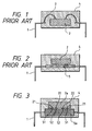
- Fig. 1 is a sectional view illustrating a typical structure of a semiconductor device of the conventional type. As shown in Fig. 1, the semiconductor device is constructed such that outer terminals 1 are connected to a semiconductor chip 2 via wires 3 bonded to them, and thereafter, an assembly of the outer terminals 1, the semiconductor chip 2 and the wires 3 is sealed with a synthetic resin 4.
- Fig. 2 is a sectional view illustrating the structure of another type of the conventional semiconductor device.
- the semiconductor device is constructed such that after a semiconductor chip 2 is once mounted on a substrate 5 by employing a flip chip process, an assembly of the semiconductor chip 2 and the substrate 5 is sealed with a synthetic resin 4 while they are incorporated in the semiconductor device. Outer terminals 1 are previously secured to the substrate 5. thus, in this case, no bonding wire is used for the semiconductor device.
- the flip chip process is disclosed, for example, in "LSI Assembly Technique", Silver Series No. 12, pages 63 to 82, issued on March 31, 1987.
- the synthetic resin 4 sealing the semiconductor chip 2 in the semiconductor device is used for the purpose of physically and chemically protecting the semiconductor chip 2.
- the properties of the semiconductor device are deteriorated as time passes.
- deterioration of the properties of the semiconductor device quickly proceed in a moist environment having an elevated temperature.
- Document JP-A-59 088 864 discloses a LSI device comprising a master substrate and a slave substrate, the main surface of which is smaller then that of the master substrate. Both substrates are placed in opposing relationship and are connected by solder bumps together with a solder dam surrounding the functional element parts so that those element parts are hermetically sealed. Laminated layers of Ti and Pt are used, to provide a pattern on each substrate, to which the solder is subsequently applied.
- an object of the invention is to provide an improved structure of a semiconductor device capable of improving durability that is, assuring that deterioration of the properties of the semiconductor device in the course of time can effectively be reduced.
- a semiconductor device including a substrate having terminals for electrical connection to the outside, a semiconductor chip mounted on the substrate by employing a flip chip process, and a synthetic resin for sealing the substrate and the semiconductor chip in the semiconductor device, wherein the semiconductor device includes a metallic pattern rectangularly formed on the functional surface of the semiconductor chip to completely surround the functional region on the semiconductor chip and a metallic pattern rectangularly formed on the substrate corresponding to the metallic pattern on the semiconductor chip, and that a gap between the semiconductor chip and the substrate is airtightly sealed with both the metallic patterns by connecting both the metallic pattern to each other when the semiconductor chip is mounted on the substrate.
- a feature of the semiconductor device of the present invention consists in that the metallic pattern is disposed on the surface of the semiconductor chip mounted on the base board so that the substrate and the semiconductor chip are airtightly connected to each other by utilizing the foregoing metallic pattern.
- shielding of the semiconductor chip from the surrounding environment is achieved merely in reliance on a sealing synthetic resin. Things are same in case that a flip chip process is employed for mounting the semiconductor chip on the substrate, and a gap between the semiconductor chip and the substrate is filled with a sealing synthetic resin.
- the sealing synthetic resin permits a small quantity of moisture or gas to practically permeate therethrough, integrated circuits and connection pads built on the surface of the semiconductor chip are unavoidably deteriorated due to the presence of moisture or the like in the environmental atmosphere.
- the semiconductor device of one embodiment of the present invention is constructed such that the metallic pattern rectangularly formed with a closed route-shaped contour is disposed on the functional surface of the semiconductor chip (coincident with the lower surface of the same when the semiconductor chip is mounted on the substrate by employing a flip chip process) in such a manner as to surround the functional region on the semiconductor chip.
- the rectangular metallic pattern is disposed on the surface of the substrate corresponding to the rectangular metallic pattern on the semiconductor chip.
- Fig. 3 is a sectional view of a semiconductor device in accordance with an embodiment of the present invention which illustrates by way of example the structure of the semiconductor device. It should be noted that same or similar parts or components to those shown in Fig. 2 are represented by same reference numerals.
- the semiconductor device is composed mainly of a substrate 5a, a semiconductor chip 2a mounted on the substrate 5a and a synthetic resin 4 with which an integral assembly of the substrate 5a and the semiconductor chip 2a is sealed in the semiconductor device.
- a rectangular extending metallic pattern 21 to be described later is formed on the mounting surface of the semiconductor chip 2a.
- a metallic pattern 51 is formed also on the mounting surface of the substrate 5a corresponding to the metallic pattern 21 of the semiconductor chip 2a.
- a gap between the semiconductor chip 2a and the substrate 5a is airtightly sealed by both the metallic patterns 21 and 51 on the semiconductor chip 2a and the substrate 5a.
- Outer terminals 1 are previously secured to the substrate 5a.
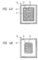
- Fig. 4 is a diagrammatical view which illustrates the functional surface of the semiconductor chip 2a in the semiconductor device shown in Fig. 3 in comparison with the semiconductor chip 2a used for conventional semiconductor device.
- the conventional semiconductor chip 2 includes a functional region 23 having integrated circuits and others, four pads 22, by way of which the functional region 23 is electrically connected to pads 52 on the substrate 5a, and a scribe line 24 for cutting the semiconductor chip 2 from a semiconductor wafer.
- the semiconductor chip 2a used for the semiconductor device of the present invention includes a functional region 23 having four pads 23 and a metallic pattern 21 rectangularly extending between the functional region 23 and a scribe line 24. As is apparent from the drawing, the functional region 23 is fully surrounded by the metallic pattern 21.
- Fig. 5 is a perspective view showing the structure of the substrate for mounting the semiconductor chip 2a constructed in the above-described manner in the disassembled state.
- pads 52 corresponding to the pads 22 on the semiconductor chip 2a and a rectangularly extending metallic pattern 51 corresponding to the metallic pattern 21 are formed on the base board 5a.
- the pads 52 are electrically connected to the pads 22 of the semiconductor chip 2a so that signals transmit therethrough between the semiconductor chip 2a and the substrate 5a.
- the pads 52 are electrically connected to the outer terminals 1 extending outside of the substrate 5a.
- the semiconductor chip 2a Since the semiconductor chip 2a is mounted on the substrate 5a constructed in the above-described manner while its functional region faces the functional surface of the substrate 5a, the structure as shown in Fig. 3 is built. For the purpose of physical or electrical protection of the semiconductor chip 2a and easy handling of the same, the whole assembly of the substrate 5a and the semiconductor chip 2a is sealed with a synthetic resin 4 in the semiconductor device.
- the functional region of the semiconductor chip 2a is completely sealably surrounded by a semiconductor wafer constituting the semiconductor chip 2a, the substrate 5a and the metallic patterns 21 and 51, there is no possibility that the functional region 23 on the semiconductor chip 2a is deteriorated in the presence of steam or the like.
- Fig. 6 is an enlarged sectional view showing a structure of the metallic patterns 21 and 51 along with a bonding connection therebetween.
- the metallic pattern 21 of the semiconductor chip 2a is formed by three-layers consisting of a first layer 21A formed of Ti, second layer 21B formed of Pt and third layer 21C formed of Au.
- the metallic pattern 51 of the substrate 51 is formed by three-layers consisting of a first layer 51A formed of Ti, second layer 51B formed of Pd and third layer 51C formed of Au.
- the third layer 21C of the semiconductor chip 2a faces the third layer 51 of the substrate 5a and bonded by adhesion 205 formed of AuSn containing 80% of Au and 20% of Sn.
- the metallic patterns 21, 51 thus formed are the best mode for a practical use because of a good durability and adhesibility. However, the invention is not limited thereto or thereby.
- the other material for each layer may be applicable if appropriate.
- the semiconductor device is constructed such that a gap between the substrate and the semiconductor chip mounted on the substrate by employing a flip chip process is completely sealed by the metallic pattern formed on the substrate and the metallic pattern formed on the semiconductor chip, there is no possibility that the functional region on the semiconductor chip is deteriorated due to the presence of moisture or gas permeated through the sealing synthetic resin. Consequently, the semiconductor device has a long running life, and moreover, it can practically be used under a very severe environmental condition such as a moist working environment having an elevated temperature.
Landscapes
- Wire Bonding (AREA)
- Structures Or Materials For Encapsulating Or Coating Semiconductor Devices Or Solid State Devices (AREA)
- Die Bonding (AREA)
Claims (3)
- Dispositif semi-conducteur comprenantun substrat (5a) comprenant :au moins une borne externe (1) s'étendant à l'extérieur du dispositif semi-conducteur ;au moins une plage (52) formée sur une surface dudit substrat (5a) pour raccorder électriquement ladite borne externe ; etun premier motif métallique (51) pour entourer ladite au moins une plage, et une puce semi-conductrice (2a) montée sur ledit substrat (5a) au moyen d'un procédé flip chip, ladite puce semi-conductrice comprenant :une zone fonctionnelle (23) en regard dudit substrat ;au moins une plage (22) placée sur une position sur ladite puce correspondant à ladite plage (52) dudit substrat pour que les signaux soit transmis à travers lesdites plages (22, 52) entre ladite puce semi-conductrice (2a) et ledit substrat (5a) lorsque ladite puce est montée sur ledit substrat ; etun second motif métallique (21) pour entourer ladite plage, ledit second motif métallique (21) étant raccordé complètement et de façon étanche à l'air audit premier motif métallique (51) dudit substrat pour enfermer et sceller hermétiquement la zone fonctionnelle (23) de ladite puce (2a) ;dans lequel ledit premier motif métallique (51) comprend une première couche de substrat (51A) formée de Ti et raccordée à ladite surface dudit substrat (5a),ledit second motif métallique (21) comprend une première couche de puce (21A) formée de Ti et raccordée à ladite surface de ladite puce semi-conductrice (2a) et une seconde couche de puce (21B) formée de Pt, etune couche adhésive (205) relie lesdits premier et second motifs métalliques,caractérisé en ce queledit premier motif métallique (51) comprend de plus une seconde couche de substrat (51B) formée de Pd et une troisième couche de substrat (51C) formée de Au,ledit second motif métallique (21) comprend de plus une troisième couche de puce (21C) formée de Au et en regard de cette troisième couche de substrat (51C), etladite couche adhésive (205) est formée de AuSn.
- Dispositif semi-conducteur selon la revendication 1, dans lequel ledit substrat (5a) et ladite puce semi-conductrice (2a) sont enrobés par une résine synthétique (4).
- Dispositif semi-conducteur selon la revendication 1, dans lequel ledit alliage AuSn de soudure (205) contient 80% de Au et 20% de Sn.
Applications Claiming Priority (2)
| Application Number | Priority Date | Filing Date | Title |
|---|---|---|---|
| JP195818/91 | 1991-07-10 | ||
| JP3195818A JPH0521654A (ja) | 1991-07-10 | 1991-07-10 | 半導体デバイス |
Publications (2)
| Publication Number | Publication Date |
|---|---|
| EP0522461A1 EP0522461A1 (fr) | 1993-01-13 |
| EP0522461B1 true EP0522461B1 (fr) | 1996-03-27 |
Family
ID=16347508
Family Applications (1)
| Application Number | Title | Priority Date | Filing Date |
|---|---|---|---|
| EP92111291A Expired - Lifetime EP0522461B1 (fr) | 1991-07-10 | 1992-07-03 | Dispositif semi-conducteur scellé du type "Flip chip" |
Country Status (6)
| Country | Link |
|---|---|
| EP (1) | EP0522461B1 (fr) |
| JP (1) | JPH0521654A (fr) |
| KR (1) | KR950014118B1 (fr) |
| AU (1) | AU653610B2 (fr) |
| CA (1) | CA2072734A1 (fr) |
| DE (1) | DE69209387T2 (fr) |
Families Citing this family (3)
| Publication number | Priority date | Publication date | Assignee | Title |
|---|---|---|---|---|
| FR2705832B1 (fr) * | 1993-05-28 | 1995-06-30 | Commissariat Energie Atomique | Procédé de réalisation d'un cordon d'étanchéité et de tenue mécanique entre un substrat et une puce hybridée par billes sur le substrat. |
| US5578874A (en) * | 1994-06-14 | 1996-11-26 | Hughes Aircraft Company | Hermetically self-sealing flip chip |
| KR100241592B1 (ko) * | 1998-10-28 | 2000-02-01 | 박대인 | 세라믹소재 보차도용 조립식 블록의 제조방법 |
Family Cites Families (3)
| Publication number | Priority date | Publication date | Assignee | Title |
|---|---|---|---|---|
| US3591839A (en) * | 1969-08-27 | 1971-07-06 | Siliconix Inc | Micro-electronic circuit with novel hermetic sealing structure and method of manufacture |
| JPS5988864A (ja) * | 1982-11-12 | 1984-05-22 | Matsushita Electric Ind Co Ltd | 半導体装置の製造方法 |
| JPH01238148A (ja) * | 1988-03-18 | 1989-09-22 | Fuji Electric Co Ltd | 半導体装置 |
-
1991
- 1991-07-10 JP JP3195818A patent/JPH0521654A/ja not_active Withdrawn
-
1992
- 1992-06-29 CA CA002072734A patent/CA2072734A1/fr not_active Abandoned
- 1992-07-03 DE DE69209387T patent/DE69209387T2/de not_active Expired - Fee Related
- 1992-07-03 EP EP92111291A patent/EP0522461B1/fr not_active Expired - Lifetime
- 1992-07-09 KR KR1019920012199A patent/KR950014118B1/ko not_active Expired - Fee Related
- 1992-07-09 AU AU19572/92A patent/AU653610B2/en not_active Ceased
Also Published As
| Publication number | Publication date |
|---|---|
| CA2072734A1 (fr) | 1993-01-11 |
| JPH0521654A (ja) | 1993-01-29 |
| KR950014118B1 (ko) | 1995-11-21 |
| AU653610B2 (en) | 1994-10-06 |
| DE69209387D1 (de) | 1996-05-02 |
| AU1957292A (en) | 1993-01-14 |
| EP0522461A1 (fr) | 1993-01-13 |
| DE69209387T2 (de) | 1996-08-29 |
| KR930003333A (ko) | 1993-02-24 |
Similar Documents
| Publication | Publication Date | Title |
|---|---|---|
| KR960003768B1 (ko) | 스택된 칩 어셈블리 및 그 제조방법 | |
| US6175149B1 (en) | Mounting multiple semiconductor dies in a package | |
| US5637828A (en) | High density semiconductor package | |
| US4661837A (en) | Resin-sealed radiation shield for a semiconductor device | |
| EP0331245B1 (fr) | Conteneur de puces à circuit intégré et procédé de fabrication | |
| GB2057757A (en) | Moulded lead frame dual in-line package and fabrication method therefor | |
| JPS63128736A (ja) | 半導体素子 | |
| US5168345A (en) | Semiconductor device having a universal die size inner lead layout | |
| EP0710982A2 (fr) | Zone personnalisé d'un cadre de conducteur estampé ou semi-gravé pour réduire les contraintes mécaniques sur les bords d'une puce | |
| KR100391094B1 (ko) | 듀얼 다이 패키지와 그 제조 방법 | |
| US5349233A (en) | Lead frame and semiconductor module using the same having first and second islands and three distinct pluralities of leads and semiconductor module using the lead frame | |
| EP0522461B1 (fr) | Dispositif semi-conducteur scellé du type "Flip chip" | |
| KR100825784B1 (ko) | 휨 및 와이어 단선을 억제하는 반도체 패키지 및 그제조방법 | |
| KR100207902B1 (ko) | 리드 프레임을 이용한 멀티 칩 패키지 | |
| KR20000040586A (ko) | 회로배선이 형성된 기판을 갖는 멀티 칩 패키지 | |
| KR100431182B1 (ko) | 표면 탄성파 필터 칩 패키지 및 그 제조방법 | |
| JPH0382059A (ja) | 樹脂封止型半導体装置 | |
| JPH06216306A (ja) | 半導体素子アセンブリ用内部キャパシタ配設構造およびその配設方法 | |
| JPH0536861A (ja) | 半導体デバイス | |
| KR100279252B1 (ko) | 세라믹패키지 | |
| JP2633557B2 (ja) | 樹脂封止型集積回路装置 | |
| KR20000040218A (ko) | 멀티 칩 패키지 | |
| KR0138301B1 (ko) | 리드 온 칩(loc) 구조의 패키지 | |
| KR200147420Y1 (ko) | 멀티 칩 모듈 반도체 장치 | |
| KR100468024B1 (ko) | Loc패키지 |
Legal Events
| Date | Code | Title | Description |
|---|---|---|---|
| PUAI | Public reference made under article 153(3) epc to a published international application that has entered the european phase |
Free format text: ORIGINAL CODE: 0009012 |
|
| AK | Designated contracting states |
Kind code of ref document: A1 Designated state(s): CH DE FR GB IT LI NL |
|
| 17P | Request for examination filed |
Effective date: 19930226 |
|
| 17Q | First examination report despatched |
Effective date: 19940613 |
|
| GRAH | Despatch of communication of intention to grant a patent |
Free format text: ORIGINAL CODE: EPIDOS IGRA |
|
| GRAA | (expected) grant |
Free format text: ORIGINAL CODE: 0009210 |
|
| AK | Designated contracting states |
Kind code of ref document: B1 Designated state(s): CH DE FR GB IT LI NL |
|
| PG25 | Lapsed in a contracting state [announced via postgrant information from national office to epo] |
Ref country code: IT Free format text: LAPSE BECAUSE OF FAILURE TO SUBMIT A TRANSLATION OF THE DESCRIPTION OR TO PAY THE FEE WITHIN THE PRE;WARNING: LAPSES OF ITALIAN PATENTS WITH EFFECTIVE DATE BEFORE 2007 MAY HAVE OCCURRED AT ANY TIME BEFORE 2007. THE CORRECT EFFECTIVE DATE MAY BE DIFFERENT FROM THE ONE RECORDED.SCRIBED TIME-LIMIT Effective date: 19960327 Ref country code: CH Effective date: 19960327 Ref country code: FR Effective date: 19960327 Ref country code: NL Free format text: LAPSE BECAUSE OF FAILURE TO SUBMIT A TRANSLATION OF THE DESCRIPTION OR TO PAY THE FEE WITHIN THE PRESCRIBED TIME-LIMIT Effective date: 19960327 Ref country code: LI Effective date: 19960327 |
|
| REF | Corresponds to: |
Ref document number: 69209387 Country of ref document: DE Date of ref document: 19960502 |
|
| PG25 | Lapsed in a contracting state [announced via postgrant information from national office to epo] |
Ref country code: GB Effective date: 19960703 |
|
| EN | Fr: translation not filed | ||
| NLV1 | Nl: lapsed or annulled due to failure to fulfill the requirements of art. 29p and 29m of the patents act | ||
| REG | Reference to a national code |
Ref country code: CH Ref legal event code: PL |
|
| PLBE | No opposition filed within time limit |
Free format text: ORIGINAL CODE: 0009261 |
|
| STAA | Information on the status of an ep patent application or granted ep patent |
Free format text: STATUS: NO OPPOSITION FILED WITHIN TIME LIMIT |
|
| GBPC | Gb: european patent ceased through non-payment of renewal fee |
Effective date: 19960703 |
|
| 26N | No opposition filed | ||
| PG25 | Lapsed in a contracting state [announced via postgrant information from national office to epo] |
Ref country code: DE Effective date: 19970402 |