EP0534406A1 - Mechanismus zum parallelen Halten einer Fläche und Apparat zur Verwendung eines solchen Mechanismus - Google Patents
Mechanismus zum parallelen Halten einer Fläche und Apparat zur Verwendung eines solchen Mechanismus Download PDFInfo
- Publication number
- EP0534406A1 EP0534406A1 EP92116287A EP92116287A EP0534406A1 EP 0534406 A1 EP0534406 A1 EP 0534406A1 EP 92116287 A EP92116287 A EP 92116287A EP 92116287 A EP92116287 A EP 92116287A EP 0534406 A1 EP0534406 A1 EP 0534406A1
- Authority
- EP
- European Patent Office
- Prior art keywords
- base plate
- weight
- parallel plane
- holding mechanism
- electrodes
- Prior art date
- Legal status (The legal status is an assumption and is not a legal conclusion. Google has not performed a legal analysis and makes no representation as to the accuracy of the status listed.)
- Granted
Links
Images


Classifications
-
- G—PHYSICS
- G01—MEASURING; TESTING
- G01Q—SCANNING-PROBE TECHNIQUES OR APPARATUS; APPLICATIONS OF SCANNING-PROBE TECHNIQUES, e.g. SCANNING PROBE MICROSCOPY [SPM]
- G01Q10/00—Scanning or positioning arrangements, i.e. arrangements for actively controlling the movement or position of the probe
- G01Q10/04—Fine scanning or positioning
-
- B—PERFORMING OPERATIONS; TRANSPORTING
- B82—NANOTECHNOLOGY
- B82Y—SPECIFIC USES OR APPLICATIONS OF NANOSTRUCTURES; MEASUREMENT OR ANALYSIS OF NANOSTRUCTURES; MANUFACTURE OR TREATMENT OF NANOSTRUCTURES
- B82Y35/00—Methods or apparatus for measurement or analysis of nanostructures
-
- G—PHYSICS
- G01—MEASURING; TESTING
- G01B—MEASURING LENGTH, THICKNESS OR SIMILAR LINEAR DIMENSIONS; MEASURING ANGLES; MEASURING AREAS; MEASURING IRREGULARITIES OF SURFACES OR CONTOURS
- G01B5/00—Measuring arrangements characterised by the use of mechanical techniques
- G01B5/0002—Arrangements for supporting, fixing or guiding the measuring instrument or the object to be measured
- G01B5/0004—Supports
-
- G—PHYSICS
- G11—INFORMATION STORAGE
- G11B—INFORMATION STORAGE BASED ON RELATIVE MOVEMENT BETWEEN RECORD CARRIER AND TRANSDUCER
- G11B9/00—Recording or reproducing using a method not covered by one of the main groups G11B3/00 - G11B7/00; Record carriers therefor
- G11B9/12—Recording or reproducing using a method not covered by one of the main groups G11B3/00 - G11B7/00; Record carriers therefor using near-field interactions; Record carriers therefor
- G11B9/14—Recording or reproducing using a method not covered by one of the main groups G11B3/00 - G11B7/00; Record carriers therefor using near-field interactions; Record carriers therefor using microscopic probe means, i.e. recording or reproducing by means directly associated with the tip of a microscopic electrical probe as used in Scanning Tunneling Microscopy [STM] or Atomic Force Microscopy [AFM] for inducing physical or electrical perturbations in a recording medium; Record carriers or media specially adapted for such transducing of information
-
- B—PERFORMING OPERATIONS; TRANSPORTING
- B82—NANOTECHNOLOGY
- B82Y—SPECIFIC USES OR APPLICATIONS OF NANOSTRUCTURES; MEASUREMENT OR ANALYSIS OF NANOSTRUCTURES; MANUFACTURE OR TREATMENT OF NANOSTRUCTURES
- B82Y10/00—Nanotechnology for information processing, storage or transmission, e.g. quantum computing or single electron logic
-
- Y—GENERAL TAGGING OF NEW TECHNOLOGICAL DEVELOPMENTS; GENERAL TAGGING OF CROSS-SECTIONAL TECHNOLOGIES SPANNING OVER SEVERAL SECTIONS OF THE IPC; TECHNICAL SUBJECTS COVERED BY FORMER USPC CROSS-REFERENCE ART COLLECTIONS [XRACs] AND DIGESTS
- Y10—TECHNICAL SUBJECTS COVERED BY FORMER USPC
- Y10S—TECHNICAL SUBJECTS COVERED BY FORMER USPC CROSS-REFERENCE ART COLLECTIONS [XRACs] AND DIGESTS
- Y10S977/00—Nanotechnology
- Y10S977/84—Manufacture, treatment, or detection of nanostructure
- Y10S977/849—Manufacture, treatment, or detection of nanostructure with scanning probe
- Y10S977/86—Scanning probe structure
- Y10S977/872—Positioner
Definitions
- the invention relates to a parallel plane holding mechanism which can arbitrarily hold a parallel state and an apparatus using such a mechanism.
- the distance between the probe and the measuring object or the recording medium is changed in dependence on the surface state of the measuring object or recording medium, it is necessary to perform a control such that the probe is allowed to approach in the direction perpendicular to the distance or the micro surface or the like.
- a manipulator which can perform a fine FF operation to a stage on which the recording medium has been put is used and, in order to incline the probe, a cylindrical type piezoelectric actuator (piezoelectric tube) is connected to the probe and controlled.
- Fig. 1 shows a parallel plane holding mechanism using the piezoelectric tube which has conventionally been used.
- a radius of tube 1 is set to 16.5 mm, a thickness is set to 1.5 mm, and a length is set to 20 mm.
- a plate-shaped member 2 connected to the piezoelectric tube 1 can be inclined by about 1.4 x 10 ⁇ 6 rad.
- a parallel plane holding mechanism comprising: a structure having beams made of elastic members in a peripheral portion of a flat plate-shaped weight; a base plate arranged so as to face the weight; and electrodes arranged in both opposite surfaces of the weight and the base plate, wherein by applying voltages to the electrodes, the distance between the weight and the base plate is controlled and the structure and/or an object to be driven which is connected to the base plate are/is moved, thereby keeping a reference surface of the object in parallel with a predetermined reference surface.
- the voltages are applied to the opposite electrodes and the distance between the flat plate-shaped weight and the base plate is controlled, thereby arbitrarily keeping the reference surface of the object in parallel with an external reference surface, and on the other hand, the object to be driven or the recording medium which is connected to the base plate is three-dimensionally moved, thereby adjusting the positional relation with a stylus and arbitrarily keeping the parallel state.
- Fig. 2 shows a cross sectional view of a fundamental structure of a parallel plane holding mechanism.
- a mechanism 11 has a structure in which a driver 12 and a base plate 13 are joined in a peripheral junction portion 14.
- the driver 12 comprises a supporting portion 15, a flat plate-shaped weight 16, and beams 17 made of elastic members.
- a flat plane-shaped electrode 18 is formed on a lower surface of the weight 16. Electrodes 19a and 19b are also formed on the base plate 13 so as to face the electrode 18.
- the driver 12 is mainly made of an Si monocrystalline material.
- the beam 17 as an elastic member is made of a material such as Si, SiO2, Si3N4, or the like.
- An object 20 to be held in parallel is attached on the flat plate-shaped weight 16.
- a distance and a positional relation between the object 20 and an object 21 locating at a spatially remote position can be arbitrarily controlled.
- the object 20 to be held in parallel may be also connected to the upper portion of the flat plate-shaped weight 16 as shown in Fig. 2 or may also have a structure such that it is constructed integratedly with the weight 16.
- the actuation of the mechanism 11 is controlled by a voltage applied to the electrode 18 attached to the lower portion of the weight 16 and by voltages applied to the fixed electrodes 19a and 19b on the base plate 13. For instance, by connecting the electrode 18 to the ground and by applying a voltage +V to the electrode 19a and a voltage -V to the electrode 19b, an electrostatic attracting force and a repulsive force are generated by charges which are induced in the electrode 18.
- the weight 16 moves so as to widen the gap over the electrode 19a and to narrow the gap over the electrode 19b.
- the driving portion 12 and the base plate 13 are adhered so that the gap lies within a range from 0.5 to 20 ⁇ m in a balance state in which no voltage is applied.
- the weight 16 moves from the position in the balance state due to the bending or extension of the beams 17.
- the object 20 put on the weight 16 can be moved and controlled to the position as shown in, for example, Fig. 2 from the position in the balance state which is parallel with the base plate 13.
- the flat plate-shaped weight 16 is supported to the peripheral supporting portion 15 through a plurality of beams 17 made of the elastic members and has the electrode 18 on the lower surface.
- the electrodes 19a and 19b are formed on the upper surface of the base plate 13 so as to face the electrode 18.
- the peripheral junction portion 14 of the base plate 13 is adhered to the supporting portion 15.
- the weight 16 is driven by the electrostatic forces of the voltages which are applied to the electrodes 18, 19a and 19b. Electrostatic capacitances among the electrodes 18, 19a, and 19b are detected and a feedback control is executed so that the upper surface of the object 20 attached to the weight 16 is parallel with the lower surface of the external object 21. In this manner, the inclinations of the objects 20 and 21 are corrected.
- the parallel plane holding mechanism of the invention comprises: the structure having the beams made of the elastic members in the peripheral portion of the flat plate-shaped weight; the base plate arranged so as to face the weight; and the electrodes arranged on both of the opposite surfaces of the weight and the base plate, wherein by applying the voltages to the electrodes, the distance between the weight and the base plate is controlled and the structure and/or the object to be driven which is connected to the base plate are/is moved, thereby keeping the reference surface of the object in parallel with a predetermined reference surface.
- the above feedback control is constructed in a manner such that voltages are applied to the electrodes arranged to the weight and the base plate and a change in impedance is caused due to a change in capacitance by a change in gap, a change in partial voltage of the voltage between the electrodes is extracted as a signal and is fed back, thereby allowing an electrostatic force to act on the electrodes so as not to deviate the weight and the base plate.
- the above feedback control can be also constructed in a manner such that a current is supplied to either one of coils which are formed from the electrodes arranged to the weight and the base plate, a change in impedance is caused due to a change in gap by the other one of the coils, a change incurrent between the electrodes is extracted as a signal and is fed back, thereby allowing an electromagnetic force to act on the electrodes so as not to deviate the weight and the base plate.
- the driving portion 12 uses an Si monocrystal as a raw material.
- a patterning mask of the portion to form the weight 16 is formed from the back surface of an Si wafer having front and back mirror surfaces by a desired pattern.
- An etching is executed by using an anisotropic etchant of Si such as KOH or the like in accordance with the patterning mask, thereby forming the driving portion 12 of a three-dimensional structure having the desired weight 16.
- a thickness of the portion of the beam 17 is controlled by using a concentration dependent etching.
- a mask is formed in a manner similar to the driving portion 12 and the etching is executed by using the mask, so that a desired concave structure can be formed.
- the electrodes 18, 19a, and 19b by patterning and etching the electrode materials which have been evaporation deposited on the whole surfaces of the driving portion 12 and the base plate 13, the electrodes of desired shapes are formed. Electrode wirings for leading out are directly led out from the electrodes 19a and 19b of the base plate 13 to the outside through the peripheral portion 14. An electrode wiring for leading out is led out from the electrode 18 of the weight 16 to the supporting portion 15 through the portion of the beam 17 and can be coupled to the outside.
- the object 20 is used as a recording medium and the object 21 is used as a recording head having a plurality styli so that the distance between the recording medium and the recording head can be arbitrarily controlled.
- the small shall also apply to the case where the object 20 is used as a recording head and the object 21 is used as a recording medium.
- the movement in the directions of two axes can be performed according to the structure of Fig. 2, the movement in the directions of three axes can be also realized by combining two sets of mechanisms 11 in Fig. 2 and overlappingly connecting so as to cross perpendicularly in the directions of the beam or by integrating them on the same base plate.
- Fig. 4 schematically shows an example in which such two sets of mechanisms are overlappingly connected.
- the actuation of a mechanism 11' is controlled by voltages applied to an electrode 18a arranged under a weight 16a and to the fixed electrodes 19a and 19b on the base plate 13. Further, the actuation of the mechanism 11' is independently controlled by voltages applied to an electrode 18b arranged under a weight 16b and to fixed electrodes 19c and 19d (not shown) arranged on the weight 16a. That is, by independently moving lower beams 17a and 17b, the object can be moved in the directions of three axes.
- Fig. 5 is an exploded diagram showing an example in which an Si substrate 22 of a 15-mm square and a thickness of 500 ⁇ m is used as a driving portion and a glass substrate 23 is used as a base plate.
- B ions are doped by an ion implantation using a mask.
- an anisotropic etching is executed from the lower portion of the Si substrate 22 in an aqueous solution of 40 % of KOH at a temperature of 100°C, thereby forming a flat plate-shaped weight 25.
- a hole portion 26 is subsequently formed.
- an aluminum electrode 27 is formed on the whole surface of the lower portion of the weight 25.
- a concave portion 28 is formed on the glass substrate 23 by etching.
- Two aluminum electrodes 29a and 29b are formed in the concave portion 28 by patterning.
- the glass substrate 23 is made of borosilicate glass or low alkali borosillicate glass (Pyrex glass made by Corning Glass Works Co., Ltd.) whose coefficient of thermal expansion is close to that of Si.
- the glass substrate 23 is heated to about 400°C by using what is called an anode junction method, a negative voltage of about -500 V is applied to the glass substrate 23 side, and the glass substrate is chemically adhered to the Si substrate by an electrostatic force acting on the Si interface. After they were adhered, distances between the aluminum electrode 27 of the weight 25 and the electrodes 29a and 29b on the glass substrate 23 are set to about 1 to 5 ⁇ m.
- the anode junction method is a method whereby the glass plate to be adhered and the junction plate are joined, a voltage is applied to them and a temperature is simultaneously raised, ions in the glass plate are moved and attracted by an electric field generated near the interface, and atoms are coupled, thereby adhering both of the plates.
- Fig. 6 shows a circuit to drive a parallel plane holding mechanism 31.
- a high frequency of a constant amplitude is applied from an oscillator 32 to fixed electrodes 34a and 34b through an adder 33.
- a capacitance between each fixed electrode and an electrode 36 of a weight 35 changes, an impedance changes and a partial voltage of the high frequency component changes. Therefore, such a change in partial voltage is converted into a signal of an angle of rotation of the weight 35 by a displacement detector 37.
- the displacement detector 37 extracts only the amplitude of the high frequency component by a detecting circuit 38 comprising a band pass filter and a full-wave rectifier and sets to a signal of a rotational angle. This signal is returned by a servo circuit 39.
- Driving voltages are applied to the fixed electrodes 34a and 34b through the adder 33 so that the rotational angle of the weight 35 is not deviated from the neutral position or initial set position, thereby allowing the electrostatic force to act. Consequently, the parallel state can be held for a displacement of 4 ⁇ m in the direction (Z axis) perpendicular to the direction (Y axis) of the beam. It has been known that by overlaying two parallel plane holding mechanisms 31 while intersecting the beams perpendicularly, the parallel state can be held for a displacement in an arbitrary direction.
- the driving circuit to drive the parallel plane holding mechanism 31 has previously been designed and formed as an IC in the edge portion of the Si substrate 22, the mechanism as well as the driving portion has advantages such that it is very compact in size and is strong for noises.
- Fig. 7 shows the second embodiment and the same component elements as those shown in Fig. 3 are designated by the same reference numerals.
- An array of (3 x 3) cantilever type probes is arranged in a part of the weight 25 of a parallel plane holding mechanism having substantially the same construction as that of Fig. 3.
- a cantilever type probe 41 in the embodiment is of the cantilever beam type and constructs a piezoelectric element Bimorph type on an insulating layer on the substrate 22.
- the probe 41 is constructed by sequentially forming films in accordance with the order of a lower electrode, lower ZnO, a middle electrode, an upper ZnO, and an upper electrode and patterning.
- a stylus 42 is arranged in the edge portion of the probe 41.
- a part of the weight 25 is etched into a concave shape 43 by an anisotropic etching, thereby forming the probe 41.
- a driving circuit of the probe 41 and a circuit to amplify an electric signal from the stylus 42 have previously been constructed as an IC and integrated in a peripheral portion 44 of the probe 41.
- the parallel state of 5 ⁇ m or more can be held in a manner similar to the foregoing embodiment and that the probe 41 can be driven so as to give a displacement of 10 ⁇ m in the Z-axis direction and 1 ⁇ m in the X-axis direction to the stylus 42.
- Fig. 8 relates to the third embodiment and shows an example of a parallel plane holding mechanism in which two kinds of beams are used to thereby enable a displacement to occur in the directions of three axes.
- beams on the Si substrate there are four beams 24y in the same axial direction (Y direction) as that in the first embodiment and four beams 24x in the axial direction (X direction) perpendicular to the Y direction.
- the beams 24x are supported through the beams 24y in the Y direction.
- Four fixed electrodes 51a, 51b, 51c, and 51d are arranged on the glass substrate 23. Independent voltages can be applied to those electrodes, respectively.
- An electrode 27 under the weight 25 has a single form or a two-divided form.
- the displacements can be controlled by a finer voltage change in case of using two electrodes.
- Fig. 10 relates to the fourth embodiment and shows an example in which a mechanism has a construction similar to that in the third embodiment of Fig. 8 and beams are arranged on the symmetrical axes of the weight 25.
- the weight 25 is separated to two weights 25a and 25b.
- the weights 25a and 25b are respectively coupled to the Si substrate 22 by the four beams 24y and 24x.
- the weight 25a is rotated around the X axis by using the beam 24x as an axis.
- the weight 25b is located around the weights 25a and supports the weight 25a through the beam 24x and is rotated around the Y axis by using the beam 24y as an axis.
- the weight 25a can perform displacements of three axes. Voltages can be independently applied to the fixed electrodes 51a, 51b, 51c, and 51d on the opposite glass substrate 22.
- the embodiment relates to the example in which one electrode 27 is arranged under the weight 25a, a similar control can be realized even if the electrode 27 is divided into two electrodes so as to face the fixed electrodes 51a to 51d. A similar control can be also accomplished even when electrodes are divided and arranged to the weights 25a and 25b and two sets of electrodes are provided on the glass substrate 23 at the position which faces them.
- Fig. 11 relates to the fifth embodiment and shows a construction of a main section and a block diagram of a memory device using a parallel plane holding mechanism.
- the cantilever type probe 61 of the holding mechanism integrated type which has been mentioned in the second embodiment is arranged on a recording/reproducing head 60.
- the probes 61 are arranged so as to uniformly face the medium.
- Reference numeral 62 denotes a recording medium for recording information; 63 an under electrode to apply a voltage between the medium and the probe 61; and 64 a recording medium holder.
- the recording medium 62 is made of a material such as metal, semiconductor, oxide, or thin organic film which can deform the shape of the surface of the recording medium 62 into a convex or concave shape by a tunnel current which is generated from a probe 65 for a tunnel current at a tip of the probe 61.
- the recording medium 62 is made of a thin organic film whose electrical characteristics change by the tunnel current and which has an electrical memory effect or the like.
- the recording/reproducing head 60 is arranged for a structure 59 of the parallel plane holding mechanism described in the foregoing embodiment.
- a film made of a Langmuir-Blodgett (LB) film as described in Japanese Patent Application Laid-Open No. 63-161552 exhibits good characteristics.
- Cr of a thickness of 50 ⁇ is deposited as an under electrode 63 onto a quartz glass substrate by a vacuum evaporation depositing method.
- Au having a thickness of 300 ⁇ is evaporation deposited onto the Cr under electrode by the same method.
- SOAZ stratum-bis-octylazulene
- Reference numeral 66 denotes a data modulating circuit to modulate data to be recorded into a signal suitable for recording.
- Reference numeral 67 denotes a recording voltage applying apparatus to record the signal modulated by the data modulating circuit 66 onto the recording medium 62 by applying a voltage between the recording medium 62 and the probe 61.
- the recording medium 62 causes a characteristic change, so that a low electric resistance portion occurs. Therefore, by executing the above operation by using an XY stage 68 while scanning on the surface of the recording medium 62 by the probe 61, information is recorded.
- the parallel plane holding mechanism which is integrated with the recording/reproducing head 60 and a control mechanism such as differential micrometer, voice coil, inch worm, or the like which can perform a large stroke movement are used.
- Reference numeral 69 denotes a recording signal detecting circuit to detect a tunnel current flowing between the probe 61 and the recording medium 62 by applying a voltage therebetween.
- Reference numeral 70 denotes a data demodulating circuit to demodulate the tunnel current signal detected by the recording signal detecting circuit 69.
- the probe 61 and the recording medium 62 are set so as to have a predetermined distance and a DC voltage which is lower than the recording voltage, for instance, 200 mV is applied between the probe 61 and the recording medium 62.
- the tunnel current signal which is detected by using the recording signal detecting circuit 69 during the scan by the probe 61 along a recording data train on the recording medium 62 corresponds to the recording data signal. Therefore, by converting the tunnel current signal detected into the voltage and generating the voltage and demodulating by the data demodulating circuit 70, a reproduction data signal is derived.
- Reference numeral 71 denotes a probe height detecting circuit.
- the detecting circuit 71 receives the detection signal of the recording signal detecting circuit 69 and processes the signal which remains after the high frequency vibration component due to the presence or absence of information bits was cut.
- the detecting circuit 71 generates a command signal to a drive control circuit 72 of the X and Z axes and the XY stage in order to vertically move and control the probe 61 so that the value of the remaining signal is equal to a predetermined value. Consequently, the distance between the probe 61 and the medium 62 is held almost constant.
- reference numeral 73 denotes a track detecting circuit. When the probe 61 scans on the recording medium 62, the track detecting circuit 73 detects a deviation from the path along which the data of the probe 61 should be recorded or from the recorded data train, namely, the track.
- a recording/reproducing circuit 74 is constructed by the foregoing data modulating circuit 66, recording voltage applying apparatus 67, recording signal detecting circuit 69, data demodulating circuit 70, probe height detecting circuit 71, X and Z axes and XY stage drive control circuit 72, and track detecting circuit 73.
- one recording/reproducing circuit 74 is provided for each of a plurality of probes 61 which face the recording medium 62 and their driving mechanisms, respectively. The recording and reproduction by each probe 61, the tracking of each probe 61, and the displacement control such as distance adjustment or the like can be independently executed.
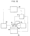
- Fig. 12 shows a block diagram of an STM apparatus manufactured by using the parallel plane holding mechanism of the invention.
- a probe 83 is allowed to approach a sample 82 by a cantilever type probe 81 of the cantilever beam shape used in the embodiment 2 (z direction).
- the x direction in the plane of the sample 82 is scanned by a piezoelectric Bimorph mechanism provided in the cantilever and the y direction is scanned by an XY stage 84.
- Voltages are applied to the probe 83 and the sample 82 by a bias voltage applying circuit 85.
- a tunnel current which is observed at this time is read out by a tunnel current detecting amplifying circuit 86, thereby observing an image.
- a parallel plane holding mechanism 89 of the invention is arranged on the XY stage.
- the sample is fixed onto the holding mechanism 89.
- the distance between the sample 82 and the probe 83 is controlled by the Z control of the cantilever type probe and the parallel plane holding mechanism 89.
- the actuation of the XY stage 84 is controlled by a drive control circuit 87.
- a sequence control of the above circuits is executed by a CPU 88.
- a control mechanism such as a scanning mechanism by the XY stage 84, a control mechanism such as cylindrical piezoelectric actuator, parallel spring, differential micrometer, voice coil, inch worm, or the like is used.
- the memory device using the parallel plane holding mechanism comprises: the structure having the beams made of the elastic members in the peripheral portion of the plane-shaped weight; the base plate arranged so as to face the weight; and the electrodes arranged on the opposite surfaces of the weight and the base plate, wherein the distance between the weight and the base plate is controlled by applying the voltages to the electrodes, the structure and/or the object to be driven which is connected to the base plate are/is moved, thereby arbitrarily keeping the reference surface of the object in parallel with a predetermined reference surface, the structure is set to either one of the recording head and the recording medium, and the predetermined reference surface is set to the other one of the recording medium and the recording head.
- the STM apparatus using the parallel plane holding mechanism comprises: the structure having the beams made of the elastic members in the peripheral portion of the plane-shaped weight; the base plate arranged so as to face the weight; and the electrodes arranged on the opposite surfaces of the weight and the base plate, whereby the distance between the weight and the base plate is controlled by applying the voltages to the electrodes, the structure and/or the object to be driven which is connected to the base plate is moved, thereby arbitrarily keeping the reference surface of the object in parallel with a predetermined reference surface, the structure is set to either one of the stylus to measure and sense and the object to be measured, and the predetermined reference surface is set to the other one of the measuring object and the stylus.
- the parallel plane holding mechanism according to the invention and the apparatus using such a mechanism are effective for the parallel plane holding mechanism to hold the parallel plane and have an effect such that the noises are reduced when they are applied to the recording head to access to the recording medium.
- the probe and the recording medium or the recording head can be integrated together with an IC and a miniaturization can be realized. With respect to the STM as well, the miniaturization can be realized.
Landscapes
- Physics & Mathematics (AREA)
- General Physics & Mathematics (AREA)
- Chemical & Material Sciences (AREA)
- General Health & Medical Sciences (AREA)
- Nuclear Medicine, Radiotherapy & Molecular Imaging (AREA)
- Radiology & Medical Imaging (AREA)
- Health & Medical Sciences (AREA)
- Engineering & Computer Science (AREA)
- Nanotechnology (AREA)
- Analytical Chemistry (AREA)
- Crystallography & Structural Chemistry (AREA)
- Micromachines (AREA)
- Spinning Or Twisting Of Yarns (AREA)
- Semiconductor Memories (AREA)
- Manufacture Or Reproduction Of Printing Formes (AREA)
Applications Claiming Priority (4)
| Application Number | Priority Date | Filing Date | Title |
|---|---|---|---|
| JP273289/91 | 1991-09-24 | ||
| JP27328991 | 1991-09-24 | ||
| JP238366/92 | 1992-09-07 | ||
| JP23836692A JP3184619B2 (ja) | 1991-09-24 | 1992-09-07 | 平行平面保持機構及びそれを用いたメモリ装置及びstm装置 |
Publications (2)
| Publication Number | Publication Date |
|---|---|
| EP0534406A1 true EP0534406A1 (de) | 1993-03-31 |
| EP0534406B1 EP0534406B1 (de) | 1997-04-09 |
Family
ID=26533658
Family Applications (1)
| Application Number | Title | Priority Date | Filing Date |
|---|---|---|---|
| EP92116287A Expired - Lifetime EP0534406B1 (de) | 1991-09-24 | 1992-09-23 | Mechanismus zum parallelen Halten einer Fläche und Apparat zur Verwendung eines solchen Mechanismus |
Country Status (5)
| Country | Link |
|---|---|
| US (1) | US5554851A (de) |
| EP (1) | EP0534406B1 (de) |
| JP (1) | JP3184619B2 (de) |
| AT (1) | ATE151523T1 (de) |
| DE (1) | DE69218866T2 (de) |
Cited By (3)
| Publication number | Priority date | Publication date | Assignee | Title |
|---|---|---|---|---|
| EP0665590A3 (de) * | 1994-01-31 | 1996-02-07 | Canon Kk | Mikromechanisches Element, Herstellungsverfahren dafür und Vorrichtungen mit diesem Element. |
| EP0711029A3 (de) * | 1994-11-07 | 1996-10-02 | Canon Kk | Mikrostruktur und Verfahren zu deren Herstellung |
| EP0703429A3 (de) * | 1994-09-21 | 1996-10-16 | Canon Kk | Probe mit Torsionshebel-Struktur und Abtast-Proben-Mikroskop und Apparat zur Aufnahme/Wiedergabe bei seiner Benutzung |
Families Citing this family (19)
| Publication number | Priority date | Publication date | Assignee | Title |
|---|---|---|---|---|
| US5949892A (en) * | 1995-12-07 | 1999-09-07 | Advanced Micro Devices, Inc. | Method of and apparatus for dynamically controlling operating characteristics of a microphone |
| JPH09293283A (ja) * | 1996-04-25 | 1997-11-11 | Hewlett Packard Co <Hp> | プローブ装置およびその製造方法、ならびにメディア移動型メモリ装置 |
| JPH10312592A (ja) * | 1997-05-13 | 1998-11-24 | Canon Inc | 情報処理装置および情報処理方法 |
| US5963367A (en) * | 1997-09-23 | 1999-10-05 | Lucent Technologies, Inc. | Micromechanical xyz stage for use with optical elements |
| US6215222B1 (en) * | 1999-03-30 | 2001-04-10 | Agilent Technologies, Inc. | Optical cross-connect switch using electrostatic surface actuators |
| AU7289801A (en) * | 2000-04-11 | 2001-10-23 | Sandia Corp | Microelectromechanical apparatus for elevating and tilting a platform |
| WO2002052894A1 (en) * | 2000-12-22 | 2002-07-04 | Brüel & Kjær Sound & Vibration Measurement A/S | A micromachined capacitive transducer |
| US6831765B2 (en) * | 2001-02-22 | 2004-12-14 | Canon Kabushiki Kaisha | Tiltable-body apparatus, and method of fabricating the same |
| JP4036643B2 (ja) | 2001-12-21 | 2008-01-23 | オリンパス株式会社 | 光偏向器及び光偏向器アレイ |
| US6717325B2 (en) * | 2002-03-06 | 2004-04-06 | Glimmerglass Networks, Inc. | Method and apparatus for actuation of a two-axis MEMS device using three actuation elements |
| JP4025990B2 (ja) * | 2002-09-26 | 2007-12-26 | セイコーエプソン株式会社 | ミラーデバイス、光スイッチ、電子機器およびミラーデバイス駆動方法 |
| JP5027984B2 (ja) * | 2003-03-28 | 2012-09-19 | キヤノン株式会社 | 揺動体を用いた電位測定装置、電位測定方法、及び画像形成装置 |
| JP2004301554A (ja) * | 2003-03-28 | 2004-10-28 | Canon Inc | 電位測定装置及び画像形成装置 |
| FR2868411B1 (fr) * | 2004-04-01 | 2006-06-16 | Commissariat Energie Atomique | Membrane souple comportant des entailles |
| FR2869027B1 (fr) * | 2004-04-15 | 2006-07-14 | Commissariat Energie Atomique | Systeme d'enregistrement comportant une couche memoire et un reseau de micro-pointes |
| JP2006317358A (ja) * | 2005-05-16 | 2006-11-24 | Canon Inc | 電位測定装置、およびそれを用いた画像形成装置 |
| US7382137B2 (en) * | 2005-05-27 | 2008-06-03 | Canon Kabushiki Kaisha | Potential measuring apparatus |
| JP5188024B2 (ja) * | 2006-02-09 | 2013-04-24 | キヤノン株式会社 | 揺動体装置、電位測定装置、及び光偏向装置 |
| KR101982506B1 (ko) * | 2017-11-17 | 2019-09-10 | 인하대학교 산학협력단 | 평탄도 조절장치 |
Citations (7)
| Publication number | Priority date | Publication date | Assignee | Title |
|---|---|---|---|---|
| WO1989012830A2 (en) * | 1988-06-20 | 1989-12-28 | Triton Technologies, Inc. | Micro-machined accelerometer |
| EP0363550A1 (de) * | 1988-10-14 | 1990-04-18 | International Business Machines Corporation | Abstandsgesteuerter Tunneleffektwandler und den Wandler verwendende Speichereinheit mit direktem Zugriff |
| EP0368579A2 (de) * | 1988-11-09 | 1990-05-16 | Canon Kabushiki Kaisha | Sondeneinheit, Betriebsverfahren und Rastervorrichtung zur Feststellung eines Tunnelstromes mit dieser Sonde |
| DE4022711A1 (de) * | 1989-07-17 | 1991-01-31 | Olympus Optical Co | Tunnelstromsonden-verstellvorrichtung |
| US5006487A (en) * | 1989-07-27 | 1991-04-09 | Honeywell Inc. | Method of making an electrostatic silicon accelerometer |
| EP0487003A2 (de) * | 1990-11-20 | 1992-05-27 | Canon Kabushiki Kaisha | Neigungswinkelbestimmungsverfahren sowie Informationsbestimmungsschreibvorrichtung dafür |
| EP0491973A1 (de) * | 1990-12-21 | 1992-07-01 | International Business Machines Corporation | Integriertes Rastertunnelmikroskop mit pneumatischer und elektrostatischer Steuerung und Verfahren zum Herstellen desselben |
Family Cites Families (7)
| Publication number | Priority date | Publication date | Assignee | Title |
|---|---|---|---|---|
| US4381672A (en) * | 1981-03-04 | 1983-05-03 | The Bendix Corporation | Vibrating beam rotation sensor |
| DE3572030D1 (en) * | 1985-03-07 | 1989-09-07 | Ibm | Scanning tunneling microscope |
| DE3679319D1 (de) * | 1986-05-27 | 1991-06-20 | Ibm | Speichereinheit mit direktem zugriff. |
| EP0262253A1 (de) * | 1986-10-03 | 1988-04-06 | International Business Machines Corporation | Mikromechanische Fühlervorrichtung für atomare Kräfte |
| JP2556491B2 (ja) * | 1986-12-24 | 1996-11-20 | キヤノン株式会社 | 記録装置及び記録法 |
| GB8826457D0 (en) * | 1988-11-11 | 1988-12-14 | Ici Plc | Thermal transfer receiver |
| US5051643A (en) * | 1990-08-30 | 1991-09-24 | Motorola, Inc. | Electrostatically switched integrated relay and capacitor |
-
1992
- 1992-09-07 JP JP23836692A patent/JP3184619B2/ja not_active Expired - Fee Related
- 1992-09-23 AT AT92116287T patent/ATE151523T1/de not_active IP Right Cessation
- 1992-09-23 DE DE69218866T patent/DE69218866T2/de not_active Expired - Lifetime
- 1992-09-23 EP EP92116287A patent/EP0534406B1/de not_active Expired - Lifetime
-
1995
- 1995-03-20 US US08/407,245 patent/US5554851A/en not_active Expired - Lifetime
Patent Citations (7)
| Publication number | Priority date | Publication date | Assignee | Title |
|---|---|---|---|---|
| WO1989012830A2 (en) * | 1988-06-20 | 1989-12-28 | Triton Technologies, Inc. | Micro-machined accelerometer |
| EP0363550A1 (de) * | 1988-10-14 | 1990-04-18 | International Business Machines Corporation | Abstandsgesteuerter Tunneleffektwandler und den Wandler verwendende Speichereinheit mit direktem Zugriff |
| EP0368579A2 (de) * | 1988-11-09 | 1990-05-16 | Canon Kabushiki Kaisha | Sondeneinheit, Betriebsverfahren und Rastervorrichtung zur Feststellung eines Tunnelstromes mit dieser Sonde |
| DE4022711A1 (de) * | 1989-07-17 | 1991-01-31 | Olympus Optical Co | Tunnelstromsonden-verstellvorrichtung |
| US5006487A (en) * | 1989-07-27 | 1991-04-09 | Honeywell Inc. | Method of making an electrostatic silicon accelerometer |
| EP0487003A2 (de) * | 1990-11-20 | 1992-05-27 | Canon Kabushiki Kaisha | Neigungswinkelbestimmungsverfahren sowie Informationsbestimmungsschreibvorrichtung dafür |
| EP0491973A1 (de) * | 1990-12-21 | 1992-07-01 | International Business Machines Corporation | Integriertes Rastertunnelmikroskop mit pneumatischer und elektrostatischer Steuerung und Verfahren zum Herstellen desselben |
Cited By (5)
| Publication number | Priority date | Publication date | Assignee | Title |
|---|---|---|---|---|
| EP0665590A3 (de) * | 1994-01-31 | 1996-02-07 | Canon Kk | Mikromechanisches Element, Herstellungsverfahren dafür und Vorrichtungen mit diesem Element. |
| US5658698A (en) * | 1994-01-31 | 1997-08-19 | Canon Kabushiki Kaisha | Microstructure, process for manufacturing thereof and devices incorporating the same |
| EP0703429A3 (de) * | 1994-09-21 | 1996-10-16 | Canon Kk | Probe mit Torsionshebel-Struktur und Abtast-Proben-Mikroskop und Apparat zur Aufnahme/Wiedergabe bei seiner Benutzung |
| EP0711029A3 (de) * | 1994-11-07 | 1996-10-02 | Canon Kk | Mikrostruktur und Verfahren zu deren Herstellung |
| US5994750A (en) * | 1994-11-07 | 1999-11-30 | Canon Kabushiki Kaisha | Microstructure and method of forming the same |
Also Published As
| Publication number | Publication date |
|---|---|
| ATE151523T1 (de) | 1997-04-15 |
| JPH05225620A (ja) | 1993-09-03 |
| US5554851A (en) | 1996-09-10 |
| JP3184619B2 (ja) | 2001-07-09 |
| EP0534406B1 (de) | 1997-04-09 |
| DE69218866D1 (de) | 1997-05-15 |
| DE69218866T2 (de) | 1997-10-09 |
Similar Documents
| Publication | Publication Date | Title |
|---|---|---|
| US5554851A (en) | Parallel plane holding mechanism and apparatus using such a mechanism | |
| EP0452852B1 (de) | Gerät zur Informationsaufzeichnung und/oder -wiedergabe | |
| JP3060137B2 (ja) | カンチレバー型プローブの作製方法 | |
| US5412641A (en) | Information recording/reproducing apparatus for recording/reproducing information with probes | |
| JP3450349B2 (ja) | カンチレバー型プローブ | |
| JP2566653B2 (ja) | 間隔制御トンネリング変換器 | |
| EP0391429B1 (de) | Vorrichtung zur Erfassung von Mikroverschiebungen, Piezo-Stellantrieb unter Verwendung der Vorrichtung und Abtastmikroskop unter Verwendung des Piezo-Stellantriebes | |
| JPH04147448A (ja) | カンチレバー型プローブ、それを用いた走査型トンネル顕微鏡及び情報処理装置 | |
| US5717680A (en) | Information processing apparatus with mechanism for adjusting interval between substrate for supporting a plurality of probes and recording medium | |
| US5371728A (en) | Information recording/reproducing apparatus using probe | |
| JP3088576B2 (ja) | 集積化アクチュエータを備えた走査型トンネル顕微鏡および前記集積化アクチュエータを備えた情報処理装置 | |
| JPH04350510A (ja) | マルチプローブユニット、情報処理装置、走査型トンネル顕微鏡、カンチレバー型プローブ | |
| JP3226424B2 (ja) | 走査型プローブ顕微鏡ならびに該顕微鏡を用いた加工装置および情報処理装置 | |
| JP3053971B2 (ja) | トンネル電流発生用三次元変位素子、該トンネル電流発生用三次元変位素子を用いたマルチ探針ユニット、および情報処理装置 | |
| JP2890268B2 (ja) | プローブユニット及びこれを用いた情報処理装置と走査型トンネル顕微鏡 | |
| JP3060142B2 (ja) | カンチレバー型変位素子の駆動方法、走査型トンネル顕微鏡、情報処理装置、及びカンチレバー型変位素子 | |
| JP3234722B2 (ja) | 円弧状反りレバー型アクチュエータ、該アクチュエータの駆動方法及び情報入出力用プローブを用いた情報処理装置 | |
| JP3234952B2 (ja) | プローブユニット及びこれを用いた走査型トンネル顕微鏡、情報処理装置 | |
| JP3042817B2 (ja) | 情報記録再生装置における相対位置合わせ装置及び方法 | |
| JP2934037B2 (ja) | 情報記録及び/又は再生装置 | |
| JPH06139629A (ja) | 情報記録坦体およびこれを使用する情報処理装置 | |
| JPH07110969A (ja) | 面合わせ方法,位置制御機構および該機構を有する情報処理装置 | |
| JP2962612B2 (ja) | 走査顕微鏡 | |
| JPH04223204A (ja) | プローブユニット及びこれを用いた情報処理装置 | |
| JPH08263885A (ja) | 情報処理装置 |
Legal Events
| Date | Code | Title | Description |
|---|---|---|---|
| PUAI | Public reference made under article 153(3) epc to a published international application that has entered the european phase |
Free format text: ORIGINAL CODE: 0009012 |
|
| AK | Designated contracting states |
Kind code of ref document: A1 Designated state(s): AT BE CH DE DK ES FR GB GR IT LI LU MC NL PT SE |
|
| 17P | Request for examination filed |
Effective date: 19930817 |
|
| 17Q | First examination report despatched |
Effective date: 19941027 |
|
| GRAG | Despatch of communication of intention to grant |
Free format text: ORIGINAL CODE: EPIDOS AGRA |
|
| GRAH | Despatch of communication of intention to grant a patent |
Free format text: ORIGINAL CODE: EPIDOS IGRA |
|
| GRAH | Despatch of communication of intention to grant a patent |
Free format text: ORIGINAL CODE: EPIDOS IGRA |
|
| GRAA | (expected) grant |
Free format text: ORIGINAL CODE: 0009210 |
|
| AK | Designated contracting states |
Kind code of ref document: B1 Designated state(s): AT BE CH DE DK ES FR GB GR IT LI LU MC NL PT SE |
|
| PG25 | Lapsed in a contracting state [announced via postgrant information from national office to epo] |
Ref country code: IT Free format text: LAPSE BECAUSE OF FAILURE TO SUBMIT A TRANSLATION OF THE DESCRIPTION OR TO PAY THE FEE WITHIN THE PRESCRIBED TIME-LIMIT;WARNING: LAPSES OF ITALIAN PATENTS WITH EFFECTIVE DATE BEFORE 2007 MAY HAVE OCCURRED AT ANY TIME BEFORE 2007. THE CORRECT EFFECTIVE DATE MAY BE DIFFERENT FROM THE ONE RECORDED. Effective date: 19970409 Ref country code: AT Effective date: 19970409 Ref country code: ES Free format text: THE PATENT HAS BEEN ANNULLED BY A DECISION OF A NATIONAL AUTHORITY Effective date: 19970409 Ref country code: DK Effective date: 19970409 Ref country code: GR Free format text: LAPSE BECAUSE OF FAILURE TO SUBMIT A TRANSLATION OF THE DESCRIPTION OR TO PAY THE FEE WITHIN THE PRESCRIBED TIME-LIMIT Effective date: 19970409 |
|
| REF | Corresponds to: |
Ref document number: 151523 Country of ref document: AT Date of ref document: 19970415 Kind code of ref document: T |
|
| REG | Reference to a national code |
Ref country code: CH Ref legal event code: NV Representative=s name: BOVARD AG PATENTANWAELTE Ref country code: CH Ref legal event code: EP |
|
| REF | Corresponds to: |
Ref document number: 69218866 Country of ref document: DE Date of ref document: 19970515 |
|
| ET | Fr: translation filed | ||
| PG25 | Lapsed in a contracting state [announced via postgrant information from national office to epo] |
Ref country code: PT Effective date: 19970709 |
|
| PG25 | Lapsed in a contracting state [announced via postgrant information from national office to epo] |
Ref country code: LU Free format text: LAPSE BECAUSE OF NON-PAYMENT OF DUE FEES Effective date: 19970923 |
|
| PLBE | No opposition filed within time limit |
Free format text: ORIGINAL CODE: 0009261 |
|
| PG25 | Lapsed in a contracting state [announced via postgrant information from national office to epo] |
Ref country code: MC Free format text: LAPSE BECAUSE OF NON-PAYMENT OF DUE FEES Effective date: 19980331 |
|
| 26N | No opposition filed | ||
| REG | Reference to a national code |
Ref country code: GB Ref legal event code: IF02 |
|
| PGFP | Annual fee paid to national office [announced via postgrant information from national office to epo] |
Ref country code: CH Payment date: 20070913 Year of fee payment: 16 |
|
| PGFP | Annual fee paid to national office [announced via postgrant information from national office to epo] |
Ref country code: SE Payment date: 20070905 Year of fee payment: 16 Ref country code: NL Payment date: 20070916 Year of fee payment: 16 |
|
| PGFP | Annual fee paid to national office [announced via postgrant information from national office to epo] |
Ref country code: BE Payment date: 20071120 Year of fee payment: 16 |
|
| PGFP | Annual fee paid to national office [announced via postgrant information from national office to epo] |
Ref country code: FR Payment date: 20070914 Year of fee payment: 16 |
|
| BERE | Be: lapsed |
Owner name: *CANON K.K. Effective date: 20080930 |
|
| REG | Reference to a national code |
Ref country code: CH Ref legal event code: PL |
|
| PG25 | Lapsed in a contracting state [announced via postgrant information from national office to epo] |
Ref country code: NL Free format text: LAPSE BECAUSE OF NON-PAYMENT OF DUE FEES Effective date: 20090401 |
|
| NLV4 | Nl: lapsed or anulled due to non-payment of the annual fee |
Effective date: 20090401 |
|
| REG | Reference to a national code |
Ref country code: FR Ref legal event code: ST Effective date: 20090529 |
|
| PG25 | Lapsed in a contracting state [announced via postgrant information from national office to epo] |
Ref country code: BE Free format text: LAPSE BECAUSE OF NON-PAYMENT OF DUE FEES Effective date: 20080930 |
|
| PG25 | Lapsed in a contracting state [announced via postgrant information from national office to epo] |
Ref country code: FR Free format text: LAPSE BECAUSE OF NON-PAYMENT OF DUE FEES Effective date: 20080930 Ref country code: LI Free format text: LAPSE BECAUSE OF NON-PAYMENT OF DUE FEES Effective date: 20080930 Ref country code: CH Free format text: LAPSE BECAUSE OF NON-PAYMENT OF DUE FEES Effective date: 20080930 |
|
| PG25 | Lapsed in a contracting state [announced via postgrant information from national office to epo] |
Ref country code: SE Free format text: LAPSE BECAUSE OF NON-PAYMENT OF DUE FEES Effective date: 20080924 |
|
| PGFP | Annual fee paid to national office [announced via postgrant information from national office to epo] |
Ref country code: GB Payment date: 20100928 Year of fee payment: 19 |
|
| PGFP | Annual fee paid to national office [announced via postgrant information from national office to epo] |
Ref country code: DE Payment date: 20100930 Year of fee payment: 19 |
|
| GBPC | Gb: european patent ceased through non-payment of renewal fee |
Effective date: 20110923 |
|
| REG | Reference to a national code |
Ref country code: DE Ref legal event code: R119 Ref document number: 69218866 Country of ref document: DE Effective date: 20120403 |
|
| PG25 | Lapsed in a contracting state [announced via postgrant information from national office to epo] |
Ref country code: DE Free format text: LAPSE BECAUSE OF NON-PAYMENT OF DUE FEES Effective date: 20120403 |
|
| PG25 | Lapsed in a contracting state [announced via postgrant information from national office to epo] |
Ref country code: GB Free format text: LAPSE BECAUSE OF NON-PAYMENT OF DUE FEES Effective date: 20110923 |