EP0535681A2 - Halbleiterkörper, Verfahren zu seiner Herstellung und Halbleiteranordnung mit diesem Körper - Google Patents
Halbleiterkörper, Verfahren zu seiner Herstellung und Halbleiteranordnung mit diesem Körper Download PDFInfo
- Publication number
- EP0535681A2 EP0535681A2 EP92116847A EP92116847A EP0535681A2 EP 0535681 A2 EP0535681 A2 EP 0535681A2 EP 92116847 A EP92116847 A EP 92116847A EP 92116847 A EP92116847 A EP 92116847A EP 0535681 A2 EP0535681 A2 EP 0535681A2
- Authority
- EP
- European Patent Office
- Prior art keywords
- semiconductor
- main surface
- semiconductor substrate
- element formation
- insulated
- Prior art date
- Legal status (The legal status is an assumption and is not a legal conclusion. Google has not performed a legal analysis and makes no representation as to the accuracy of the status listed.)
- Granted
Links
Images


Classifications
-
- H—ELECTRICITY
- H10—SEMICONDUCTOR DEVICES; ELECTRIC SOLID-STATE DEVICES NOT OTHERWISE PROVIDED FOR
- H10P—GENERIC PROCESSES OR APPARATUS FOR THE MANUFACTURE OR TREATMENT OF DEVICES COVERED BY CLASS H10
- H10P14/00—Formation of materials, e.g. in the shape of layers or pillars
- H10P14/60—Formation of materials, e.g. in the shape of layers or pillars of insulating materials
- H10P14/63—Formation of materials, e.g. in the shape of layers or pillars of insulating materials characterised by the formation processes
- H10P14/6302—Non-deposition formation processes
- H10P14/6304—Formation by oxidation, e.g. oxidation of the substrate
- H10P14/6306—Formation by oxidation, e.g. oxidation of the substrate of the semiconductor materials
- H10P14/6308—Formation by oxidation, e.g. oxidation of the substrate of the semiconductor materials of Group IV semiconductors
- H10P14/6309—Formation by oxidation, e.g. oxidation of the substrate of the semiconductor materials of Group IV semiconductors of silicon in uncombined form, i.e. pure silicon
-
- H—ELECTRICITY
- H10—SEMICONDUCTOR DEVICES; ELECTRIC SOLID-STATE DEVICES NOT OTHERWISE PROVIDED FOR
- H10B—ELECTRONIC MEMORY DEVICES
- H10B10/00—Static random access memory [SRAM] devices
-
- H—ELECTRICITY
- H10—SEMICONDUCTOR DEVICES; ELECTRIC SOLID-STATE DEVICES NOT OTHERWISE PROVIDED FOR
- H10D—INORGANIC ELECTRIC SEMICONDUCTOR DEVICES
- H10D84/00—Integrated devices formed in or on semiconductor substrates that comprise only semiconducting layers, e.g. on Si wafers or on GaAs-on-Si wafers
- H10D84/01—Manufacture or treatment
- H10D84/0123—Integrating together multiple components covered by H10D12/00 or H10D30/00, e.g. integrating multiple IGBTs
- H10D84/0126—Integrating together multiple components covered by H10D12/00 or H10D30/00, e.g. integrating multiple IGBTs the components including insulated gates, e.g. IGFETs
- H10D84/0165—Integrating together multiple components covered by H10D12/00 or H10D30/00, e.g. integrating multiple IGBTs the components including insulated gates, e.g. IGFETs the components including complementary IGFETs, e.g. CMOS devices
- H10D84/0191—Manufacturing their doped wells
-
- H—ELECTRICITY
- H10—SEMICONDUCTOR DEVICES; ELECTRIC SOLID-STATE DEVICES NOT OTHERWISE PROVIDED FOR
- H10D—INORGANIC ELECTRIC SEMICONDUCTOR DEVICES
- H10D84/00—Integrated devices formed in or on semiconductor substrates that comprise only semiconducting layers, e.g. on Si wafers or on GaAs-on-Si wafers
- H10D84/01—Manufacture or treatment
- H10D84/02—Manufacture or treatment characterised by using material-based technologies
- H10D84/03—Manufacture or treatment characterised by using material-based technologies using Group IV technology, e.g. silicon technology or silicon-carbide [SiC] technology
- H10D84/038—Manufacture or treatment characterised by using material-based technologies using Group IV technology, e.g. silicon technology or silicon-carbide [SiC] technology using silicon technology, e.g. SiGe
-
- H—ELECTRICITY
- H10—SEMICONDUCTOR DEVICES; ELECTRIC SOLID-STATE DEVICES NOT OTHERWISE PROVIDED FOR
- H10D—INORGANIC ELECTRIC SEMICONDUCTOR DEVICES
- H10D84/00—Integrated devices formed in or on semiconductor substrates that comprise only semiconducting layers, e.g. on Si wafers or on GaAs-on-Si wafers
- H10D84/80—Integrated devices formed in or on semiconductor substrates that comprise only semiconducting layers, e.g. on Si wafers or on GaAs-on-Si wafers characterised by the integration of at least one component covered by groups H10D12/00 or H10D30/00, e.g. integration of IGFETs
- H10D84/82—Integrated devices formed in or on semiconductor substrates that comprise only semiconducting layers, e.g. on Si wafers or on GaAs-on-Si wafers characterised by the integration of at least one component covered by groups H10D12/00 or H10D30/00, e.g. integration of IGFETs of only field-effect components
- H10D84/83—Integrated devices formed in or on semiconductor substrates that comprise only semiconducting layers, e.g. on Si wafers or on GaAs-on-Si wafers characterised by the integration of at least one component covered by groups H10D12/00 or H10D30/00, e.g. integration of IGFETs of only field-effect components of only insulated-gate FETs [IGFET]
- H10D84/85—Complementary IGFETs, e.g. CMOS
- H10D84/859—Complementary IGFETs, e.g. CMOS comprising both N-type and P-type wells, e.g. twin-tub
-
- H—ELECTRICITY
- H10—SEMICONDUCTOR DEVICES; ELECTRIC SOLID-STATE DEVICES NOT OTHERWISE PROVIDED FOR
- H10P—GENERIC PROCESSES OR APPARATUS FOR THE MANUFACTURE OR TREATMENT OF DEVICES COVERED BY CLASS H10
- H10P10/00—Bonding of wafers, substrates or parts of devices
- H10P10/12—Bonding of semiconductor wafers or semiconductor substrates to semiconductor wafers or semiconductor substrates
- H10P10/128—Bonding of semiconductor wafers or semiconductor substrates to semiconductor wafers or semiconductor substrates by direct semiconductor to semiconductor bonding
-
- H—ELECTRICITY
- H10—SEMICONDUCTOR DEVICES; ELECTRIC SOLID-STATE DEVICES NOT OTHERWISE PROVIDED FOR
- H10P—GENERIC PROCESSES OR APPARATUS FOR THE MANUFACTURE OR TREATMENT OF DEVICES COVERED BY CLASS H10
- H10P14/00—Formation of materials, e.g. in the shape of layers or pillars
- H10P14/60—Formation of materials, e.g. in the shape of layers or pillars of insulating materials
- H10P14/63—Formation of materials, e.g. in the shape of layers or pillars of insulating materials characterised by the formation processes
- H10P14/6302—Non-deposition formation processes
- H10P14/6322—Formation by thermal treatments
-
- H—ELECTRICITY
- H10—SEMICONDUCTOR DEVICES; ELECTRIC SOLID-STATE DEVICES NOT OTHERWISE PROVIDED FOR
- H10W—GENERIC PACKAGES, INTERCONNECTIONS, CONNECTORS OR OTHER CONSTRUCTIONAL DETAILS OF DEVICES COVERED BY CLASS H10
- H10W10/00—Isolation regions in semiconductor bodies between components of integrated devices
- H10W10/01—Manufacture or treatment
- H10W10/011—Manufacture or treatment of isolation regions comprising dielectric materials
- H10W10/012—Manufacture or treatment of isolation regions comprising dielectric materials using local oxidation of silicon [LOCOS]
- H10W10/0121—Manufacture or treatment of isolation regions comprising dielectric materials using local oxidation of silicon [LOCOS] in regions recessed from the surface, e.g. in trenches or grooves
-
- H—ELECTRICITY
- H10—SEMICONDUCTOR DEVICES; ELECTRIC SOLID-STATE DEVICES NOT OTHERWISE PROVIDED FOR
- H10W—GENERIC PACKAGES, INTERCONNECTIONS, CONNECTORS OR OTHER CONSTRUCTIONAL DETAILS OF DEVICES COVERED BY CLASS H10
- H10W10/00—Isolation regions in semiconductor bodies between components of integrated devices
- H10W10/01—Manufacture or treatment
- H10W10/011—Manufacture or treatment of isolation regions comprising dielectric materials
- H10W10/018—Manufacture or treatment of isolation regions comprising dielectric materials using selective deposition of crystalline silicon, e.g. using epitaxial growth of silicon
-
- H—ELECTRICITY
- H10—SEMICONDUCTOR DEVICES; ELECTRIC SOLID-STATE DEVICES NOT OTHERWISE PROVIDED FOR
- H10W—GENERIC PACKAGES, INTERCONNECTIONS, CONNECTORS OR OTHER CONSTRUCTIONAL DETAILS OF DEVICES COVERED BY CLASS H10
- H10W10/00—Isolation regions in semiconductor bodies between components of integrated devices
- H10W10/10—Isolation regions comprising dielectric materials
- H10W10/13—Isolation regions comprising dielectric materials formed using local oxidation of silicon [LOCOS], e.g. sealed interface localised oxidation [SILO] or side-wall mask isolation [SWAMI]
Definitions
- This invention relates to a semiconductor body, its manufacturing method, and a semiconductor device using the body, and more particularly to a semiconductor body capable of optimizing the performance and characteristics of active elements.
- the n-channel MOSFET hereinafter, referred to as the NMOS
- the PMOS p-channel MOSFET
- MOS transistor's characteristics including transconductance and reliability depend on the surface orientation of the substrate. Thus, it is impossible to optimize the performance and characteristics of semiconductor elements in the present-day semiconductor substrate (body). That is, CMOS semiconductor devices forming present-day NMOS and PMOS transistors have not yet drawn their maximum performance.
- the object of the present invention is to provide a semiconductor body capable of allowing semiconductor elements of different conductivity types not only to simultaneously display their full performance but also to form semiconductor elements with the optimum characteristics into a device, its manufacturing method, and a semiconductor device using the body.
- a semiconductor body of the present invention contains a portion having a first surface orientation, and a portion having a second surface orientation almost parallel to the first portion.
- the semiconductor body has the first surface orientation portion and the second orientation portion almost parallel to the first portion, forming semiconductor elements of different conductivity types in the first and second surface orientation portions, respectively, makes it possible to maximize the performance of those semiconductor elements of different conductivity types at the same time.
- the semiconductor element formed in the first surface orientation portion differs from that in the second surface orientation portion in the performance and characteristics. This makes it possible to form semiconductor elements with the optimum characteristics into a semiconductor device by forming the semiconductor element either in the first or the second surface orientation portion, depending on the requirements.
- the semiconductor device thus formed has several advantages such as the improved performance.
- a concrete method of forming the above semiconductor body is first to prepare a first semiconductor substrate whose main surface has a first surface orientation, and a second semiconductor substrate whose main surface has a second surface orientation, and then laminate the main surface of the first semiconductor substrate to that of the second semiconductor substrate, and finally make at least one opening in the first semiconductor substrate so that the second semiconductor substrate may be exposed.
- Figs. 1A to 1F are sectional views in the manufacturing sequence of a semiconductor device according to a first embodiment of the present invention.
- First prepared are a single-crystal silicon substrate (wafer) 10 in which the (100) plane appears at the main surface and a single-crystal silicon substrate (wafer) 12 in which the (110) plane comes out to the main surface (Fig. 1A).
- the substrate 10 is laminated to the substrate 12 to form a silicon body 20 (Fig. 1B).
- the lamination of those two substrates is carried out by, for example, planishing adhesion techniques.
- a mask material 14 made of, for example, a silicon oxide film is deposited.
- a photoresist (not shown) is applied over the mask material 14 to form a photoresist layer. Patterning is done on the photoresist layer by the photoetching method to make a window in the photoresist layer in order to form an opening.
- the mask material 14 is then etched, using the photoresist layer as a mask. This forms a window 16 in the mask material 14 at which the main surface of the substrate 10 is exposed. With the mask material 14 as a mask, the substrate 10 is etched to form an opening 18 that allows the main surface of the substrate 12 to be exposed (Fig. 1C).
- the substrate 10 may be polished to reduce its film thickness.
- the silicon body 20 has portions of different surface orientations: a portion where the (100) plane is exposed and a portion where the (110) plane is exposed. Since these planes are almost parallel to each other, semiconductor elements can be formed at the (100) plane and the (110) plane, in the same manner as with a normal wafer (Fig. 1D).
- p-type impurities are introduced into the substrate 10 with the (100) surface orientation.
- n-type impurities are then introduced into the substrate 12 with the (110) surface orientation.
- the introduced impurities are activated to form a p-type well 22 in the substrate 10, and an n-type well 24 in the substrate 12 (Fig. 1E).
- NMOS 26 is formed in the p-type well 22, and a PMPS 28 is formed in the n-type well 24. This completes the semiconductor device of the first embodiment (Fig. 1F).
- the silicon body 20 has a plurality of different surface orientation portions, in which NMOSes and PMOSes are formed so as to achieve their maximum performance, thereby providing a high-performance semiconductor device.
- a PMOS is formed in the substrate 10 with the (100) surface orientation
- an NMOS is formed in the substrate 12 with the (110) surface orientation.
- Packing such semiconductor devices into an integrated circuit provides a high-performance semiconductor integrated circuit device.
- Figs. 2A to 2E are sectional views in the manufacturing sequence of a semiconductor device according to a second embodiment of the present invention.
- First prepared are a p-type single-crystal silicon substrate (wafer) 30 in which the (100) plane comes out to the main surface and an n-type single-crystal silicon substrate (wafer) 32 in which the (110) plane appear at the main surface (Fig. 2A).
- the substrate 30 is laminated to the substrate 32 by, for example, planishing adhesion techniques to form a silicon body 40 (Fig. 2B).
- a mask material 14 with a window composed of, for example, a silicon oxide film, is formed on the p-type substrate 30.
- the p-type substrate 30 is etched to make an opening 18 that allows the main surface of the n-type substrate 32 to appear at the bottom (Fig. 2C).
- the silicon body 40 has portions of different surface orientations: a portion with the (100) plane and a portion with the (110) plane. Further, in the present embodiment, the portions of different surface orientations are of different conductivity types (Fig. 2D).
- NMOS 26 is formed in the p-type substrate 30, and a PMOS 28 is formed in the n-type substrate 32. This completes the semiconductor device of the second embodiment (Fig. 2E).
- NMOS and PMOS in the portions with surface orientations that enable their best performance to be achieved, a high-performance semiconductor device can be made.
- Making the conductivity types of the two substrate 30 and 32 different permits the omission of the well formation process, simplifying the manufacturing processes.
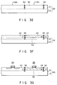
- Figs. 3A to 3G are sectional views in the manufacturing sequence of a semiconductor device according to a third embodiment of the present invention.
- First prepared are a single-crystal silicon substrate (wafer) 10 in which the (100) plane comes out to the main surface and a single-crystal silicon substrate (wafer) 12 in which the (110) plane appear at the main surface (Fig. 3A).
- the substrate 10 is laminated to the substrate 12 by, for example, planishing adhesion techniques to form a silicon body 20 (Fig. 3B).
- a mask material 14 is formed on the substrate 10.
- the substrate 10 is etched to make an opening 18 that allows the main surface of the substrate 12 to appear at the bottom (Fig. 3C).
- a sidewall 50 made of, for example, a silicon nitride film is formed on the side of the opening 18.
- This sidewall 50 is created by forming, for example, a nitride film over the substrates 10 and 12, and etching the nitride film by RIE or anistropic etching techniques to leave a nitride film in the form of a sidewall on the side of the opening 18 (Fig. 3D).
- an epitaxial silicon layer 52 is grown on the substrate 12 exposed at the bottom of the opening 18.
- the epitaxial silicon layer 52 is formed by a selective epitaxial growth (hereinafter, referred to as SEG) method that uses the substrate 12 as seed crystal.
- SEG selective epitaxial growth
- the surface of the epitaxial silicon layer 52 can be made almost flush with the surface of the substrate 10. Therefore, the silicon body 20 has portions of different surface orientations: a portion with the (100) plane and a portion with the (110) plane. Further, in the body 20 of the present embodiment, those portions of different surface orientations can be made flush with each other.
- the mask material 14 is then removed from over the substrate 10 (Fig. 3E).
- a photoresist (not shown) as a mask
- p-type impurities are introduced into the substrate 10 with the (100) surface orientation.
- n-type impurities are then introduced into the epitaxial silicon layer 52 with the (110) surface orientation.
- the introduced impurities are activated to form a p-type well 22 in the substrate 10, and an n-type well 24 in the epitaxial silicon layer 52 (Fig. 3F).
- NMOS 26 is formed in the p-type well 22, and a PMPS 28 is formed in the n-type well 24. This completes the semiconductor device of the third embodiment (Fig. 3G).
- the semiconductor device of the third embodiment has the same effects as the first embodiment does. It also provides the silicon body that enables the portions of different surface orientations to be almost flush with each other. As a result, with the body of Fig. 3E, the step gap between the portions of different surface orientations can be alleviated, which facilitates the connection of semiconductor elements by the interconnection layer.
- Figs. 4A to 4F are sectional views in the manufacturing sequence of a semiconductor device according to a fourth embodiment of the present invention.
- First prepared are a p-type single-crystal silicon substrate (wafer) 30 in which the (100) plane comes out to the main surface and an n-type single-crystal silicon substrate (wafer) 32 in which the (110) plane appear at the main surface (Fig. 4A).
- the p-type substrate 30 is laminated to the n-type substrate 32 by, for example, planishing adhesion techniques to form a silicon body 40 (Fig. 4B).
- a mask material 14 is formed on the substrate 30.
- the substrate 30 is etched to make an opening 18 that allows the main surface of the substrate 32 to appear at the bottom (Fig. 4C).
- a sidewall 50 made of, for example, a silicon nitride film is formed on the side of the opening 18, in the same manner as explained in Fig. 3D (Fig. 4D).
- an n-type epitaxial silicon layer 54 is grown on the substrate 12 exposed at the bottom of the opening 18.
- the silicon body 40 has portions of different surface orientations: a portion with the (100) plane and a portion with the (110) plane. Further, in the body 40 of the present embodiment, those portions of different surface orientations are of different conductivity types and can be made flush with each other.
- the mask material 14 is then removed from over the substrate 30 (Fig. 4E).
- NMOS 26 is formed in the p-type substrate 30, and a PMPS 28 is formed in the n-type epitaxial layer 54. This completes the semiconductor device of the fourth embodiment (Fig. 4F).
- the semiconductor device of the fourth embodiment provides the silicon body 40 that enables the portions of different surface orientations to be of different conductivity types and be almost flush with each other. This makes it possible to alleviate the step gap between the portions of different surface orientations, which facilitates the connection of semiconductor elements by the interconnection layer. Further, the arrangement of different surface orientation portions being of different conductivity types makes it possible to omit the well formation process.
- Figs. 5A to 5E are sectional views in the manufacturing sequence of a semiconductor device according to a fifth embodiment of the present invention.
- a silicon body 20 having portions of different surface orientations is formed by the method explained in Figs. 1A to 1D (Fig. 5A).
- a photoresist (not shown) as a mask
- p-type impurities are introduced into substrates 10 and 12 to form p-type wells 221 and 223 in the substrate 10 and a p-type well 222 in the substrate 12.
- n-type impurities are introduced into the substrates 10 and 12 to form an n-type well 241 in the substrate 10 and a p-type well 242 in the substrate 12 (Fig. 5B).
- a field oxide film 60 serving as an element separating region is formed on the substrates 10 and 12 by LOCOS techniques (Fig. 5C).
- the silicon-exposed surfaces of the substrates 10 and 12 undergo, for example, thermal oxidation to form gate oxide films 62 (100) and 62 (110) (Fig. 5D). Since the portion with the (100) surface orientation differs from that with the (110) surface orientation in oxidation ratio, this results in the difference in the film thickness between the oxide film 62 (100) on the substrate 10 and the oxide film 62 (110) on the substrate 12.
- T OX(100) thickness of the oxide film on the (100) plane
- T OX(110) thickness of the oxide film on the (110) plane
- their relationship is expressed as: T OX(100) ⁇ T OX(110) (1)
- a polysilicon layer is formed on each of the gate oxide films 62 (100) and 62 (110) , and the resulting layers are subjected to patterning to form gate electrodes 641 to 644.
- n-type impurities are introduced into p-type wells 221 to 223 to form an n-type diffused layer 66 to become the source/drain of the NMOS.
- p-type impurities are introduced into n-type wells 241 to 242 to form a p-type diffused layer 68 to become the source/drain of the PMOS.
- NMOSes 26 (100) and 26 (110) are formed in the p-type wells 221 to 223, and PMOSes 28 (100) and 28 (110) are formed in the n-type wells 241 and 242. This completes the semiconductor device of the fifth embodiment (Fig. 5E).
- an NMOS and a PMOS may be formed in portions of different surface orientations, respectively.
- Figs. 6A to 6E are sectional views in the manufacturing sequence of a semiconductor device according to a sixth embodiment of the present invention.
- a silicon body 40 having portions of different surface orientations and of different conductivity types is formed by the method explained in Figs. 2A to 2D (Fig. 6A).
- n-type impurities are introduced into the n-type substrate 32 to form a p-type well 22 in the n-type substrate 32. Then, by using a new photoresist (not shown) as a mask, n-type impurities are introduced into the p-type substrate 30 to form an n-type well 24 in the p-type substrate 30 (Fig. 6B).
- a field oxide film 60 serving as an element separating region is formed on the p-type substrate 30 and n-type substrate 32 by LOCOS techniques (Fig. 6C).
- the silicon-exposed surfaces of the p-type substrate 30 and n-type substrate 32 undergo, for example, thermal oxidation to form gate oxide films 62 (100) and 62 (110) (Fig. 6D).
- Fig. 5D there is also the relationship between the thickness T OX(100) of the oxide film 62 (100) formed on a portion with the (100) surface orientation and the thickness T OX(110) of the oxide film 62 (110) formed on a portion with the (110) surface orientation, as represented by expression (1).
- an NMOS 26 (100) is formed in the p-type substrate 30, an NMOS 26 (110) in the p-type well 22, a PMOS 28 (100) in the n-type well 24, and a PMOS 28 (110) in the n-type substrate 32.
- an NMOS and a PMOS may be formed in the portions of different surface orientations and of different conductivity types, respectively.
- Fig. 7 is a sectional view of a semiconductor device according to a seventh embodiment of the present invention.
- a p-type silicon substrate 301 may be laminated to a p-type silicon substrate 302 to form a silicon body 42 of the p-type conductivity having different surface orientation portions, and then an n-type well 241 be formed at the p-type substrate 301 with the (100) plane exposed and an n-type well 242 at the p-type substrate 302 with the (110) plane exposed, and finally an NMOS 26 (100) , an NMOS 26 (110) , a PMOS 28 (100) , and a PMOS 28 (110) be formed.
- the p-type body 42 is formed by the method described in Figs. 1A to 1D, especially, by making the substrates 10 and 12 of the p-type.
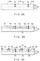
- Figs. 8A to 8E are sectional views in the manufacturing sequence of a semiconductor device according to an eighth embodiment of the present invention.
- a silicon body 20 having portions of different surface orientations, almost flush with each other, is formed by the method explained referring to Figs. 3A to 3E (Fig. 8A).
- a photoresist (not shown) as a mask
- p-type impurities are introduced into the substrate 10 and epitaxial silicon layer 52 to form p-type wells 221 and 223 in the substrate 10 and a p-type well 222 in the epitaxial silicon layer 52.
- n-type impurities are introduced into the substrate 10 and epitaxial silicon layer 52 to form an n-type well 241 in the substrate 10 and a p-type well 242 in the epitaxial silicon layer 52 (Fig. 8B).
- a field oxide film 60 serving as an element separating region is formed on the substrate 10 and epitaxial silicon layer 52 by LOCOS techniques (Fig. 8C).
- a silicon nitride film 50 with a film thickness of W which insulates the substrate 10 from the epitaxial silicon layer 52. For this reason, it is not necessary to introduce the field oxide film 60 to this region.
- the silicon-exposed surfaces of the substrate 10 and epitaxial silicon layer 52 undergo, for example, thermal oxidation to form gate oxide films 62 (100) and 62 (110) (Fig. 8D).
- Fig. 5D there is the relationship between the thickness T OX(100) of the oxide film 62 (100) on the substrate with the (100) surface orientation and the thickness T OX(110) of the oxide film 62 (110) on the epitaxial silicon layer 52 with the (110) surface orientation, as represented by expression (1).
- an NMOS 26 (100) is formed in each of the p-type wells 221 and 223, an NMOS 26 (110) in the p-type well 222, a PMOS 28 (100) in the n-type well 241, and a PMOS 28 (110) in the n-type well 242. This completes the semiconductor device of the eighth embodiment (Fig. 8E).
- an NMOS and a PMOS may be formed in the portions of different surface orientations, respectively.
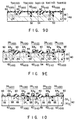
- Figs. 9A to 9E are sectional views in the manufacturing sequence of a semiconductor device according to a ninth embodiment of the present invention.
- n-type impurities are introduced into the n-type epitaxial silicon layer 54 to form a p-type well 22. Then, by using a new photoresist (not shown) as a mask, n-type impurities are introduced into the p-type substrate 30 to form an n-type well 24 (Fig. 9B).
- a field oxide film 60 serving as an element separating region is formed on the p-type substrate 30 and n-type epitaxial silicon layer 54 by LOCOS techniques (Fig. 9C). Since a silicon nitride film 50 with a film thickness of W is formed between the p-type substrate 30 and epitaxial silicon layer 54, it is not necessary to introduce the field oxide film 60 to this particular portion, as explained in Fig. 8C.
- the silicon-exposed surfaces of the p-type substrate 30 and n-type epitaxial silicon layer 54 undergo, for example, thermal oxidation to form gate oxide films 62 (100) and 62 (110) (Fig. 9D).
- Fig. 5D there is the relationship between the thickness T OX(100) of the oxide film 62 (100) and the thickness T OX(110) of the oxide film 62 (110) , as represented by expression (1).
- an NMOS 26 (100) is formed in the p-type substrate 30, an NMOS 26 (110) in the p-type well 22, a PMOS 28 (100) in the n-type well 24, and a PMOS 28 (110) in the n-type epitaxial silicon layer 54. This completes the semiconductor device of the ninth embodiment (Fig. 9E).
- an NMOS and a PMOS may be formed in the portions of different conductivity types, respectively.
- Fig. 10 is a sectional view of a semiconductor device according to a tenth embodiment of the present invention.
- a p-type silicon substrate 301 may be laminated to a p-type silicon substrate 302, and then a p-type epitaxial silicon layer 56 be grown on the substrate 302 to form a silicon body 42 of the p-type conductivity with different surface orientation portions almost flush with each other, and finally an NMOS 26 (100) , an NMOS 26 (110) , a PMOS 28 (100) , and a PMOS 28 (110) be formed in the resulting body.
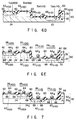
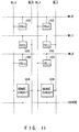
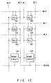
- Fig. 11 is a typical block diagram of a memory cell portion of a dynamic RAM (hereinafter, referred to as the DRAM), and Fig. 12 is a typical block diagram of a memory cell portion of a static RAM (hereinafter, referred to as the SRAM).
- DRAM dynamic RAM
- SRAM static RAM
- dynamic memory cells 100 or static memory cells 102 are connected at the intersections of word lines WL0 to WL3 and bit lines BL0, BL0 ⁇ (the symbol - means that the inverted signal is supplied), and BL1, BL1 ⁇ .
- the bit line pairs BL0, BL0 ⁇ and BL1, BL1 ⁇ of the DRAM and SRAM are generally connected to a sense circuit 104 that performs differential amplification of the data signal flowing through the bit line pair.
- Fig. 13 is a diagram showing a practical circuit con figuration of the sense circuit 104 shown in Figs. 11 and 12.
- the drain of PMOS 106 and that of NMOS 108 are connected to bit line BL0, one part of the bit line pair, to which the gate of PMOS 110 and that of NMOS 112 are also connected.
- the drain of PMOS 110 and that of NMOS 112 are connected to bit line BL0 ⁇ , the other part of the bit line pair, to which the gate of PMOS 106 and that of NMOS 108 are also connected.
- the sources of PMOSes 106 and 110 are each connected to a high-potential power supply VCC.
- NMOSes 108 and 112 are connected to a low-potential power supply, for example, the ground GND, via the current path of an NMOS 114 that, receiving the sense signal SENSE at its gate, switches the sense circuit 104.
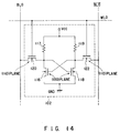
- Fig. 14 is a diagram showing a first practical circuit configuration of the static memory cell 102 shown in Fig. 12.
- the drain of NMOS 116 is connected to a high-potential power supply VCC via a resistance 117, as well as to the gate of NMOS 118.
- the source of NMOS 116 is connected to a low-potential power supply, for example, the ground GND.
- the drain of NMOS 118 is connected to the high-potential power supply VCC via a resistance 119, and its source is connected to the ground GND and the gate of NMOS 116.
- These NMOSes 116 and 118, resistances 117 and 119 constitute a latch circuit, which latches the data for subsequent use.
- the drain of NMOS 116 is connected to bit line BL0 via the current path of a data transfer transistor NMOS 120.
- the drain of NMOS 118 is connected to bit line BL0 ⁇ via the current path of a data transfer transistor NMOS 122.
- the gate of each of NMOSes 120 and 122 is connected to word line WL.
- NMOSes 120 and 122 are made up of NMOS 26 (110) , which provides a thicker gate oxide film, while NMOSes 116 and 118 (data-driving transistors) are composed of NMOS 26 (100) , which provides a thinner gate oxide film.
- NMOSes 116 and 118 data-driving transistors
- NMOS 26 100
- a difference in the gate oxide film thickness creates a difference in the driving capability of MOSFET, thereby increasing the ratio ⁇ T / ⁇ D .
- Fig. 15 is a diagram showing a second practical circuit configuration of the static memory cell 102 shown in Fig. 12.
- NMOSes 116 and 118, and PMOSes 121 and 123 constitute a latch circuit, which latches the data for subsequent use.
- NMOSes 116 and 118, and PMOSes 121 and 123 are formed in different surface orientation portions, respectively.
- the NMOS formation region (such as the p-type well 22 or p-type silicon substrate 30) is separated from the PMOS formation region (such as the n-type well 24 or n-type epitaxial layer 54) by silicon nitride film 50. That is, using the nitride film 50 as the element-separating region makes the size of the region smaller than that formed by, for example, LOCOS techniques, thereby reducing the cell area. This provides a device construction suitable for a high-capacity static RAM, for example.
- the effect of making the element separating region finer can be obtained with not only the static memory cell but also devices of other CMOS circuit arrangements.
- the silicon nitride film 50 separates elements of the same conductivity type from each other, such as NMOS on the (100) plane from NMOS on the (110) plane, or PMOS on the (100) plane from PMOS on the (110) plane, in addition to separating the elements, such as NMOS and PMOS, of the CMOS circuit.
- NMOSes 116 and 118 are composed of NMOS 26 (100)
- PMOSes 121 and 123 are made up of PMOS 28 (110) .
- NMOSes 120 and 122 are made up of NMOS 26 (110) , which provides a thicker gate oxide film, taking into account the cell stability.
- Fig. 16 is a typical block diagram of a memory cell portion and a row decoder portion of a programmable ROM (hereinafter, referred to as the PROM).
- PROM programmable ROM
- PROMs include EPROMs, which electrically write the data and erase it by radiation of ultraviolet rays, and EEPROMs, which electrically write and erase the data.
- level shifters 134 are provided between the outputs of AND gates 133 constituting the row decoder 132 and word lines WL0 to WL3 in order to raise the potential of word lines WL0 to WL3 for activation.
- Fig. 17 is a diagram showing a practical circuit con figuration of the AND gate 133 and level shifter 134 of Fig. 16.
- the AND gate 133 is constructed in such a manner that the source and drain of PMOS 140 are connected to the source and drain of PMOS 142, respectively, and a NAND gate composed of NMOSes 144 and 146 whose current paths are connected in series with each other is connected between the common drain and the low-potential power supply, for example, the ground GND, and then the output of the NAND gate is inverted by an inverter made up of PMOS 148 and NMOS 150.
- Address signal A0 is supplied to the gates of PMOS 142 and NMOS 146, and address signal A1 to the gates of PMOS 140 and NMOS 144.
- the level shifter 134 is composed as follows.
- the source of PMOS 152 is connected to the high-potential power supply VCC or a terminal Vsw to which a program potential VPP is selectively supplied, and its drain is connected to the drain of NMOS 154.
- PMOS 152 also has its gate connected to the drain of PMOS 156 as well as the drain of NMOS 158 and word line WL3.
- NMOS 154 has its source connected to the drains of PMOS 148 and NMOS 150 of the NAND gate 133, and its gate supplied with the high-potential power supply VCC.
- the gate of PMOS 156 is connected to the drains of PMOS 152 and NMOS 154.
- NMOS 158 has its gate connected to the source of NMOS 154, and its source connected to a low-potential power supply, for example, the ground GND.
- NMOS 158 With the level shifter 134 of the above arrangement, receiving a high level signal (VCC) from the NAND gate 133, NMOS 158 turns on. This causes PMOS 152 to turn on, bringing word line WL3 into the low level. Contrarily, receiving a low level signal from the NAND gate 133, NMOS 158 turns off. This causes NMOS 154 to turn on, which makes PMOS 156 turn on, bringing word line WL3 into the high level (VCC or VPP).
- VCC high level signal
- PMOSes 140, 142 and 148, and NMOSes 144, 146 and 150 constituting the row decoder 133 should be made up of MOSFETs of a fine construction. Making the MOSFET finer creates the problem of decreasing the breakdown voltage. Consequently, constructing the row decoder 133 and level shifter 134 of MOSFETs of the same configuration is expected to prevent the PROM from having a larger capacity.
- PMOSes 152 and 156, and NMOSes 154 and 158 are made up of NMOS 26 (110) and PMOS 28 (110) , which provides a thicker gate oxide film, and PMOSes 140, 142 and 148, NMOSes 144, 146 and 150 are composed of NMOS 26 (100) and PMOS 28 (100) with the thinner gate oxide film.
- This makes it possible to make the row decoder 133 of MOSFETs whose gate oxide film is thin enough for finer design, and to construct the level shifter 134 of MOSFETs whose thick gate oxide film provides a high breakdown voltage.
- Fig. 18 is a perspective view, in cross section, of a portion of the MOSFET constituting a memory cell portion and peripheral circuit portion of the PROM of Fig. 16.
- a first gate insulating film between the floating gate electrode 160 and p-type substrate 301 is made thin enough to become a tunnel insulating film.
- a memory cell 130 is formed on the p-type substrate 301 with the (100) surface orientation, and the MOSFETs (PMOS 26 (110) and NMOS 28 (110) ) constituting the peripheral circuit portions of the row decoder and others are formed on, for example, the p-type epitaxial silicon layer 56 with the (110) surface orientation.
- a gate insulting film can be formed so that the gate oxide film 62 (100) may differ from the gate oxide film 62 (110) in film thickness. This makes it possible to form a gate insulating film so thin that a tunnel phenomenon of electrons takes place at the memory cell 130, and at the peripheral circuit portion, to make a gate insulating film thick enough to prevent a tunnel phenomenon from occurring during the normal circuit operation.
- the silicon nitride film 50 which is formed so that the epitaxial silicon layers 52, 54, and 56 formed on the substrate 12 or 32 may be less affected by the crystal orientations of the substrate 10 or 30 during their growth, may be made up of other insulating films such as a silicon oxide film.
- the substrates 10 and 30 and that of the substrates 12 and 32 it is possible to reverse the surface orientation of the substrates 10 and 30 and that of the substrates 12 and 32, that is, to give the substrates 10 and 30 the (100) surface orientation, and the substrates 12 and 32 the (100) surface orientation.
- the surface orientation is not restricted to (100) and (110).
- Other surface orientations such as (111) may be used, taking into account the characteristics of an active element to be made, oxidation rate, and others.
- bipolar transistors in addition to MOSFFETs
- MOSFFETs MOSFFETs
- a bipolar transistor may be formed in each portion with the surface orientation assuring the optimum characteristics. This is also with the scope of the present invention.
Landscapes
- Metal-Oxide And Bipolar Metal-Oxide Semiconductor Integrated Circuits (AREA)
- Thin Film Transistor (AREA)
Applications Claiming Priority (3)
| Application Number | Priority Date | Filing Date | Title |
|---|---|---|---|
| JP253899/91 | 1991-10-01 | ||
| JP3253899A JP3017860B2 (ja) | 1991-10-01 | 1991-10-01 | 半導体基体およびその製造方法とその半導体基体を用いた半導体装置 |
| JP25389991 | 1991-10-01 |
Publications (3)
| Publication Number | Publication Date |
|---|---|
| EP0535681A2 true EP0535681A2 (de) | 1993-04-07 |
| EP0535681A3 EP0535681A3 (en) | 1996-01-17 |
| EP0535681B1 EP0535681B1 (de) | 1999-12-22 |
Family
ID=17257635
Family Applications (1)
| Application Number | Title | Priority Date | Filing Date |
|---|---|---|---|
| EP92116847A Expired - Lifetime EP0535681B1 (de) | 1991-10-01 | 1992-10-01 | Halbleiterkörper, Verfahren zu seiner Herstellung und Halbleiteranordnung mit diesem Körper |
Country Status (5)
| Country | Link |
|---|---|
| US (1) | US5384473A (de) |
| EP (1) | EP0535681B1 (de) |
| JP (1) | JP3017860B2 (de) |
| KR (1) | KR960008733B1 (de) |
| DE (1) | DE69230458T2 (de) |
Cited By (7)
| Publication number | Priority date | Publication date | Assignee | Title |
|---|---|---|---|---|
| US6518628B1 (en) | 1997-05-15 | 2003-02-11 | Siemens Aktiengesellschaft | Integrated CMOS circuit configuration, and production of same |
| WO2004114400A1 (en) | 2003-06-17 | 2004-12-29 | International Business Machines Corporation | High-performance cmos soi device on hybrid crystal-oriented substrates |
| WO2006096380A1 (en) * | 2005-03-07 | 2006-09-14 | Advanced Micro Devices, Inc. | Integrated circuit and method for its manufacture |
| WO2006132711A1 (en) * | 2005-06-07 | 2006-12-14 | Advanced Micro Devices, Inc. | Methods for manufacturing integrated circuits |
| WO2005057631A3 (en) * | 2003-12-02 | 2007-05-10 | Ibm | Planar substrate with selected semiconductor crystal orientations formed by localized amorphzation and recrystallization of stacked template layers |
| EP1848039A2 (de) | 2001-12-13 | 2007-10-24 | OHMI, Tadahiro | Komplementäre MIS-Vorrichtung |
| US7547616B2 (en) | 2005-06-01 | 2009-06-16 | International Business Machines Corporation | Laser processing method for trench-edge-defect-free solid phase epitaxy in confined geometrics |
Families Citing this family (72)
| Publication number | Priority date | Publication date | Assignee | Title |
|---|---|---|---|---|
| JP2605597B2 (ja) * | 1993-09-09 | 1997-04-30 | 日本電気株式会社 | 半導体装置の製造方法 |
| US5698893A (en) * | 1995-01-03 | 1997-12-16 | Motorola, Inc. | Static-random-access memory cell with trench transistor and enhanced stability |
| US5994188A (en) * | 1996-04-15 | 1999-11-30 | Delco Electronics Corporation | Method of fabricating a vertical power device with integrated control circuitry |
| KR100223915B1 (ko) * | 1996-10-22 | 1999-10-15 | 구본준 | 반도체 소자의 구조 및 제조방법 |
| KR100344818B1 (ko) * | 1997-09-24 | 2002-11-18 | 주식회사 하이닉스반도체 | 반도체소자및그의제조방법 |
| JP4521542B2 (ja) * | 1999-03-30 | 2010-08-11 | ルネサスエレクトロニクス株式会社 | 半導体装置および半導体基板 |
| US6483171B1 (en) * | 1999-08-13 | 2002-11-19 | Micron Technology, Inc. | Vertical sub-micron CMOS transistors on (110), (111), (311), (511), and higher order surfaces of bulk, SOI and thin film structures and method of forming same |
| US6861326B2 (en) | 2001-11-21 | 2005-03-01 | Micron Technology, Inc. | Methods of forming semiconductor circuitry |
| US6967351B2 (en) * | 2001-12-04 | 2005-11-22 | International Business Machines Corporation | Finfet SRAM cell using low mobility plane for cell stability and method for forming |
| US20050013996A1 (en) * | 2002-03-08 | 2005-01-20 | Hatfield Stephen F. | Hot melt pressure sensitive adhesives for disposable articles |
| KR100450683B1 (ko) * | 2002-09-04 | 2004-10-01 | 삼성전자주식회사 | Soi 기판에 형성되는 에스램 디바이스 |
| US6902962B2 (en) * | 2003-04-04 | 2005-06-07 | Taiwan Semiconductor Manufacturing Company, Ltd. | Silicon-on-insulator chip with multiple crystal orientations |
| JP4700264B2 (ja) * | 2003-05-21 | 2011-06-15 | 財団法人国際科学振興財団 | 半導体装置 |
| US6821826B1 (en) * | 2003-09-30 | 2004-11-23 | International Business Machines Corporation | Three dimensional CMOS integrated circuits having device layers built on different crystal oriented wafers |
| CN100361302C (zh) * | 2003-10-29 | 2008-01-09 | 国际商业机器公司 | 混合衬底、集成半导体结构以及它们的制备方法 |
| US7319258B2 (en) * | 2003-10-31 | 2008-01-15 | Taiwan Semiconductor Manufacturing Company, Ltd. | Semiconductor-on-insulator chip with<100>-oriented transistors |
| US20050224797A1 (en) * | 2004-04-01 | 2005-10-13 | Taiwan Semiconductor Manufacturing Company, Ltd. | CMOS fabricated on different crystallographic orientation substrates |
| US7208815B2 (en) * | 2004-05-28 | 2007-04-24 | Taiwan Semiconductor Manufacturing Company, Ltd. | CMOS logic gate fabricated on hybrid crystal orientations and method of forming thereof |
| US7291886B2 (en) * | 2004-06-21 | 2007-11-06 | International Business Machines Corporation | Hybrid substrate technology for high-mobility planar and multiple-gate MOSFETs |
| DE102004031708B4 (de) * | 2004-06-30 | 2008-02-07 | Advanced Micro Devices, Inc., Sunnyvale | Verfahren zum Herstellen eines Substrats mit kristallinen Halbleitergebieten unterschiedlicher Eigenschaften |
| US7094634B2 (en) * | 2004-06-30 | 2006-08-22 | International Business Machines Corporation | Structure and method for manufacturing planar SOI substrate with multiple orientations |
| US7186622B2 (en) * | 2004-07-15 | 2007-03-06 | Infineon Technologies Ag | Formation of active area using semiconductor growth process without STI integration |
| JP2006040911A (ja) * | 2004-07-22 | 2006-02-09 | Renesas Technology Corp | 半導体装置及びその製造方法 |
| US7253034B2 (en) * | 2004-07-29 | 2007-08-07 | International Business Machines Corporation | Dual SIMOX hybrid orientation technology (HOT) substrates |
| US7348658B2 (en) * | 2004-08-30 | 2008-03-25 | International Business Machines Corporation | Multilayer silicon over insulator device |
| WO2006038305A1 (ja) * | 2004-10-01 | 2006-04-13 | Tadahiro Ohmi | 半導体装置およびその製造方法 |
| US7439542B2 (en) * | 2004-10-05 | 2008-10-21 | International Business Machines Corporation | Hybrid orientation CMOS with partial insulation process |
| CN100423265C (zh) * | 2004-10-15 | 2008-10-01 | 中国科学院上海微系统与信息技术研究所 | 三维互补金属氧化物半导体晶体管的制备方法 |
| DE102004057764B4 (de) * | 2004-11-30 | 2013-05-16 | Advanced Micro Devices, Inc. | Verfahren zur Herstellung eines Substrats mit kristallinen Halbleitergebieten mit unterschiedlichen Eigenschaften, die über einem kristallinen Vollsubstrat angeordnet sind und damit hergestelltes Halbleiterbauelement |
| DE102004064248B3 (de) * | 2004-11-30 | 2015-05-07 | Advanced Micro Devices, Inc. | Substrat mit kristallinen Halbleitergebieten mit unterschiedlichen Eigenschaften |
| DE102004060961B4 (de) * | 2004-12-17 | 2010-06-02 | Advanced Micro Devices, Inc., Sunnyvale | Verfahren zur Herstellung eines Hybridhalbleitersubstrats über einer vergrabenen Isolierschicht |
| US7298009B2 (en) * | 2005-02-01 | 2007-11-20 | Infineon Technologies Ag | Semiconductor method and device with mixed orientation substrate |
| US7268377B2 (en) * | 2005-02-25 | 2007-09-11 | International Business Machines Corporation | Structure and method of fabricating a hybrid substrate for high-performance hybrid-orientation silicon-on-insulator CMOS devices |
| US7288821B2 (en) * | 2005-04-08 | 2007-10-30 | International Business Machines Corporation | Structure and method of three dimensional hybrid orientation technology |
| US7605429B2 (en) * | 2005-04-15 | 2009-10-20 | International Business Machines Corporation | Hybrid crystal orientation CMOS structure for adaptive well biasing and for power and performance enhancement |
| JPWO2006114999A1 (ja) * | 2005-04-18 | 2008-12-18 | 国立大学法人京都大学 | 化合物半導体装置及び化合物半導体製造方法 |
| US7432149B2 (en) * | 2005-06-23 | 2008-10-07 | Taiwan Semiconductor Manufacturing Company, Ltd. | CMOS on SOI substrates with hybrid crystal orientations |
| US7611937B2 (en) * | 2005-06-24 | 2009-11-03 | Taiwan Semiconductor Manufacturing Company, Ltd. | High performance transistors with hybrid crystal orientations |
| US7382029B2 (en) * | 2005-07-29 | 2008-06-03 | International Business Machines Corporation | Method and apparatus for improving integrated circuit device performance using hybrid crystal orientations |
| US7250656B2 (en) * | 2005-08-19 | 2007-07-31 | International Business Machines Corporation | Hybrid-orientation technology buried n-well design |
| US7737532B2 (en) * | 2005-09-06 | 2010-06-15 | Taiwan Semiconductor Manufacturing Company, Ltd. | Hybrid Schottky source-drain CMOS for high mobility and low barrier |
| US7605447B2 (en) * | 2005-09-22 | 2009-10-20 | International Business Machines Corporation | Highly manufacturable SRAM cells in substrates with hybrid crystal orientation |
| JP2007134593A (ja) * | 2005-11-11 | 2007-05-31 | Fujio Masuoka | 半導体装置およびその製造方法 |
| US7288458B2 (en) * | 2005-12-14 | 2007-10-30 | Freescale Semiconductor, Inc. | SOI active layer with different surface orientation |
| US8530355B2 (en) * | 2005-12-23 | 2013-09-10 | Infineon Technologies Ag | Mixed orientation semiconductor device and method |
| US20070145367A1 (en) * | 2005-12-27 | 2007-06-28 | Taiwan Semiconductor Manufacturing Company, Ltd. | Three-dimensional integrated circuit structure |
| US7754560B2 (en) | 2006-01-10 | 2010-07-13 | Freescale Semiconductor, Inc. | Integrated circuit using FinFETs and having a static random access memory (SRAM) |
| US7723805B2 (en) * | 2006-01-10 | 2010-05-25 | Freescale Semiconductor, Inc. | Electronic device including a fin-type transistor structure and a process for forming the electronic device |
| US7709303B2 (en) * | 2006-01-10 | 2010-05-04 | Freescale Semiconductor, Inc. | Process for forming an electronic device including a fin-type structure |
| US7414877B2 (en) * | 2006-01-23 | 2008-08-19 | Freescale Semiconductor, Inc. | Electronic device including a static-random-access memory cell and a process of forming the electronic device |
| US20070190795A1 (en) * | 2006-02-13 | 2007-08-16 | Haoren Zhuang | Method for fabricating a semiconductor device with a high-K dielectric |
| US7754587B2 (en) * | 2006-03-14 | 2010-07-13 | Freescale Semiconductor, Inc. | Silicon deposition over dual surface orientation substrates to promote uniform polishing |
| US7456055B2 (en) | 2006-03-15 | 2008-11-25 | Freescale Semiconductor, Inc. | Process for forming an electronic device including semiconductor fins |
| US7419866B2 (en) * | 2006-03-15 | 2008-09-02 | Freescale Semiconductor, Inc. | Process of forming an electronic device including a semiconductor island over an insulating layer |
| US7396407B2 (en) * | 2006-04-18 | 2008-07-08 | International Business Machines Corporation | Trench-edge-defect-free recrystallization by edge-angle-optimized solid phase epitaxy: method and applications to hybrid orientation substrates |
| JP4143096B2 (ja) | 2006-04-25 | 2008-09-03 | 株式会社東芝 | Mos型半導体装置及びその製造方法 |
| DE102006019835B4 (de) * | 2006-04-28 | 2011-05-12 | Advanced Micro Devices, Inc., Sunnyvale | Transistor mit einem Kanal mit Zugverformung, der entlang einer kristallographischen Orientierung mit erhöhter Ladungsträgerbeweglichkeit orientiert ist |
| WO2008005026A1 (en) * | 2006-07-07 | 2008-01-10 | International Business Machines Corporation | Method and apparatus for improving integrate circuit device performance using hydrid crystal orientations |
| US7595232B2 (en) * | 2006-09-07 | 2009-09-29 | International Business Machines Corporation | CMOS devices incorporating hybrid orientation technology (HOT) with embedded connectors |
| US7750406B2 (en) * | 2007-04-20 | 2010-07-06 | International Business Machines Corporation | Design structure incorporating a hybrid substrate |
| KR101461206B1 (ko) * | 2007-05-17 | 2014-11-12 | 가부시키가이샤 한도오따이 에네루기 켄큐쇼 | 반도체장치 및 그의 제조방법 |
| EP2065921A1 (de) | 2007-11-29 | 2009-06-03 | S.O.I.T.E.C. Silicon on Insulator Technologies | Verfahren zur Herstellung eines Halbleitersubstrats mit Bereichen verschiedener Kristallorientierung |
| US9059282B2 (en) | 2007-12-03 | 2015-06-16 | Infineon Technologies Ag | Semiconductor devices having transistors along different orientations |
| US8211786B2 (en) * | 2008-02-28 | 2012-07-03 | International Business Machines Corporation | CMOS structure including non-planar hybrid orientation substrate with planar gate electrodes and method for fabrication |
| FR2935539B1 (fr) * | 2008-08-26 | 2010-12-10 | Commissariat Energie Atomique | Circuit cmos tridimensionnel sur deux substrats desalignes et procede de realisation |
| TWI406362B (zh) * | 2009-11-19 | 2013-08-21 | Univ Nat United | A complementary gold - oxygen - semi - crystal system method for increasing the mobility of holes in PMOS element region |
| US20120080777A1 (en) * | 2010-09-30 | 2012-04-05 | Toshiba America Electronic Components, Inc. | Triple oxidation on dsb substrate |
| US8815699B2 (en) * | 2012-11-07 | 2014-08-26 | Globalfoundries Inc. | Fabrication of reverse shallow trench isolation structures with super-steep retrograde wells |
| US10062693B2 (en) * | 2016-02-24 | 2018-08-28 | International Business Machines Corporation | Patterned gate dielectrics for III-V-based CMOS circuits |
| US10593600B2 (en) | 2016-02-24 | 2020-03-17 | International Business Machines Corporation | Distinct gate stacks for III-V-based CMOS circuits comprising a channel cap |
| US9871050B1 (en) * | 2016-08-10 | 2018-01-16 | Globalfoundries Inc. | Flash memory device |
| US12176348B2 (en) | 2021-11-30 | 2024-12-24 | International Business Machines Corporation | Self-aligned hybrid substrate stacked gate-all-around transistors |
Family Cites Families (9)
| Publication number | Priority date | Publication date | Assignee | Title |
|---|---|---|---|---|
| US3476991A (en) * | 1967-11-08 | 1969-11-04 | Texas Instruments Inc | Inversion layer field effect device with azimuthally dependent carrier mobility |
| US3612960A (en) * | 1968-10-15 | 1971-10-12 | Tokyo Shibaura Electric Co | Semiconductor device |
| US3634737A (en) * | 1969-02-07 | 1972-01-11 | Tokyo Shibaura Electric Co | Semiconductor device |
| US3603848A (en) * | 1969-02-27 | 1971-09-07 | Tokyo Shibaura Electric Co | Complementary field-effect-type semiconductor device |
| JPS60154548A (ja) * | 1984-01-24 | 1985-08-14 | Fujitsu Ltd | 半導体装置の製造方法 |
| US4768076A (en) * | 1984-09-14 | 1988-08-30 | Hitachi, Ltd. | Recrystallized CMOS with different crystal planes |
| JPS6292361A (ja) * | 1985-10-17 | 1987-04-27 | Toshiba Corp | 相補型半導体装置 |
| JPS63228662A (ja) * | 1987-03-18 | 1988-09-22 | Toshiba Corp | 相補型mos半導体装置の製造方法 |
| JP2685819B2 (ja) * | 1988-03-31 | 1997-12-03 | 株式会社東芝 | 誘電体分離半導体基板とその製造方法 |
-
1991
- 1991-10-01 JP JP3253899A patent/JP3017860B2/ja not_active Expired - Lifetime
-
1992
- 1992-09-29 KR KR92017763A patent/KR960008733B1/ko not_active Expired - Fee Related
- 1992-09-30 US US07/953,808 patent/US5384473A/en not_active Expired - Lifetime
- 1992-10-01 EP EP92116847A patent/EP0535681B1/de not_active Expired - Lifetime
- 1992-10-01 DE DE69230458T patent/DE69230458T2/de not_active Expired - Lifetime
Cited By (13)
| Publication number | Priority date | Publication date | Assignee | Title |
|---|---|---|---|---|
| US6518628B1 (en) | 1997-05-15 | 2003-02-11 | Siemens Aktiengesellschaft | Integrated CMOS circuit configuration, and production of same |
| US7566936B2 (en) | 2001-12-13 | 2009-07-28 | Tokyo Electron Limited | Complementary MIS device |
| EP1848039A2 (de) | 2001-12-13 | 2007-10-24 | OHMI, Tadahiro | Komplementäre MIS-Vorrichtung |
| EP1848039A3 (de) * | 2001-12-13 | 2007-11-07 | OHMI, Tadahiro | Komplementäre MIS-Vorrichtung |
| EP1639637A1 (de) * | 2003-06-17 | 2006-03-29 | International Business Machines Corporation | Cmos soi bauelement auf hybriden kristallorientierten substraten mit hoher leistungsfähigkeit |
| WO2004114400A1 (en) | 2003-06-17 | 2004-12-29 | International Business Machines Corporation | High-performance cmos soi device on hybrid crystal-oriented substrates |
| US7713807B2 (en) | 2003-06-17 | 2010-05-11 | International Business Machines Corporation | High-performance CMOS SOI devices on hybrid crystal-oriented substrates |
| WO2005057631A3 (en) * | 2003-12-02 | 2007-05-10 | Ibm | Planar substrate with selected semiconductor crystal orientations formed by localized amorphzation and recrystallization of stacked template layers |
| US7785939B2 (en) | 2003-12-02 | 2010-08-31 | International Business Machines Corporation | Planar substrate with selected semiconductor crystal orientations formed by localized amorphization and recrystallization of stacked template layers |
| WO2006096380A1 (en) * | 2005-03-07 | 2006-09-14 | Advanced Micro Devices, Inc. | Integrated circuit and method for its manufacture |
| US7547616B2 (en) | 2005-06-01 | 2009-06-16 | International Business Machines Corporation | Laser processing method for trench-edge-defect-free solid phase epitaxy in confined geometrics |
| US7691733B2 (en) | 2005-06-01 | 2010-04-06 | International Business Machines Corporation | Laser processing method for trench-edge-defect-free solid phase epitaxy in confined geometrics |
| WO2006132711A1 (en) * | 2005-06-07 | 2006-12-14 | Advanced Micro Devices, Inc. | Methods for manufacturing integrated circuits |
Also Published As
| Publication number | Publication date |
|---|---|
| US5384473A (en) | 1995-01-24 |
| KR930009103A (ko) | 1993-05-22 |
| DE69230458D1 (de) | 2000-01-27 |
| EP0535681B1 (de) | 1999-12-22 |
| EP0535681A3 (en) | 1996-01-17 |
| DE69230458T2 (de) | 2000-07-13 |
| JPH0594928A (ja) | 1993-04-16 |
| KR960008733B1 (en) | 1996-06-29 |
| JP3017860B2 (ja) | 2000-03-13 |
Similar Documents
| Publication | Publication Date | Title |
|---|---|---|
| US5384473A (en) | Semiconductor body having element formation surfaces with different orientations | |
| US6998722B2 (en) | Semiconductor latches and SRAM devices | |
| KR100724029B1 (ko) | 반도체 장치 및 트랜지스터 | |
| US5960265A (en) | Method of making EEPROM having coplanar on-insulator FET and control gate | |
| US5635731A (en) | SRAM cell with no PN junction between driver and load transistors and method of manufacturing the same | |
| US8174058B2 (en) | Integrated circuits with split gate and common gate FinFET transistors | |
| US7099192B2 (en) | Nonvolatile flash memory and method of operating the same | |
| US5422499A (en) | Sixteen megabit static random access memory (SRAM) cell | |
| US4527255A (en) | Non-volatile static random-access memory cell | |
| JP3020199B2 (ja) | Sramセル及びその製造方法 | |
| JPH04162668A (ja) | 半導体装置およびその製造方法 | |
| US6512245B2 (en) | Semiconductor integrated circuit device | |
| US6849958B2 (en) | Semiconductor latches and SRAM devices | |
| TW200403838A (en) | Static semiconductor memory device | |
| US5920097A (en) | Compact, dual-transistor integrated circuit | |
| US6486007B2 (en) | Method of fabricating a memory cell for a static random access memory | |
| US4780751A (en) | Semiconductor integrated circuit device | |
| JP3039245B2 (ja) | 半導体メモリ装置 | |
| JP2005251776A (ja) | 半導体装置とその製造方法 | |
| JPH07302847A (ja) | Sramメモリセル | |
| JP3383428B2 (ja) | 半導体記憶装置 | |
| JP2853845B2 (ja) | 半導体装置およびその製造方法 | |
| JPS60161659A (ja) | 半導体集積回路装置 | |
| JP2594931B2 (ja) | 半導体記憶装置 | |
| JPH06188388A (ja) | 半導体記憶装置 |
Legal Events
| Date | Code | Title | Description |
|---|---|---|---|
| PUAI | Public reference made under article 153(3) epc to a published international application that has entered the european phase |
Free format text: ORIGINAL CODE: 0009012 |
|
| 17P | Request for examination filed |
Effective date: 19921001 |
|
| AK | Designated contracting states |
Kind code of ref document: A2 Designated state(s): DE FR GB |
|
| PUAL | Search report despatched |
Free format text: ORIGINAL CODE: 0009013 |
|
| AK | Designated contracting states |
Kind code of ref document: A3 Designated state(s): DE FR GB |
|
| 17Q | First examination report despatched |
Effective date: 19961014 |
|
| GRAG | Despatch of communication of intention to grant |
Free format text: ORIGINAL CODE: EPIDOS AGRA |
|
| GRAG | Despatch of communication of intention to grant |
Free format text: ORIGINAL CODE: EPIDOS AGRA |
|
| GRAH | Despatch of communication of intention to grant a patent |
Free format text: ORIGINAL CODE: EPIDOS IGRA |
|
| GRAH | Despatch of communication of intention to grant a patent |
Free format text: ORIGINAL CODE: EPIDOS IGRA |
|
| GRAA | (expected) grant |
Free format text: ORIGINAL CODE: 0009210 |
|
| AK | Designated contracting states |
Kind code of ref document: B1 Designated state(s): DE FR GB |
|
| PG25 | Lapsed in a contracting state [announced via postgrant information from national office to epo] |
Ref country code: FR Free format text: LAPSE BECAUSE OF FAILURE TO SUBMIT A TRANSLATION OF THE DESCRIPTION OR TO PAY THE FEE WITHIN THE PRESCRIBED TIME-LIMIT Effective date: 19991222 |
|
| REF | Corresponds to: |
Ref document number: 69230458 Country of ref document: DE Date of ref document: 20000127 |
|
| EN | Fr: translation not filed | ||
| PG25 | Lapsed in a contracting state [announced via postgrant information from national office to epo] |
Ref country code: GB Free format text: LAPSE BECAUSE OF NON-PAYMENT OF DUE FEES Effective date: 20001001 |
|
| PLBE | No opposition filed within time limit |
Free format text: ORIGINAL CODE: 0009261 |
|
| 26N | No opposition filed | ||
| GBPC | Gb: european patent ceased through non-payment of renewal fee |
Effective date: 20001001 |
|
| PGFP | Annual fee paid to national office [announced via postgrant information from national office to epo] |
Ref country code: DE Payment date: 20100929 Year of fee payment: 19 |
|
| REG | Reference to a national code |
Ref country code: DE Ref legal event code: R071 Ref document number: 69230458 Country of ref document: DE |
|
| REG | Reference to a national code |
Ref country code: DE Ref legal event code: R071 Ref document number: 69230458 Country of ref document: DE |