EP0540451A2 - Structure d'interconnexion à films minces et procédé associé - Google Patents
Structure d'interconnexion à films minces et procédé associé Download PDFInfo
- Publication number
- EP0540451A2 EP0540451A2 EP92480153A EP92480153A EP0540451A2 EP 0540451 A2 EP0540451 A2 EP 0540451A2 EP 92480153 A EP92480153 A EP 92480153A EP 92480153 A EP92480153 A EP 92480153A EP 0540451 A2 EP0540451 A2 EP 0540451A2
- Authority
- EP
- European Patent Office
- Prior art keywords
- metal
- polymer
- layer
- compensator
- via hole
- Prior art date
- Legal status (The legal status is an assumption and is not a legal conclusion. Google has not performed a legal analysis and makes no representation as to the accuracy of the status listed.)
- Withdrawn
Links
Images


Classifications
-
- H—ELECTRICITY
- H05—ELECTRIC TECHNIQUES NOT OTHERWISE PROVIDED FOR
- H05K—PRINTED CIRCUITS; CASINGS OR CONSTRUCTIONAL DETAILS OF ELECTRIC APPARATUS; MANUFACTURE OF ASSEMBLAGES OF ELECTRICAL COMPONENTS
- H05K3/00—Apparatus or processes for manufacturing printed circuits
- H05K3/44—Manufacturing insulated metal core circuits or other insulated electrically conductive core circuits
- H05K3/445—Manufacturing insulated metal core circuits or other insulated electrically conductive core circuits having insulated holes or insulated via connections through the metal core
-
- H—ELECTRICITY
- H05—ELECTRIC TECHNIQUES NOT OTHERWISE PROVIDED FOR
- H05K—PRINTED CIRCUITS; CASINGS OR CONSTRUCTIONAL DETAILS OF ELECTRIC APPARATUS; MANUFACTURE OF ASSEMBLAGES OF ELECTRICAL COMPONENTS
- H05K3/00—Apparatus or processes for manufacturing printed circuits
- H05K3/46—Manufacturing multilayer circuits
- H05K3/4611—Manufacturing multilayer circuits by laminating two or more circuit boards
- H05K3/4641—Manufacturing multilayer circuits by laminating two or more circuit boards having integrally laminated metal sheets or special power cores
-
- H—ELECTRICITY
- H10—SEMICONDUCTOR DEVICES; ELECTRIC SOLID-STATE DEVICES NOT OTHERWISE PROVIDED FOR
- H10W—GENERIC PACKAGES, INTERCONNECTIONS, CONNECTORS OR OTHER CONSTRUCTIONAL DETAILS OF DEVICES COVERED BY CLASS H10
- H10W70/00—Package substrates; Interposers; Redistribution layers [RDL]
- H10W70/01—Manufacture or treatment
- H10W70/05—Manufacture or treatment of insulating or insulated package substrates, or of interposers, or of redistribution layers
- H10W70/095—Manufacture or treatment of insulating or insulated package substrates, or of interposers, or of redistribution layers of vias therein
-
- H—ELECTRICITY
- H10—SEMICONDUCTOR DEVICES; ELECTRIC SOLID-STATE DEVICES NOT OTHERWISE PROVIDED FOR
- H10W—GENERIC PACKAGES, INTERCONNECTIONS, CONNECTORS OR OTHER CONSTRUCTIONAL DETAILS OF DEVICES COVERED BY CLASS H10
- H10W70/00—Package substrates; Interposers; Redistribution layers [RDL]
- H10W70/60—Insulating or insulated package substrates; Interposers; Redistribution layers
- H10W70/611—Insulating or insulated package substrates; Interposers; Redistribution layers for connecting multiple chips together
-
- H—ELECTRICITY
- H10—SEMICONDUCTOR DEVICES; ELECTRIC SOLID-STATE DEVICES NOT OTHERWISE PROVIDED FOR
- H10W—GENERIC PACKAGES, INTERCONNECTIONS, CONNECTORS OR OTHER CONSTRUCTIONAL DETAILS OF DEVICES COVERED BY CLASS H10
- H10W70/00—Package substrates; Interposers; Redistribution layers [RDL]
- H10W70/60—Insulating or insulated package substrates; Interposers; Redistribution layers
- H10W70/62—Insulating or insulated package substrates; Interposers; Redistribution layers characterised by their interconnections
- H10W70/63—Vias, e.g. via plugs
- H10W70/635—Through-vias
-
- H—ELECTRICITY
- H10—SEMICONDUCTOR DEVICES; ELECTRIC SOLID-STATE DEVICES NOT OTHERWISE PROVIDED FOR
- H10W—GENERIC PACKAGES, INTERCONNECTIONS, CONNECTORS OR OTHER CONSTRUCTIONAL DETAILS OF DEVICES COVERED BY CLASS H10
- H10W70/00—Package substrates; Interposers; Redistribution layers [RDL]
- H10W70/60—Insulating or insulated package substrates; Interposers; Redistribution layers
- H10W70/67—Insulating or insulated package substrates; Interposers; Redistribution layers characterised by their insulating layers or insulating parts
- H10W70/68—Shapes or dispositions thereof
- H10W70/685—Shapes or dispositions thereof comprising multiple insulating layers
-
- H—ELECTRICITY
- H05—ELECTRIC TECHNIQUES NOT OTHERWISE PROVIDED FOR
- H05K—PRINTED CIRCUITS; CASINGS OR CONSTRUCTIONAL DETAILS OF ELECTRIC APPARATUS; MANUFACTURE OF ASSEMBLAGES OF ELECTRICAL COMPONENTS
- H05K2201/00—Indexing scheme relating to printed circuits covered by H05K1/00
- H05K2201/01—Dielectrics
- H05K2201/0137—Materials
- H05K2201/0154—Polyimide
-
- H—ELECTRICITY
- H05—ELECTRIC TECHNIQUES NOT OTHERWISE PROVIDED FOR
- H05K—PRINTED CIRCUITS; CASINGS OR CONSTRUCTIONAL DETAILS OF ELECTRIC APPARATUS; MANUFACTURE OF ASSEMBLAGES OF ELECTRICAL COMPONENTS
- H05K2201/00—Indexing scheme relating to printed circuits covered by H05K1/00
- H05K2201/06—Thermal details
- H05K2201/068—Thermal details wherein the coefficient of thermal expansion is important
-
- H—ELECTRICITY
- H05—ELECTRIC TECHNIQUES NOT OTHERWISE PROVIDED FOR
- H05K—PRINTED CIRCUITS; CASINGS OR CONSTRUCTIONAL DETAILS OF ELECTRIC APPARATUS; MANUFACTURE OF ASSEMBLAGES OF ELECTRICAL COMPONENTS
- H05K2201/00—Indexing scheme relating to printed circuits covered by H05K1/00
- H05K2201/09—Shape and layout
- H05K2201/09209—Shape and layout details of conductors
- H05K2201/095—Conductive through-holes or vias
- H05K2201/09554—Via connected to metal substrate
-
- H—ELECTRICITY
- H05—ELECTRIC TECHNIQUES NOT OTHERWISE PROVIDED FOR
- H05K—PRINTED CIRCUITS; CASINGS OR CONSTRUCTIONAL DETAILS OF ELECTRIC APPARATUS; MANUFACTURE OF ASSEMBLAGES OF ELECTRICAL COMPONENTS
- H05K2201/00—Indexing scheme relating to printed circuits covered by H05K1/00
- H05K2201/09—Shape and layout
- H05K2201/09209—Shape and layout details of conductors
- H05K2201/095—Conductive through-holes or vias
- H05K2201/09563—Metal filled via
-
- H—ELECTRICITY
- H05—ELECTRIC TECHNIQUES NOT OTHERWISE PROVIDED FOR
- H05K—PRINTED CIRCUITS; CASINGS OR CONSTRUCTIONAL DETAILS OF ELECTRIC APPARATUS; MANUFACTURE OF ASSEMBLAGES OF ELECTRICAL COMPONENTS
- H05K2201/00—Indexing scheme relating to printed circuits covered by H05K1/00
- H05K2201/09—Shape and layout
- H05K2201/09209—Shape and layout details of conductors
- H05K2201/095—Conductive through-holes or vias
- H05K2201/096—Vertically aligned vias, holes or stacked vias
-
- H—ELECTRICITY
- H05—ELECTRIC TECHNIQUES NOT OTHERWISE PROVIDED FOR
- H05K—PRINTED CIRCUITS; CASINGS OR CONSTRUCTIONAL DETAILS OF ELECTRIC APPARATUS; MANUFACTURE OF ASSEMBLAGES OF ELECTRICAL COMPONENTS
- H05K2203/00—Indexing scheme relating to apparatus or processes for manufacturing printed circuits covered by H05K3/00
- H05K2203/01—Tools for processing; Objects used during processing
- H05K2203/0147—Carriers and holders
- H05K2203/0152—Temporary metallic carrier, e.g. for transferring material
-
- H—ELECTRICITY
- H05—ELECTRIC TECHNIQUES NOT OTHERWISE PROVIDED FOR
- H05K—PRINTED CIRCUITS; CASINGS OR CONSTRUCTIONAL DETAILS OF ELECTRIC APPARATUS; MANUFACTURE OF ASSEMBLAGES OF ELECTRICAL COMPONENTS
- H05K3/00—Apparatus or processes for manufacturing printed circuits
- H05K3/0011—Working of insulating substrates or insulating layers
- H05K3/0017—Etching of the substrate by chemical or physical means
- H05K3/0026—Etching of the substrate by chemical or physical means by laser ablation
- H05K3/0032—Etching of the substrate by chemical or physical means by laser ablation of organic insulating material
-
- H—ELECTRICITY
- H05—ELECTRIC TECHNIQUES NOT OTHERWISE PROVIDED FOR
- H05K—PRINTED CIRCUITS; CASINGS OR CONSTRUCTIONAL DETAILS OF ELECTRIC APPARATUS; MANUFACTURE OF ASSEMBLAGES OF ELECTRICAL COMPONENTS
- H05K3/00—Apparatus or processes for manufacturing printed circuits
- H05K3/0011—Working of insulating substrates or insulating layers
- H05K3/0017—Etching of the substrate by chemical or physical means
- H05K3/0026—Etching of the substrate by chemical or physical means by laser ablation
- H05K3/0032—Etching of the substrate by chemical or physical means by laser ablation of organic insulating material
- H05K3/0035—Etching of the substrate by chemical or physical means by laser ablation of organic insulating material of blind holes, i.e. having a metal layer at the bottom
-
- H—ELECTRICITY
- H05—ELECTRIC TECHNIQUES NOT OTHERWISE PROVIDED FOR
- H05K—PRINTED CIRCUITS; CASINGS OR CONSTRUCTIONAL DETAILS OF ELECTRIC APPARATUS; MANUFACTURE OF ASSEMBLAGES OF ELECTRICAL COMPONENTS
- H05K3/00—Apparatus or processes for manufacturing printed circuits
- H05K3/0058—Laminating printed circuit boards onto other substrates, e.g. metallic substrates
- H05K3/0061—Laminating printed circuit boards onto other substrates, e.g. metallic substrates onto a metallic substrate, e.g. a heat sink
-
- H—ELECTRICITY
- H05—ELECTRIC TECHNIQUES NOT OTHERWISE PROVIDED FOR
- H05K—PRINTED CIRCUITS; CASINGS OR CONSTRUCTIONAL DETAILS OF ELECTRIC APPARATUS; MANUFACTURE OF ASSEMBLAGES OF ELECTRICAL COMPONENTS
- H05K3/00—Apparatus or processes for manufacturing printed circuits
- H05K3/007—Manufacture or processing of a substrate for a printed circuit board supported by a temporary or sacrificial carrier
-
- H—ELECTRICITY
- H05—ELECTRIC TECHNIQUES NOT OTHERWISE PROVIDED FOR
- H05K—PRINTED CIRCUITS; CASINGS OR CONSTRUCTIONAL DETAILS OF ELECTRIC APPARATUS; MANUFACTURE OF ASSEMBLAGES OF ELECTRICAL COMPONENTS
- H05K3/00—Apparatus or processes for manufacturing printed circuits
- H05K3/38—Improvement of the adhesion between the insulating substrate and the metal
- H05K3/388—Improvement of the adhesion between the insulating substrate and the metal by the use of a metallic or inorganic thin film adhesion layer
-
- H—ELECTRICITY
- H05—ELECTRIC TECHNIQUES NOT OTHERWISE PROVIDED FOR
- H05K—PRINTED CIRCUITS; CASINGS OR CONSTRUCTIONAL DETAILS OF ELECTRIC APPARATUS; MANUFACTURE OF ASSEMBLAGES OF ELECTRICAL COMPONENTS
- H05K3/00—Apparatus or processes for manufacturing printed circuits
- H05K3/40—Forming printed elements for providing electric connections to or between printed circuits
- H05K3/4038—Through-connections; Vertical interconnect access [VIA] connections
- H05K3/4076—Through-connections; Vertical interconnect access [VIA] connections by thin-film techniques
-
- H—ELECTRICITY
- H05—ELECTRIC TECHNIQUES NOT OTHERWISE PROVIDED FOR
- H05K—PRINTED CIRCUITS; CASINGS OR CONSTRUCTIONAL DETAILS OF ELECTRIC APPARATUS; MANUFACTURE OF ASSEMBLAGES OF ELECTRICAL COMPONENTS
- H05K3/00—Apparatus or processes for manufacturing printed circuits
- H05K3/40—Forming printed elements for providing electric connections to or between printed circuits
- H05K3/42—Plated through-holes or plated via connections
- H05K3/423—Plated through-holes or plated via connections characterised by electroplating method
-
- H—ELECTRICITY
- H05—ELECTRIC TECHNIQUES NOT OTHERWISE PROVIDED FOR
- H05K—PRINTED CIRCUITS; CASINGS OR CONSTRUCTIONAL DETAILS OF ELECTRIC APPARATUS; MANUFACTURE OF ASSEMBLAGES OF ELECTRICAL COMPONENTS
- H05K3/00—Apparatus or processes for manufacturing printed circuits
- H05K3/46—Manufacturing multilayer circuits
- H05K3/4611—Manufacturing multilayer circuits by laminating two or more circuit boards
- H05K3/4614—Manufacturing multilayer circuits by laminating two or more circuit boards the electrical connections between the circuit boards being made during lamination
-
- H—ELECTRICITY
- H05—ELECTRIC TECHNIQUES NOT OTHERWISE PROVIDED FOR
- H05K—PRINTED CIRCUITS; CASINGS OR CONSTRUCTIONAL DETAILS OF ELECTRIC APPARATUS; MANUFACTURE OF ASSEMBLAGES OF ELECTRICAL COMPONENTS
- H05K3/00—Apparatus or processes for manufacturing printed circuits
- H05K3/46—Manufacturing multilayer circuits
- H05K3/4611—Manufacturing multilayer circuits by laminating two or more circuit boards
- H05K3/4614—Manufacturing multilayer circuits by laminating two or more circuit boards the electrical connections between the circuit boards being made during lamination
- H05K3/4617—Manufacturing multilayer circuits by laminating two or more circuit boards the electrical connections between the circuit boards being made during lamination characterized by laminating only or mainly similar single-sided circuit boards
-
- Y—GENERAL TAGGING OF NEW TECHNOLOGICAL DEVELOPMENTS; GENERAL TAGGING OF CROSS-SECTIONAL TECHNOLOGIES SPANNING OVER SEVERAL SECTIONS OF THE IPC; TECHNICAL SUBJECTS COVERED BY FORMER USPC CROSS-REFERENCE ART COLLECTIONS [XRACs] AND DIGESTS
- Y10—TECHNICAL SUBJECTS COVERED BY FORMER USPC
- Y10T—TECHNICAL SUBJECTS COVERED BY FORMER US CLASSIFICATION
- Y10T29/00—Metal working
- Y10T29/49—Method of mechanical manufacture
- Y10T29/49002—Electrical device making
- Y10T29/49117—Conductor or circuit manufacturing
- Y10T29/49124—On flat or curved insulated base, e.g., printed circuit, etc.
- Y10T29/49155—Manufacturing circuit on or in base
- Y10T29/49165—Manufacturing circuit on or in base by forming conductive walled aperture in base
-
- Y—GENERAL TAGGING OF NEW TECHNOLOGICAL DEVELOPMENTS; GENERAL TAGGING OF CROSS-SECTIONAL TECHNOLOGIES SPANNING OVER SEVERAL SECTIONS OF THE IPC; TECHNICAL SUBJECTS COVERED BY FORMER USPC CROSS-REFERENCE ART COLLECTIONS [XRACs] AND DIGESTS
- Y10—TECHNICAL SUBJECTS COVERED BY FORMER USPC
- Y10T—TECHNICAL SUBJECTS COVERED BY FORMER US CLASSIFICATION
- Y10T428/00—Stock material or miscellaneous articles
- Y10T428/12—All metal or with adjacent metals
- Y10T428/12361—All metal or with adjacent metals having aperture or cut
-
- Y—GENERAL TAGGING OF NEW TECHNOLOGICAL DEVELOPMENTS; GENERAL TAGGING OF CROSS-SECTIONAL TECHNOLOGIES SPANNING OVER SEVERAL SECTIONS OF THE IPC; TECHNICAL SUBJECTS COVERED BY FORMER USPC CROSS-REFERENCE ART COLLECTIONS [XRACs] AND DIGESTS
- Y10—TECHNICAL SUBJECTS COVERED BY FORMER USPC
- Y10T—TECHNICAL SUBJECTS COVERED BY FORMER US CLASSIFICATION
- Y10T428/00—Stock material or miscellaneous articles
- Y10T428/12—All metal or with adjacent metals
- Y10T428/12382—Defined configuration of both thickness and nonthickness surface or angle therebetween [e.g., rounded corners, etc.]
-
- Y—GENERAL TAGGING OF NEW TECHNOLOGICAL DEVELOPMENTS; GENERAL TAGGING OF CROSS-SECTIONAL TECHNOLOGIES SPANNING OVER SEVERAL SECTIONS OF THE IPC; TECHNICAL SUBJECTS COVERED BY FORMER USPC CROSS-REFERENCE ART COLLECTIONS [XRACs] AND DIGESTS
- Y10—TECHNICAL SUBJECTS COVERED BY FORMER USPC
- Y10T—TECHNICAL SUBJECTS COVERED BY FORMER US CLASSIFICATION
- Y10T428/00—Stock material or miscellaneous articles
- Y10T428/12—All metal or with adjacent metals
- Y10T428/12493—Composite; i.e., plural, adjacent, spatially distinct metal components [e.g., layers, joint, etc.]
- Y10T428/12535—Composite; i.e., plural, adjacent, spatially distinct metal components [e.g., layers, joint, etc.] with additional, spatially distinct nonmetal component
- Y10T428/12556—Organic component
-
- Y—GENERAL TAGGING OF NEW TECHNOLOGICAL DEVELOPMENTS; GENERAL TAGGING OF CROSS-SECTIONAL TECHNOLOGIES SPANNING OVER SEVERAL SECTIONS OF THE IPC; TECHNICAL SUBJECTS COVERED BY FORMER USPC CROSS-REFERENCE ART COLLECTIONS [XRACs] AND DIGESTS
- Y10—TECHNICAL SUBJECTS COVERED BY FORMER USPC
- Y10T—TECHNICAL SUBJECTS COVERED BY FORMER US CLASSIFICATION
- Y10T428/00—Stock material or miscellaneous articles
- Y10T428/12—All metal or with adjacent metals
- Y10T428/12493—Composite; i.e., plural, adjacent, spatially distinct metal components [e.g., layers, joint, etc.]
- Y10T428/12535—Composite; i.e., plural, adjacent, spatially distinct metal components [e.g., layers, joint, etc.] with additional, spatially distinct nonmetal component
- Y10T428/12556—Organic component
- Y10T428/12569—Synthetic resin
-
- Y—GENERAL TAGGING OF NEW TECHNOLOGICAL DEVELOPMENTS; GENERAL TAGGING OF CROSS-SECTIONAL TECHNOLOGIES SPANNING OVER SEVERAL SECTIONS OF THE IPC; TECHNICAL SUBJECTS COVERED BY FORMER USPC CROSS-REFERENCE ART COLLECTIONS [XRACs] AND DIGESTS
- Y10—TECHNICAL SUBJECTS COVERED BY FORMER USPC
- Y10T—TECHNICAL SUBJECTS COVERED BY FORMER US CLASSIFICATION
- Y10T428/00—Stock material or miscellaneous articles
- Y10T428/12—All metal or with adjacent metals
- Y10T428/12493—Composite; i.e., plural, adjacent, spatially distinct metal components [e.g., layers, joint, etc.]
- Y10T428/12771—Transition metal-base component
- Y10T428/12806—Refractory [Group IVB, VB, or VIB] metal-base component
-
- Y—GENERAL TAGGING OF NEW TECHNOLOGICAL DEVELOPMENTS; GENERAL TAGGING OF CROSS-SECTIONAL TECHNOLOGIES SPANNING OVER SEVERAL SECTIONS OF THE IPC; TECHNICAL SUBJECTS COVERED BY FORMER USPC CROSS-REFERENCE ART COLLECTIONS [XRACs] AND DIGESTS
- Y10—TECHNICAL SUBJECTS COVERED BY FORMER USPC
- Y10T—TECHNICAL SUBJECTS COVERED BY FORMER US CLASSIFICATION
- Y10T428/00—Stock material or miscellaneous articles
- Y10T428/12—All metal or with adjacent metals
- Y10T428/12493—Composite; i.e., plural, adjacent, spatially distinct metal components [e.g., layers, joint, etc.]
- Y10T428/12771—Transition metal-base component
- Y10T428/12806—Refractory [Group IVB, VB, or VIB] metal-base component
- Y10T428/12812—Diverse refractory group metal-base components: alternative to or next to each other
-
- Y—GENERAL TAGGING OF NEW TECHNOLOGICAL DEVELOPMENTS; GENERAL TAGGING OF CROSS-SECTIONAL TECHNOLOGIES SPANNING OVER SEVERAL SECTIONS OF THE IPC; TECHNICAL SUBJECTS COVERED BY FORMER USPC CROSS-REFERENCE ART COLLECTIONS [XRACs] AND DIGESTS
- Y10—TECHNICAL SUBJECTS COVERED BY FORMER USPC
- Y10T—TECHNICAL SUBJECTS COVERED BY FORMER US CLASSIFICATION
- Y10T428/00—Stock material or miscellaneous articles
- Y10T428/24—Structurally defined web or sheet [e.g., overall dimension, etc.]
- Y10T428/24777—Edge feature
-
- Y—GENERAL TAGGING OF NEW TECHNOLOGICAL DEVELOPMENTS; GENERAL TAGGING OF CROSS-SECTIONAL TECHNOLOGIES SPANNING OVER SEVERAL SECTIONS OF THE IPC; TECHNICAL SUBJECTS COVERED BY FORMER USPC CROSS-REFERENCE ART COLLECTIONS [XRACs] AND DIGESTS
- Y10—TECHNICAL SUBJECTS COVERED BY FORMER USPC
- Y10T—TECHNICAL SUBJECTS COVERED BY FORMER US CLASSIFICATION
- Y10T428/00—Stock material or miscellaneous articles
- Y10T428/31504—Composite [nonstructural laminate]
- Y10T428/31678—Of metal
-
- Y—GENERAL TAGGING OF NEW TECHNOLOGICAL DEVELOPMENTS; GENERAL TAGGING OF CROSS-SECTIONAL TECHNOLOGIES SPANNING OVER SEVERAL SECTIONS OF THE IPC; TECHNICAL SUBJECTS COVERED BY FORMER USPC CROSS-REFERENCE ART COLLECTIONS [XRACs] AND DIGESTS
- Y10—TECHNICAL SUBJECTS COVERED BY FORMER USPC
- Y10T—TECHNICAL SUBJECTS COVERED BY FORMER US CLASSIFICATION
- Y10T428/00—Stock material or miscellaneous articles
- Y10T428/31504—Composite [nonstructural laminate]
- Y10T428/31678—Of metal
- Y10T428/31681—Next to polyester, polyamide or polyimide [e.g., alkyd, glue, or nylon, etc.]
Definitions
- This invention relates generally to a structure and process for a thin film interconnect, and more particularly to a structure and process for multilayer thin film interconnect structures with improved dimensional stability and electrical performance.
- the invention further relates to a process of fabrication of the particular multilayer thin film structure, termed a "compensator", which functions as a ground plane (i.e., a reference plane).
- the compensator is comprised primarily of a metal sheet having a metallized via pattern and a high-temperature stable polymer as an insulator.
- Fabrication of multilayer thin film interconnect structures for high-density integrated circuits generally involves sequential build of metal-patterned dielectric layers on silicon or ceramic substrates.
- various dielectric/insulator materials which are generally used in the thin film structures, are sputtered or Plasma Enhanced Chemical Vapor Deposition (PECVD) quartz, silicon nitride, and high-temperature stable polymers, especially polyimides.
- PECVD Plasma Enhanced Chemical Vapor Deposition
- quartz silicon nitride
- high-temperature stable polymers especially polyimides.
- the most commonly used high-conductivity metallurgies are aluminum/copper, gold, and/or copper.
- an alternate approach to thin film interconnect structures is based on the assembly of individual electrically testable metallized thin films (layers) which are laminated at high temperature such that metal/metal and polymer/polymer bonding can be achieved.
- each metallized dielectric layer is fabricated as a single unit which can be fully tested for the desired electrical characteristics. Then each of these layers are stacked to form multiple layers and laminated under heat and pressure.
- a recent Japanese Patent Application No. 63-274199 (1988) entitled “Multilayer Wiring Formation Method” discloses individual build of layers, comprising polyimide insulator with copper wiring and copper/gold interface metal. This method is based on metal patterning of partially cured polyimide layers formed on a substrate, after which the layers are peeled off from the substrate, smoothed by vacuum, stacked, and then laminated in one step by heating under pressure. During this process, interlayer bonding occurs due to polymer interdiffusion at the interface which is also accompanied by full polymer cure, and at the same time gold/gold joining causes metal interconnections.
- the process according to this process would suffer the limitations of potential pattern misalignment/distortion mentioned above.
- U. S. - A. 2,692,190 issued to N. Pritikin (1954) discloses a method for generating embedded metallurgy to fabricate printed circuits having large dimensions on a temporary base plate which is removed by chemical etching every time. After the conductor pattern is defined, and an insulator such as Teflon, polystyrene etc., is applied, the base plate is removed by a selective etching process.
- an insulator such as Teflon, polystyrene etc.
- U. S. - A. 3,466,206 issued to J.T. Beck, (1969) also relates to a method of making embedded printed circuits, having integral aligned through terminals exposed on both sides by a subtractive etch process.
- the metal sheet can be copper, silver, gold, brass, stainless steel etc.
- the insulator is a thermosetting or cold-setting resin, self- hardening resin or one which requires heat and pressure for cure, including epoxies, phenolics, melamine, Teflon, or composites with glass fillers.
- One object of this invention is to provide a method for fabrication of a compensator for use in multilayer thin film structures to serve as a ground/reference plane for the signal wiring, and to provide dimensional stability to the structure.
- Another object is to provide a compensator with molybdenum or copper/Invar/copper as the metal core, high-temperature polyimide as the insulator, and aluminum, copper, gold, tungsten, or alloys thereof, as the via metallurgy.
- Another object is to provide a compensator with molybdenum or copper/Invar/copper as the metal core, high-temperature polyimide with low thermal coefficient of expansion (TCE) as the dielectric/insulator, and aluminum/copper, copper, tungsten, or gold as the via metallurgy.
- TCE thermal coefficient of expansion
- Another object is to provide a compensator for use in multilayer thin film structure such that the end device has improved electrical performance and dimensional stability.
- Hole filling with polymer is achieved by a special technique in two or three applications, with partial bake/cure between applications, and the final cure after the last top sided coating for a definite thickness.
- This process is not limited to any particular set of materials in terms of the metal type or polymer chemistry.
- One object of this invention is a new concept in fabricating a multilayer wiring structure, referred to as a "compensator", which is used as an integral part of thin film structure for enhancement of electrical performance and for providing dimensional stability of the thin film structure.
- Another object of this invention is to use the compensator in a multilayered structure.
- Still another object of this invention is a process of making the compensator comprising the steps of:
- this invention is a compensator interconnect structure used in forming a multilayer thin-film structure, said compensator comprising at least one metal layer, said metal layer having at least one opening, at least one layer of at least one polymer conformly coating said metal layer and lining said at least one opening, and wherein said opening has at least one via metal stud
- this invention is a process for the fabrication of a compensator interconnect used in forming a multilayer thin-film structure, said process comprising the steps of,
- this invention is a process for the fabrication of a compensator interconnect used in forming a multilayer thin-film structure, said process comprising the steps of,
- Figure 1 shows a thin metal foil that is used to form the metal core of the compensator of this invention.
- Figure 2 illustrates the metal core of the compensator after it has been etched from both sides to form two knife-edges in the via opening.
- Figure 3 shows the metal core of the compensator after the application of a thin layer of adhesion metal on both sides of the foil as well is in the via opening.
- Figure 4 shows a rigid support with a thermally stable polymer layer on the upper surface.
- Figure 5 shows the addition of a metal layer on top of the polymer layer from Figure 4.
- Figure 6 shows a partially cured second polymer layer on top of the metal layer from Figure 5.
- Figure 7 illustrates the lamination of the etched metal foil with the thin layer of adhesion metal of Figure 3, onto the partially cured polymer on the rigid support of Figure 6.
- Figure 8 shows the openings in the laminated structure of Figure 7 filled with a polymer.
- Figure 9 illustrates the structure of Figure 8, after planarization of the upper surface.
- Figure 10 shows etching of via holes within the planarized structure of Figure 9.
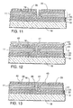
- Figure 11 illustrates a conformal coating of the planarized etched structure of Figure 10 with a metal seed layer.
- Figure 12 shows the conformal deposition of an electrically conductive metal over the metal seed layer and filling of the vias with an electrically conductive material.
- Figure 13 illustrates the structure of Figure 12 after planarization.
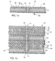
- Figure 14 shows the completed compensator after removal from the rigid support.
- Figure 15 illustrates the inclusion of completed compensators within a multilayer thin film interconnect structure.
- This invention describes an improved method of fabrication of multilayer interconnect structures and specifically a method of fabrication of a compensator which forms an integral part of the total thin film structure.
- the compensator serves as a ground/reference plane for the signal wiring, and provides improved electrical performance and dimensional stability.
- a single layer thin metal foil 11, is used to make the metal core of the compensator of this invention.
- the thin metal foil 11, could be made from a metal selected from a group comprising copper, molybdenum, titanium, tungsten, Invar, and alloys thereof. It is preferred that the thin metal foil 11, is approximately 35 micrometers (1.4 mil) to about 50 micrometers (2.0 mil) thick.
- the thin metal foil 11, could be a single layer foil comprising of a single material, or a multilayer foil comprising of a multilayered stacked material, or a single layer foil comprising of an alloyed material.
- Figure 2 illustrates the thin metal foil 11, after it has been etched from both sides to form two knife-edges 12, in the via opening 13, having via sidewalls 14.
- This double-sided etching of the thin metal foil 11, such as a molybdenum foil is done by etching techniques well-known in the art. See for example "Screening Masks and Method of Fabrication” I.B.M. Technical Disclosure Bulletin, Vol. 20, No. 2, pp. 577-578, (July 1977) the disclosure of which is incorporated herein by reference.
- the thin metal foil 11, itself is held in a holder (not shown), and care is taken that in this holder the thin metal foil 11, is not under too much tension or relaxation.
- a knife-edge 12, configuration is important for achieving uniform coverage of the via sidewalls 14, with an adhesion metal which is essential to metal/polymer adhesion durability during fabrication and accelerated testing, and for performance reliability of the electronic device.
- an adhesion metal which is essential to metal/polymer adhesion durability during fabrication and accelerated testing, and for performance reliability of the electronic device.
- TCE thermal coefficient of expansion
- Figure 3 shows the thin metal foil 11, used in compensator fabrication after the application of a thin layer of adhesion metal 16, on both sides of the metal foil 11, as well is in the via opening 13. This is also referred to as compensator core 17. Uniform coverage of the thin layer of adhesion metal 16, is done by sputter deposition, chemical vapor deposition (CVD), or electron-beam evaporation from both sides of the metal foil 11.
- the material for the thin layer of adhesion metal 16, could be selected from a group comprising chromium, copper, tantalum, titanium, or alloys thereof.
- a rigid support is needed. This is accomplished by taking a rigid support 18, and applying a first layer of polymer 19, over at least one of the surfaces. This is illustrated in Figure 4.
- the rigid support 18, could be a metal plate or a glass plate.
- a high-temperature stable polymer such as a polyimide
- This polymer is preferably a low thermal expansion (TCE) polyimide, such as the one derived from biphenic dianhydride - p-phenylene diamine (BPDA-PDA) and related materials.
- TCE thermal expansion
- BPDA-PDA biphenic dianhydride - p-phenylene diamine
- Low TCE polyimides including BPDA-PDA are described in E.P. Application n° 91480031.3.
- this polyimide can also be used to encapsulate the compensator core 17, and provide insulation between the via metallurgy and the metal via side-walls 14.
- Application n° 92480100.4 describes a high-density interconnect device and packaging structure having a low TCE polyimide insulator/dielectric and passivation layer and method of making such structures by sequential processing.
- the preferred low TCE polyimide is BPDA-PDA.
- the low TCE polyimides typically BPDA-PDA, provide matching thermal expansion with the molybdenum metal foil (both have TCEs about 5-6ppm/°C at 100 degrees C) and thus the composite structure has low interfacial residual stress and improved performance reliability. Thermal expansion mismatch is one of the major causes of high thermal stress in multilayer structures involving contacting materials of diverse characteristics.
- the low TCE polyimides have lower moisture uptake and lower dielectric constant than conventional polymers, and thus provide improved performance and long-term device performance reliability of the thin film interconnect structure comprising the laminated assembly of the individually fabricated layers including the compensator as one of the building blocks.
- the first polymer layer 19, of Figure 4 is then fully cured in a nitrogen-purged oven.
- the metal layer 20, serves as an etch or laser stop layer in the process by which the finished compensator is removed from the rigid support 18.
- the metal layer 20, optionally can also serve as the base metal for circuitization of one side of the finished compensator, such that it itself forms a wiring layer.
- a second layer of polymer 21, is applied on top of the metal layer 20. This is illustrated in Figure 6.
- the second polymer layer 21, is partially cured in a nitrogen-purged oven. This second polymer layer 21, is to remain as an integral part of the compensator and serves as an interlevel dielectric/insulator for the metallized structure
- the material for the polymer layers 19 and 21, can be selected from a group comprising polyimides in general, and, in the case of layer 21, preferably low TCE polyimides, aromatic polyesters, polyester-polyamides, and polyether-polyimides.
- Figure 7 illustrates the lamination of the compensator core 17, shown in Figure 3, having the thin layer of adhesion metal 16, to the second polymer layer 21, over the rigid support 18, as shown in Figure 6.
- This lamination is typically done by placing the compensator core 17, over the second polymer layer 21, such as a polyimide coating, and heating up to 150 degrees C at 2-3 degrees C/min ramp rate, while applying 50 psi pressure.
- the via openings 13, in the compensator core 17, are then filled with a polymer.
- a polymer 25 such as a polyimide.
- the polymer 25, should be of the same material as the partially cured second polymer layer 21, as shown in Figure 8, or it could be of a different material as long as it is compatible with the partially cured second polymer 21, that was applied on the surface of the rigid support 18.
- the polymer 25, is the same as polymer 21, and therefore they diffuse and form a single polymer 25.
- the via fill process according to this invention is such that it provides void-free polyimide-filled vias.
- FIG. 9 illustrates the structure after planarization, with the polyimide having a planarized surface 27.
- openings or etched via holes 33 and 34 are formed in the polymer or the polyimide 25, as shown in Figure 10. These openings or etched via holes 33 and 34, within the planarized structure are normally done by laser etching the via holes 33 and 34.
- the via hole or opening 33 must penetrate the entire thickness of the polymer 25, and the second polymer layer 21, and expose the upper surface of the metal layer 20.
- the via hole or opening 34 must penetrate the entire thickness of the polymer 25, and expose at least a portion of the upper surface of the thin layer of adhesion metal 16, covering the thin metal foil 11. Plasma ashing can then be done to remove ablation debris.
- metal seed layer 35 is typically selected from a group comprising chromium or copper or alloys thereof.
- the now well-defined via can be filled with an electrically conductive stud metal material 49, forming electrically conductive metal studs 41 and 42, as shown in Figure 12.
- the conductive stud metal material 49 could be of a different material than the metal seed layer 35, as shown in Figure 12, or it could also be of the same material.
- the preferred material for the conductive stud metal material 49 is selected from a group comprising aluminum, copper, gold, tungsten, and alloys thereof.
- the electrically conductive metal stud 41 can be formed in the opening by a variety of methods, for instance electroplating, sputtering, or evaporation, to name a few.
- the upper surface of the compensator is usually planarized, forming a planarized surface 43, as illustrated in Figure 13.
- Planarization of the surface removes the excess stud metal material 49, and the seed metal layer 35, from all areas other than the studs. This planarization process also insures that there will be a minimum number of defects, and that defects that may be formed on one level do not affect other levels or layers.
- the planarization method that is used should be such that the upper surfaces of the conductive metal studs 41 and 42, and the polymer layer 25, remain coplanar. Typically, such planarization is done by means of polishing techniques such as chem-mech polishing.
- the surfaces of the metallized vias are thickened by means of standard metallization processes, in order to form a raised "cap" which can aid in the subsequent joining of the individual layers of the thin film structure.
- the compensator 50 can now be removed from the rigid support 18. This can be accomplished in a number of ways, for example if the rigid support 18, is a glass plate or optically transparent material, then the removal can be carried by laser ablation of the bottom of the structure through the rigid support 18.
- FIG 14 shows the completed compensator 50, after removal from the rigid support 18, the first layer of polymer 19, and the metal layer 20.
- the rigid support 18, is removed by any of several methods known to those skilled in the art, for instance, by the use of a release layer or laser ablation as discussed earlier.
- the compensator 50 primarily comprises the compensator core material 17, as well as the insulator layers 21 and 25, the via metal studs 41 and 42, and the metal seed layer 35.
- the compensator 50 could also contain one or more blind vias 42.
- Figure 15 illustrates the use of completed compensators 50, in a multilayer thin film interconnect structure 75.
- the completed structure also contains electrically conductive X-signal line layer 53, electrically conductive Y-signal line layers 55, and a layer 57, which forms the top surface metallurgy layer.
- Vias 51 can be used to connect one wiring layer to another, such as X-wiring layer 53, to a Y-wiring layer 55.
- the compensator 50 insures that cross-talk between different wiring layers is reduced, if not fully eliminated.
- Vias 41 and 51 can be stacked during the process to connect the bottom surface metallurgy (not shown) to the top surface metallurgy shown in layer 57.
- the electrically conductive X-signal line layer 53 has at least one X-signal line 63, that may connect to one or more Y-signal line 65, through one or more through-via 61.
- a compensator 50′ is illustrated which is similar to the compensator 50, except it does not have the blind via 42.
- Double-sided etched molybdenum 35 micrometers (1.4 mil) thick with knife-edge vias is made according to molybdenum etch techniques using photoresists and masks which are well known in the art. See for example, "Screening Masks and Method of Fabrication” I.B.M. Technical Disclosure Bulletin, Vol. 20, No. 2, pp. 577-578, (July 1977).
- a thin layer (200-500A) of chromium is evaporated onto both sides of the etched molybdenum foil such that it not only forms a continuous film on the top and bottom surfaces, but also forms a conformal film on the via side-walls.
- a glass plate is coated on one side with 10 micrometers of polyimide which is fully cured.
- This polymer application is accomplished by means of spin, spray, or roller coating.
- a layer of chromium-copper-hromium metallurgy is then sputtered on top of this initial layer of polymer.
- the top and bottom cladding layer of chromium is preferably between 200 to 400 Angstrom thick and the copper layer is preferably 1 to 2 micrometers thick.
- a second layer (10 microns thick) of polymer is deposited on top of the metal layer. This polymer layer is then baked between 65 and 80 degrees Celsius for 60 minutes in a nitrogen-purged oven.
- the molybdenum foil having a chromium adhesion layer is laminated onto the polyimide by applying 50 psi pressure and heating up to 150 degrees Celsius at 2-3 degrees/minutes ramp rate, holding at 150 degrees Celsius for 30 minutes, and then cooling down to room temperature.
- polyimide precursor solution in a high-boiling solvent typically N-methylpyrrolidone (NMP)
- NMP N-methylpyrrolidone
- the polymer is allowed to permeate down and fill the holes, then doctor-bladed to squeeze out the excess from the surface region, and baked/cured at 80 degrees for 60 minutes and between 120 and 150 degrees for 60 minutes, and allowed to cool to room temperature.
- This polymer application process is repeated twice, with a bake between 120 and 150 degrees Celsius for 60 minutes between applications.
- a uniform layer of polymer is formed on the top by spin, spray, or roll coating, followed by bake/cure up to 400°C according to the following temperature cycle: 85°C for 60 minutes, 140°C for 60 minutes, 230°C for 60 minutes, 300°C for 45 minutes, and 350-400°C for 60 minutes.
- the via holes are laser ablated through the polymer, with a sidewall angle of 70-75 degrees.
- the part is then subjected to an oxygen plasma ash to remove ablation debris
- Metallization of the via holes is then done by sputter seed deposition of chromium/copper (200-400A chromium/0.3-1um copper), then electroplating of copper, followed by polishing until the desired level of planarization is achieved
- the compensator is then removed from the glass plate. This can be accomplished by laser ablation of the bottom of the structure through the glass plate.
- the bottom metal layer in the structure acts as a laser stop.
- the bottom polymer layer is removed by any technique known to one skilled in the art, e.g., oxygen plasma ashing.
- the bottom metal layer can then be removed by etching.
- this bottom metal layer can be patterned such that it itself forms a wiring layer, which can then become an integral part of the compensator.
- wiring layers can be formed on this compensator. Such layers can then be stacked/assembled such that the metal vias are aligned from layer to layer, and the individual layers are then laminated by applying heat and pressure.
- the thin film composite structure can then be laminated on top of a multilayer ceramic substrate to obtain a high-density packaging device.
- Advantages of individual build of metallized dielectric thin films are: greater throughput, lower cost, and the building blocks can be fully tested prior to assembly and lamination into the composite package, all of this allowing for fine-line wiring with reliable layer-to-layer alignment and high-density circuits.
Landscapes
- Engineering & Computer Science (AREA)
- Manufacturing & Machinery (AREA)
- Microelectronics & Electronic Packaging (AREA)
- Production Of Multi-Layered Print Wiring Board (AREA)
- Macromolecular Compounds Obtained By Forming Nitrogen-Containing Linkages In General (AREA)
- Insulated Metal Substrates For Printed Circuits (AREA)
- Internal Circuitry In Semiconductor Integrated Circuit Devices (AREA)
Applications Claiming Priority (2)
| Application Number | Priority Date | Filing Date | Title |
|---|---|---|---|
| US07/784,281 US5231751A (en) | 1991-10-29 | 1991-10-29 | Process for thin film interconnect |
| US784281 | 1997-01-15 |
Publications (2)
| Publication Number | Publication Date |
|---|---|
| EP0540451A2 true EP0540451A2 (fr) | 1993-05-05 |
| EP0540451A3 EP0540451A3 (en) | 1993-12-08 |
Family
ID=25131952
Family Applications (1)
| Application Number | Title | Priority Date | Filing Date |
|---|---|---|---|
| EP19920480153 Withdrawn EP0540451A3 (en) | 1991-10-29 | 1992-10-09 | Structure and process for thin film interconnect |
Country Status (3)
| Country | Link |
|---|---|
| US (3) | US5231751A (fr) |
| EP (1) | EP0540451A3 (fr) |
| JP (1) | JPH0821777B2 (fr) |
Cited By (2)
| Publication number | Priority date | Publication date | Assignee | Title |
|---|---|---|---|---|
| EP1065717A3 (fr) * | 1999-06-29 | 2003-08-20 | Sony Chemicals Corporation | Panneau à circuit à multi-couches |
| US7057279B2 (en) | 2001-11-26 | 2006-06-06 | Sony Corporation | High-frequency circuit block, its manufacturing method, high-frequency module device, and its manufacturing method |
Families Citing this family (107)
| Publication number | Priority date | Publication date | Assignee | Title |
|---|---|---|---|---|
| US5932289A (en) * | 1991-05-28 | 1999-08-03 | Trikon Technologies Limited | Method for filling substrate recesses using pressure and heat treatment |
| JPH06291216A (ja) * | 1993-04-05 | 1994-10-18 | Sony Corp | 基板及びセラミックパッケージ |
| JP3271094B2 (ja) * | 1993-07-05 | 2002-04-02 | ソニー株式会社 | 積層配線基板及びその製造方法 |
| US5373627A (en) * | 1993-11-23 | 1994-12-20 | Grebe; Kurt R. | Method of forming multi-chip module with high density interconnections |
| GB9401770D0 (en) * | 1994-01-31 | 1994-03-23 | Philips Electronics Uk Ltd | Manufacture of electronic devices comprising thin-film circuits |
| JP3290041B2 (ja) * | 1995-02-17 | 2002-06-10 | インターナショナル・ビジネス・マシーンズ・コーポレーション | 多層プリント基板、多層プリント基板の製造方法 |
| US5877551A (en) * | 1995-11-22 | 1999-03-02 | Olin Corporation | Semiconductor package having a ground or power ring and a metal substrate |
| US5872338A (en) | 1996-04-10 | 1999-02-16 | Prolinx Labs Corporation | Multilayer board having insulating isolation rings |
| US5830374A (en) * | 1996-09-05 | 1998-11-03 | International Business Machines Corporation | Method for producing multi-layer circuit board and resulting article of manufacture |
| JPH10163319A (ja) * | 1996-11-29 | 1998-06-19 | Hitachi Ltd | 半導体集積回路装置の製造方法 |
| US6075287A (en) * | 1997-04-03 | 2000-06-13 | International Business Machines Corporation | Integrated, multi-chip, thermally conductive packaging device and methodology |
| US6069068A (en) * | 1997-05-30 | 2000-05-30 | International Business Machines Corporation | Sub-quarter-micron copper interconnections with improved electromigration resistance and reduced defect sensitivity |
| US6130161A (en) | 1997-05-30 | 2000-10-10 | International Business Machines Corporation | Method of forming copper interconnections with enhanced electromigration resistance and reduced defect sensitivity |
| US6005198A (en) * | 1997-10-07 | 1999-12-21 | Dimensional Circuits Corporation | Wiring board constructions and methods of making same |
| FR2770339B1 (fr) * | 1997-10-27 | 2003-06-13 | Commissariat Energie Atomique | Structure munie de contacts electriques formes a travers le substrat de cette structure et procede d'obtention d'une telle structure |
| WO1999027579A1 (fr) * | 1997-11-26 | 1999-06-03 | Applied Materials, Inc. | Depot de revetement sculpte sans deterioration |
| US6140236A (en) * | 1998-04-21 | 2000-10-31 | Kabushiki Kaisha Toshiba | High throughput A1-Cu thin film sputtering process on small contact via for manufacturable beol wiring |
| TW420853B (en) * | 1998-07-10 | 2001-02-01 | Siemens Ag | Method of manufacturing the wiring with electric conducting interconnect between the over-side and the underside of the substrate and the wiring with such interconnect |
| US6461675B2 (en) * | 1998-07-10 | 2002-10-08 | Cvc Products, Inc. | Method for forming a copper film on a substrate |
| US6085415A (en) * | 1998-07-27 | 2000-07-11 | Ormet Corporation | Methods to produce insulated conductive through-features in core materials for electric packaging |
| US6190732B1 (en) | 1998-09-03 | 2001-02-20 | Cvc Products, Inc. | Method and system for dispensing process gas for fabricating a device on a substrate |
| US6274291B1 (en) | 1998-11-18 | 2001-08-14 | International Business Machines Corporation | Method of reducing defects in I/C card and resulting card |
| US6248958B1 (en) * | 1998-11-30 | 2001-06-19 | International Business Machines Corporation | Resistivity control of CIC material |
| US6965165B2 (en) * | 1998-12-21 | 2005-11-15 | Mou-Shiung Lin | Top layers of metal for high performance IC's |
| US6294836B1 (en) | 1998-12-22 | 2001-09-25 | Cvc Products Inc. | Semiconductor chip interconnect barrier material and fabrication method |
| US6036809A (en) * | 1999-02-16 | 2000-03-14 | International Business Machines Corporation | Process for releasing a thin-film structure from a substrate |
| US6468638B2 (en) | 1999-03-16 | 2002-10-22 | Alien Technology Corporation | Web process interconnect in electronic assemblies |
| US6245655B1 (en) | 1999-04-01 | 2001-06-12 | Cvc Products, Inc. | Method for planarized deposition of a material |
| JP2000349198A (ja) * | 1999-04-02 | 2000-12-15 | Nitto Denko Corp | チップサイズパッケージ用インターポーザ及びその製造方法と中間部材 |
| JP3592129B2 (ja) * | 1999-04-15 | 2004-11-24 | 新光電気工業株式会社 | 多層配線基板の製造方法 |
| US6492600B1 (en) * | 1999-06-28 | 2002-12-10 | International Business Machines Corporation | Laminate having plated microvia interconnects and method for forming the same |
| JP2001044589A (ja) * | 1999-07-30 | 2001-02-16 | Nitto Denko Corp | 回路基板 |
| JP3973340B2 (ja) * | 1999-10-05 | 2007-09-12 | Necエレクトロニクス株式会社 | 半導体装置、配線基板、及び、それらの製造方法 |
| JP2001185653A (ja) * | 1999-10-12 | 2001-07-06 | Fujitsu Ltd | 半導体装置及び基板の製造方法 |
| CN1199536C (zh) * | 1999-10-26 | 2005-04-27 | 伊比登株式会社 | 多层印刷配线板及多层印刷配线板的制造方法 |
| US6518509B1 (en) * | 1999-12-23 | 2003-02-11 | International Business Machines Corporation | Copper plated invar with acid preclean |
| US6560844B1 (en) * | 2000-02-24 | 2003-05-13 | Honeywell International Inc. | Alignment plate with matched thermal coefficient of expansion |
| US6627995B2 (en) | 2000-03-03 | 2003-09-30 | Cvc Products, Inc. | Microelectronic interconnect material with adhesion promotion layer and fabrication method |
| KR100509058B1 (ko) * | 2000-04-11 | 2005-08-18 | 엘지전자 주식회사 | 인쇄회로기판의 제조방법 |
| US6757176B1 (en) * | 2000-08-22 | 2004-06-29 | Micron Technology, Inc. | Circuit board |
| US6444263B1 (en) | 2000-09-15 | 2002-09-03 | Cvc Products, Inc. | Method of chemical-vapor deposition of a material |
| US6539625B2 (en) * | 2001-01-11 | 2003-04-01 | International Business Machines Corporation | Chromium adhesion layer for copper vias in low-k technology |
| JP2002252446A (ja) * | 2001-02-23 | 2002-09-06 | Sony Chem Corp | フレキシブル配線基板の製造方法 |
| US20020163062A1 (en) * | 2001-02-26 | 2002-11-07 | International Business Machines Corporation | Multiple material stacks with a stress relief layer between a metal structure and a passivation layer |
| US6879492B2 (en) * | 2001-03-28 | 2005-04-12 | International Business Machines Corporation | Hyperbga buildup laminate |
| US6617526B2 (en) * | 2001-04-23 | 2003-09-09 | Lockheed Martin Corporation | UHF ground interconnects |
| US6815709B2 (en) * | 2001-05-23 | 2004-11-09 | International Business Machines Corporation | Structure having flush circuitry features and method of making |
| US6606247B2 (en) | 2001-05-31 | 2003-08-12 | Alien Technology Corporation | Multi-feature-size electronic structures |
| JP4526747B2 (ja) * | 2001-08-17 | 2010-08-18 | 株式会社アドバンテスト | 配線基板の製造方法 |
| JP3967239B2 (ja) * | 2001-09-20 | 2007-08-29 | 株式会社フジクラ | 充填金属部付き部材の製造方法及び充填金属部付き部材 |
| US6691408B2 (en) * | 2001-10-10 | 2004-02-17 | Mack Technologies Florida, Inc. | Printed circuit board electrical interconnects |
| US6660945B2 (en) | 2001-10-16 | 2003-12-09 | International Business Machines Corporation | Interconnect structure and method of making same |
| JP3861669B2 (ja) * | 2001-11-22 | 2006-12-20 | ソニー株式会社 | マルチチップ回路モジュールの製造方法 |
| US7214569B2 (en) * | 2002-01-23 | 2007-05-08 | Alien Technology Corporation | Apparatus incorporating small-feature-size and large-feature-size components and method for making same |
| JP2003298232A (ja) | 2002-04-02 | 2003-10-17 | Sony Corp | 多層配線基板の製造方法および多層配線基板 |
| TW530377B (en) * | 2002-05-28 | 2003-05-01 | Via Tech Inc | Structure of laminated substrate with high integration and method of production thereof |
| JP2004039867A (ja) | 2002-07-03 | 2004-02-05 | Sony Corp | 多層配線回路モジュール及びその製造方法 |
| US20040148756A1 (en) * | 2002-09-09 | 2004-08-05 | Pommer Richard J. | Alignment plate with matched thermal coefficient of expansion |
| JP4057399B2 (ja) * | 2002-11-07 | 2008-03-05 | 株式会社フジクラ | 微細孔への金属充填方法 |
| JP4209178B2 (ja) * | 2002-11-26 | 2009-01-14 | 新光電気工業株式会社 | 電子部品実装構造及びその製造方法 |
| JP4059085B2 (ja) * | 2003-01-14 | 2008-03-12 | 松下電器産業株式会社 | 高周波積層部品およびその製造方法 |
| TWI239629B (en) * | 2003-03-17 | 2005-09-11 | Seiko Epson Corp | Method of manufacturing semiconductor device, semiconductor device, circuit substrate and electronic apparatus |
| US7253735B2 (en) | 2003-03-24 | 2007-08-07 | Alien Technology Corporation | RFID tags and processes for producing RFID tags |
| US7262075B2 (en) * | 2004-01-08 | 2007-08-28 | Georgia Tech Research Corp. | High-aspect-ratio metal-polymer composite structures for nano interconnects |
| DE102004025684B4 (de) | 2004-04-29 | 2024-08-22 | OSRAM Opto Semiconductors Gesellschaft mit beschränkter Haftung | Verfahren zum Ausbilden einer Kontaktstruktur zur elektrischen Kontaktierung eines optoelektronischen Halbleiterchips |
| JP4330486B2 (ja) * | 2004-05-07 | 2009-09-16 | 日東電工株式会社 | 両面プリント配線板の製造方法 |
| JP4670495B2 (ja) * | 2004-09-06 | 2011-04-13 | Tdk株式会社 | 電子デバイス及びその製造方法 |
| US7688206B2 (en) | 2004-11-22 | 2010-03-30 | Alien Technology Corporation | Radio frequency identification (RFID) tag for an item having a conductive layer included or attached |
| JP4564343B2 (ja) * | 2004-11-24 | 2010-10-20 | 大日本印刷株式会社 | 導電材充填スルーホール基板の製造方法 |
| JP4776247B2 (ja) * | 2005-02-09 | 2011-09-21 | 富士通株式会社 | 配線基板及びその製造方法 |
| JP2006231626A (ja) * | 2005-02-23 | 2006-09-07 | Fuji Photo Film Co Ltd | ノズルプレートの製造方法及び液体吐出ヘッド並びにこれを備えた画像形成装置 |
| US7615476B2 (en) * | 2005-06-30 | 2009-11-10 | Intel Corporation | Electromigration-resistant and compliant wire interconnects, nano-sized solder compositions, systems made thereof, and methods of assembling soldered packages |
| US7829793B2 (en) * | 2005-09-09 | 2010-11-09 | Magnecomp Corporation | Additive disk drive suspension manufacturing using tie layers for vias and product thereof |
| US8553364B1 (en) | 2005-09-09 | 2013-10-08 | Magnecomp Corporation | Low impedance, high bandwidth disk drive suspension circuit |
| KR100856326B1 (ko) * | 2006-07-19 | 2008-09-03 | 삼성전기주식회사 | 레이저 리프트 오프를 이용한 유전체 박막을 갖는 박막 커패시터 내장된 인쇄회로기판 제조방법, 및 이로부터 제조된 박막 커패시터 내장된 인쇄회로기판 |
| WO2008069260A1 (fr) * | 2006-11-30 | 2008-06-12 | Sanyo Electric Co., Ltd. | Carte de montage d'élément de circuit, composant de circuit utilisant celle-ci, et climatiseur |
| JP2008226989A (ja) * | 2007-03-09 | 2008-09-25 | Elpida Memory Inc | 半導体装置及び半導体装置の製造方法 |
| US8440916B2 (en) | 2007-06-28 | 2013-05-14 | Intel Corporation | Method of forming a substrate core structure using microvia laser drilling and conductive layer pre-patterning and substrate core structure formed according to the method |
| US8877565B2 (en) * | 2007-06-28 | 2014-11-04 | Intel Corporation | Method of forming a multilayer substrate core structure using sequential microvia laser drilling and substrate core structure formed according to the method |
| KR100969326B1 (ko) * | 2007-09-18 | 2010-07-09 | 삼성전기주식회사 | 다층 인쇄회로기판 및 그 제조방법 |
| TWI347810B (en) * | 2008-10-03 | 2011-08-21 | Po Ju Chou | A method for manufacturing a flexible pcb and the structure of the flexible pcb |
| KR100990546B1 (ko) | 2008-12-08 | 2010-10-29 | 삼성전기주식회사 | 비아 단부에 매립된 도금패턴을 갖는 인쇄회로기판 및 이의제조방법 |
| US8176628B1 (en) * | 2008-12-23 | 2012-05-15 | Amkor Technology, Inc. | Protruding post substrate package structure and method |
| KR101125567B1 (ko) * | 2009-12-24 | 2012-03-22 | 삼성모바일디스플레이주식회사 | 고분자 기판 및 그 제조 방법과 상기 고분자 기판을 포함하는 표시 장치 및 그 제조 방법 |
| JP5485714B2 (ja) * | 2010-01-07 | 2014-05-07 | セイコーインスツル株式会社 | パッケージの製造方法 |
| TWI461134B (zh) * | 2010-04-20 | 2014-11-11 | 南亞電路板股份有限公司 | 載板結構及其製作方法 |
| TWI436713B (zh) * | 2010-07-26 | 2014-05-01 | Via Tech Inc | 線路基板、線路基板製程 |
| TWI446842B (zh) * | 2012-06-18 | 2014-07-21 | 欣興電子股份有限公司 | 承載件及無核心封裝基板之製法 |
| JP2014086651A (ja) * | 2012-10-26 | 2014-05-12 | Ibiden Co Ltd | プリント配線板及びプリント配線板の製造方法 |
| JP6341714B2 (ja) * | 2014-03-25 | 2018-06-13 | 新光電気工業株式会社 | 配線基板及びその製造方法 |
| DE202014103821U1 (de) * | 2014-07-09 | 2014-09-09 | Carmen Diegel | Flexible elektrische Leiterstruktur |
| KR102326101B1 (ko) * | 2014-07-18 | 2021-11-12 | 미츠비시 가스 가가쿠 가부시키가이샤 | 적층체 및 반도체 소자 탑재용 기판, 그리고 그들의 제조 방법 |
| JP2016096297A (ja) * | 2014-11-17 | 2016-05-26 | イビデン株式会社 | 金属塊内蔵配線板及びその製造方法 |
| CN105931997B (zh) * | 2015-02-27 | 2019-02-05 | 胡迪群 | 暂时性复合式载板 |
| US9666514B2 (en) * | 2015-04-14 | 2017-05-30 | Invensas Corporation | High performance compliant substrate |
| TWI639573B (zh) * | 2015-09-02 | 2018-11-01 | 中聯資源股份有限公司 | 環保回塡材 |
| US10790426B2 (en) * | 2016-04-01 | 2020-09-29 | Nichia Corporation | Method of manufacturing light emitting element mounting base member, method of manufacturing light emitting device using the light emitting element mounting base member, light emitting element mounting base member, and light emitting device using the light emitting element mounting base member |
| EP3226290B1 (fr) | 2016-04-01 | 2024-04-17 | Nichia Corporation | Procédé de fabrication d'un élément de base de montage d'élément électroluminescent, et élément de base de montage d'élément électroluminescent |
| US9929203B1 (en) * | 2017-04-27 | 2018-03-27 | Taiwan Semiconductor Manufacturing Co., Ltd. | Semiconductor device and method for fabricating thereof |
| CN106952583B (zh) * | 2017-05-23 | 2019-04-30 | 深圳市华星光电技术有限公司 | 柔性阵列基板的制作方法 |
| JP7085328B2 (ja) * | 2017-09-29 | 2022-06-16 | 日東電工株式会社 | 配線回路基板、その製造方法および撮像装置 |
| JP2022505218A (ja) * | 2018-10-19 | 2022-01-14 | コーニング インコーポレイテッド | ビアを備えたデバイス並びにビアを製造するための方法および材料 |
| US11342256B2 (en) * | 2019-01-24 | 2022-05-24 | Applied Materials, Inc. | Method of fine redistribution interconnect formation for advanced packaging applications |
| JP7381323B2 (ja) * | 2019-12-17 | 2023-11-15 | 日東電工株式会社 | 両面配線回路基板の製造方法および両面配線回路基板 |
| CN111741592B (zh) * | 2020-06-17 | 2021-09-21 | 珠海越亚半导体股份有限公司 | 多层基板及其制作方法 |
| US12581979B2 (en) * | 2022-03-31 | 2026-03-17 | Beijing Boe Optoelectronics Technology Co., Ltd. | Substrate and preparation method thereof, integrated passive device, and electronic apparatus |
| CN118283947B (zh) * | 2024-03-12 | 2025-06-17 | 东南大学 | 一种玻璃通孔金属化的方法 |
Family Cites Families (25)
| Publication number | Priority date | Publication date | Assignee | Title |
|---|---|---|---|---|
| NL190034A (fr) * | 1953-08-17 | |||
| US2961746A (en) * | 1956-06-18 | 1960-11-29 | Aladdin Ind Inc | Printed circuits |
| US3181986A (en) * | 1961-03-31 | 1965-05-04 | Intellux Inc | Method of making inlaid circuits |
| US3466206A (en) * | 1962-06-01 | 1969-09-09 | Control Data Corp | Method of making embedded printed circuits |
| US3541222A (en) * | 1969-01-13 | 1970-11-17 | Bunker Ramo | Connector screen for interconnecting adjacent surfaces of laminar circuits and method of making |
| US4070501A (en) * | 1976-10-28 | 1978-01-24 | Ibm Corporation | Forming self-aligned via holes in thin film interconnection systems |
| JPS60147192A (ja) * | 1984-01-11 | 1985-08-03 | 株式会社日立製作所 | プリント配線板の製造方法 |
| DK291184D0 (da) * | 1984-06-13 | 1984-06-13 | Boeegh Petersen Allan | Fremgangsmaade og indretning til test af kredsloebsplader |
| JPS62108987A (ja) * | 1985-11-07 | 1987-05-20 | 三菱重工業株式会社 | 地熱ガス分離方法 |
| JPS62216287A (ja) * | 1986-03-17 | 1987-09-22 | 日本電解株式会社 | プリント回路用銅箔およびその製造方法 |
| JPH0654833B2 (ja) * | 1986-04-23 | 1994-07-20 | 日立化成工業株式会社 | 絶縁基板の製造方法 |
| JPH0191489A (ja) * | 1986-12-09 | 1989-04-11 | Matsushita Electric Works Ltd | 金属ベ−スプリント配線板 |
| JPS63224391A (ja) * | 1987-03-13 | 1988-09-19 | 株式会社アルメックス | スルホール用プリント配線板およびその製法 |
| US4963697A (en) * | 1988-02-12 | 1990-10-16 | Texas Instruments Incorporated | Advanced polymers on metal printed wiring board |
| US4995941A (en) * | 1989-05-15 | 1991-02-26 | Rogers Corporation | Method of manufacture interconnect device |
| US4933045A (en) * | 1989-06-02 | 1990-06-12 | International Business Machines Corporation | Thin film multilayer laminate interconnection board assembly method |
| FR2650471B1 (fr) * | 1989-07-27 | 1991-10-11 | Bull Sa | Procede de formation de piliers du reseau multicouche d'une carte de connexion d'au moins un circuit integre de haute densite |
| US5108819A (en) * | 1990-02-14 | 1992-04-28 | Eli Lilly And Company | Thin film electrical component |
| US5108562A (en) * | 1991-02-06 | 1992-04-28 | International Business Machines | Electrolytic method for forming vias and through holes in copper-invar-copper core structures |
| US5244538A (en) * | 1991-07-26 | 1993-09-14 | Microelectronics And Computer Technology Corporation | Method of patterning metal on a substrate using direct-write deposition of a mask |
| US5196251A (en) * | 1991-04-30 | 1993-03-23 | International Business Machines Corporation | Ceramic substrate having a protective coating thereon and a method for protecting a ceramic substrate |
| US5153986A (en) * | 1991-07-17 | 1992-10-13 | International Business Machines | Method for fabricating metal core layers for a multi-layer circuit board |
| US5209817A (en) * | 1991-08-22 | 1993-05-11 | International Business Machines Corporation | Selective plating method for forming integral via and wiring layers |
| US5326643A (en) * | 1991-10-07 | 1994-07-05 | International Business Machines Corporation | Adhesive layer in multi-level packaging and organic material as a metal diffusion barrier |
| US5232548A (en) * | 1991-10-29 | 1993-08-03 | International Business Machines Corporation | Discrete fabrication of multi-layer thin film, wiring structures |
-
1991
- 1991-10-29 US US07/784,281 patent/US5231751A/en not_active Expired - Fee Related
-
1992
- 1992-09-08 JP JP23916392A patent/JPH0821777B2/ja not_active Expired - Lifetime
- 1992-10-09 EP EP19920480153 patent/EP0540451A3/en not_active Withdrawn
-
1993
- 1993-01-21 US US08/006,414 patent/US6165629A/en not_active Expired - Fee Related
-
1999
- 1999-10-29 US US09/429,814 patent/US6228511B1/en not_active Expired - Fee Related
Cited By (2)
| Publication number | Priority date | Publication date | Assignee | Title |
|---|---|---|---|---|
| EP1065717A3 (fr) * | 1999-06-29 | 2003-08-20 | Sony Chemicals Corporation | Panneau à circuit à multi-couches |
| US7057279B2 (en) | 2001-11-26 | 2006-06-06 | Sony Corporation | High-frequency circuit block, its manufacturing method, high-frequency module device, and its manufacturing method |
Also Published As
| Publication number | Publication date |
|---|---|
| JPH05218603A (ja) | 1993-08-27 |
| JPH0821777B2 (ja) | 1996-03-04 |
| US5231751A (en) | 1993-08-03 |
| US6165629A (en) | 2000-12-26 |
| US6228511B1 (en) | 2001-05-08 |
| EP0540451A3 (en) | 1993-12-08 |
Similar Documents
| Publication | Publication Date | Title |
|---|---|---|
| US6165629A (en) | Structure for thin film interconnect | |
| US5224265A (en) | Fabrication of discrete thin film wiring structures | |
| US5199163A (en) | Metal transfer layers for parallel processing | |
| KR100263432B1 (ko) | 유기 칩 캐리어 및 그 제조 방법 | |
| US4783695A (en) | Multichip integrated circuit packaging configuration and method | |
| US5266446A (en) | Method of making a multilayer thin film structure | |
| US4918811A (en) | Multichip integrated circuit packaging method | |
| US4920639A (en) | Method of making a multilevel electrical airbridge interconnect | |
| EP0046525B1 (fr) | Structure planar métal-isolant à plusieurs niveaux comprenant un substrat, un réseau conductif d'interconnexion et une structure conductrice superposée et un procédé pour former une telle structure | |
| US5254493A (en) | Method of fabricating integrated resistors in high density substrates | |
| TWI734945B (zh) | 複合基板結構及其製作方法 | |
| US7420127B2 (en) | Method of manufacturing multilayer wiring substrate, and multilayer wiring substrate | |
| EP0450381B1 (fr) | Structure d'interconnexion multi-couche | |
| JPH0716094B2 (ja) | 配線板の製造法 | |
| JPH0923065A (ja) | 薄膜多層配線基板及びその製法 | |
| KR100720049B1 (ko) | 다층 배선판 및 그 제조 방법 | |
| EP0557278B1 (fr) | Procede de fabrication d'une structure de film mince multicouche | |
| JPH04277696A (ja) | 多層配線基板及びその製造方法 | |
| WO1991016725A1 (fr) | Procede de cablage de film mince multicouche se caracterisant par un auto-alignement des interconnexions entre couches | |
| US6711813B1 (en) | Method for fabricating a thin film build-up structure on a sequentially laminated printed circuit board base | |
| US6150074A (en) | Method of forming electrically conductive wiring pattern | |
| CN111315109B (zh) | 复合基板结构及其制作方法 | |
| US6074728A (en) | Multi-layered circuit substrate | |
| WO1990003100A1 (fr) | Cartes de circuits imprimes et procede pour la fabrication | |
| JP2565362B2 (ja) | 多層配線基板の製造方法 |
Legal Events
| Date | Code | Title | Description |
|---|---|---|---|
| PUAI | Public reference made under article 153(3) epc to a published international application that has entered the european phase |
Free format text: ORIGINAL CODE: 0009012 |
|
| AK | Designated contracting states |
Kind code of ref document: A2 Designated state(s): DE FR GB |
|
| 17P | Request for examination filed |
Effective date: 19930819 |
|
| PUAL | Search report despatched |
Free format text: ORIGINAL CODE: 0009013 |
|
| AK | Designated contracting states |
Kind code of ref document: A3 Designated state(s): DE FR GB |
|
| 17Q | First examination report despatched |
Effective date: 19950426 |
|
| 18D | Application deemed to be withdrawn |
Effective date: 19980501 |