EP0542267A2 - Korrekturschaltung für Bildabtaster - Google Patents
Korrekturschaltung für Bildabtaster Download PDFInfo
- Publication number
- EP0542267A2 EP0542267A2 EP92119373A EP92119373A EP0542267A2 EP 0542267 A2 EP0542267 A2 EP 0542267A2 EP 92119373 A EP92119373 A EP 92119373A EP 92119373 A EP92119373 A EP 92119373A EP 0542267 A2 EP0542267 A2 EP 0542267A2
- Authority
- EP
- European Patent Office
- Prior art keywords
- image scanner
- output
- photo detectors
- pixel
- density
- Prior art date
- Legal status (The legal status is an assumption and is not a legal conclusion. Google has not performed a legal analysis and makes no representation as to the accuracy of the status listed.)
- Granted
Links
Images


Classifications
-
- H—ELECTRICITY
- H04—ELECTRIC COMMUNICATION TECHNIQUE
- H04N—PICTORIAL COMMUNICATION, e.g. TELEVISION
- H04N25/00—Circuitry of solid-state image sensors [SSIS]; Control thereof
- H04N25/60—Noise processing, e.g. detecting, correcting, reducing or removing noise
- H04N25/67—Noise processing, e.g. detecting, correcting, reducing or removing noise applied to fixed-pattern noise, e.g. non-uniformity of response
- H04N25/671—Noise processing, e.g. detecting, correcting, reducing or removing noise applied to fixed-pattern noise, e.g. non-uniformity of response for non-uniformity detection or correction
- H04N25/672—Noise processing, e.g. detecting, correcting, reducing or removing noise applied to fixed-pattern noise, e.g. non-uniformity of response for non-uniformity detection or correction between adjacent sensors or output registers for reading a single image
-
- H—ELECTRICITY
- H04—ELECTRIC COMMUNICATION TECHNIQUE
- H04N—PICTORIAL COMMUNICATION, e.g. TELEVISION
- H04N25/00—Circuitry of solid-state image sensors [SSIS]; Control thereof
- H04N25/70—SSIS architectures; Circuits associated therewith
- H04N25/701—Line sensors
Definitions
- the present invention relates to an image scanner using CCDs.
- Fig. 5 schematically shows an ordinary CCD image sensor.
- S1, S2, ..., S N denote photo detectors
- OSR1, OSR2, ..., OSR N/2 denote odd-number-side shift registers for shifting out analog outputs of the photo detectors on the odd number side (photo detectors arranged in the odd number rows)
- ESR1, ESR2, ..., ESR N/2 denote the even-number-side shift registers for shifting out analog outputs of the photo detectors on the even number side (photo detectors arranges in the even number rows)
- OBUFF denotes an odd-number-side buffer amplifier
- EBUFF denotes an even-number-side buffer amplifier.
- SH denotes a start pulse for starting the shifting operation of the shift registers
- ⁇ 1 and ⁇ 2 denote transfer pulses
- ⁇ RE and ⁇ RO denote reset pulses
- O OUT denotes CCD output of the odd-number-side photo detectors
- E OUT denotes CCD output of the even-number-side photo detectors.
- the present invention has been made with the above problem in mind, and has as an object to provide an image scanner without variations in output.
- an image scanner comprising: an image sensor for individually issuing outputs of photo detectors arranged in odd number rows and outputs of photo detectors arranged in even number rows; and correcting means for correcting an issued output of a photo detector representing a density of a pixel of interest according to a level difference between said issued output and an issued output of at least one of adjacent photo detectors disposed on rows adjacent to a row on which said photo detector representing density of said pixel of interest is disposed.
- the image scanner includes means for correcting the output of the photo detector representing the density level of a pixel of interest according to a difference between this output of the photo detector representing the density level of the pixel of interest and an output of at least one of the adjacent photo detectors, and this image scanner provides effects that variations can be eliminated between the output of the odd-number-side photo detectors and the output of the even-number-side photo detectors, and that the edge of the image can be accentuated.
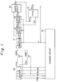
- Fig. 1 is a block diagram of the image scanner as an embodiment of the present invention.
- reference numeral 10 denotes a CCD image sensor shown in Fig. 5
- ASW1 and ASW2 denote analog switches for synthesizing CCD output of the odd-number-side photo detectors and CCD output of the even-number-side photo detectors.
- the analog switches ASW1 and ASW2 conduct a current respectively when the high level of transfer pulses ⁇ 1 and ⁇ 2 are applied thereto.
- Reference numeral 11 denotes an A/D converter which sequentially converts CCD output, received through the analog switches ASW1 and ASW2, into 8-bit digital signals CD1, CD2, ..., CD n-1 , CD n , CD n+1 at the leading edge of a timing clock signal T supplied from a control circuit 16.
- the 8-bit digital signals represent density levels of the pixels in a range of 0, 1, 2, ..., 255, in which 0 corresponds to the level of black, while 255 corresponds to the level of white.
- Reference numerals 12 and 13 denote latch circuits for latching output of the A/D converter 11 at the leading edge of a timing clock signal T.
- Fig. 2 shows waveforms of signals at various parts of the above-mentioned image scanner. Output D OUTn from ROM 15 can be expressed by the following equation.
- D OUTn CD n /(1-2 ⁇ ) - 2 ⁇
- AD n /(1-2 ⁇ ) CD n /(1-2 ⁇ ) - (CD n-1 + CD n+1 ) ⁇ /(1 - 2 ⁇ )
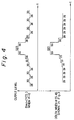
- the ⁇ is a function of an absolute value of a difference between CD n and AD n as shown in the graph in Fig. 3.
- the image when the difference between the density level of a pixel of interest, i. e. CD n and the density levels of the adjacent pixels, i. e. AD n is 2 or less, the image is blurred to the maximum degree. And, when the difference is in the range of 2 to 5, the image is blurred according to the degree of difference. When the difference is 7 or more, the edge of the image is accentuated to the maximum degree, and when the difference is in the range of 5 to 7, the edge of the image is accentuated according to the degree of the difference.
- ⁇ is the function of the difference between CD n and 1/2 (CD n-1 + CD n+1 ) , but ⁇ may be a function of the difference between CD n and CD n+1 (or CD n-1 ).
- Fig. 6 is a block diagram of another embodiment in which ⁇ is a function between CD n AND CD n+1 .
- the component elements whose function is the same as the component elements of the image scanner in Fig. 1 are designated by the same codes.
- composition of the image scanner of this embodiment differs from that of the image scanner in Fig. 1 in that subtracter circuits 20 and 23 are added and ROM 21 and ROM 22 are used in place of ROM 15.
- D OUT1n 2 ⁇ AD n /(1 - 2 ⁇ )
- D OUT2n CD n /(1 - 2 ⁇ )
- the image scanner in Fig. 6 can use a ROM with smaller capacity than the one in Fig. 1.
- ROM 15 in Fig. 1 must have 16 address terminals, but ROM 21 and ROM 22 in Fig. 6 need to have only 11 address terminals.
- various types of sensors other than the CCD type, such as one using a photodiode array, may be used.
Landscapes
- Engineering & Computer Science (AREA)
- Multimedia (AREA)
- Signal Processing (AREA)
- Facsimile Image Signal Circuits (AREA)
- Facsimile Scanning Arrangements (AREA)
- Solid State Image Pick-Up Elements (AREA)
- Transforming Light Signals Into Electric Signals (AREA)
- Facsimile Heads (AREA)
Applications Claiming Priority (4)
| Application Number | Priority Date | Filing Date | Title |
|---|---|---|---|
| JP29873291 | 1991-11-14 | ||
| JP298732/91 | 1991-11-14 | ||
| JP4294327A JP3037839B2 (ja) | 1991-11-14 | 1992-11-02 | イメージスキャナ |
| JP294327/92 | 1992-11-02 |
Publications (3)
| Publication Number | Publication Date |
|---|---|
| EP0542267A2 true EP0542267A2 (de) | 1993-05-19 |
| EP0542267A3 EP0542267A3 (en) | 1993-07-07 |
| EP0542267B1 EP0542267B1 (de) | 1995-07-26 |
Family
ID=26559778
Family Applications (1)
| Application Number | Title | Priority Date | Filing Date |
|---|---|---|---|
| EP92119373A Expired - Lifetime EP0542267B1 (de) | 1991-11-14 | 1992-11-12 | Korrekturschaltung für Bildabtaster |
Country Status (4)
| Country | Link |
|---|---|
| EP (1) | EP0542267B1 (de) |
| JP (1) | JP3037839B2 (de) |
| CA (1) | CA2082772C (de) |
| DE (1) | DE69203694T2 (de) |
Cited By (1)
| Publication number | Priority date | Publication date | Assignee | Title |
|---|---|---|---|---|
| EP0613289A1 (de) * | 1993-02-23 | 1994-08-31 | Sharp Kabushiki Kaisha | Bildleser |
Families Citing this family (1)
| Publication number | Priority date | Publication date | Assignee | Title |
|---|---|---|---|---|
| JPH11215298A (ja) * | 1998-01-22 | 1999-08-06 | Toshiba Corp | 画像情報処理装置と画像情報処理方法と画像形成装置 |
Family Cites Families (3)
| Publication number | Priority date | Publication date | Assignee | Title |
|---|---|---|---|---|
| US4541116A (en) * | 1984-02-27 | 1985-09-10 | Environmental Research Institute Of Mi | Neighborhood image processing stage for implementing filtering operations |
| US4860118A (en) * | 1987-02-25 | 1989-08-22 | Canon Kabushiki Kaisha | Image signal processing apparatus with edge emphasis and variable magnification |
| JPH02301295A (ja) * | 1989-05-15 | 1990-12-13 | Dainippon Printing Co Ltd | ビデオプリンタ装置 |
-
1992
- 1992-11-02 JP JP4294327A patent/JP3037839B2/ja not_active Expired - Fee Related
- 1992-11-12 CA CA002082772A patent/CA2082772C/en not_active Expired - Fee Related
- 1992-11-12 DE DE69203694T patent/DE69203694T2/de not_active Expired - Lifetime
- 1992-11-12 EP EP92119373A patent/EP0542267B1/de not_active Expired - Lifetime
Cited By (2)
| Publication number | Priority date | Publication date | Assignee | Title |
|---|---|---|---|---|
| EP0613289A1 (de) * | 1993-02-23 | 1994-08-31 | Sharp Kabushiki Kaisha | Bildleser |
| US5426291A (en) * | 1993-02-23 | 1995-06-20 | Sharp Kabushiki Kaisha | Reader with A/D conversion and high precise and high speed modes |
Also Published As
| Publication number | Publication date |
|---|---|
| JPH05211610A (ja) | 1993-08-20 |
| EP0542267A3 (en) | 1993-07-07 |
| CA2082772A1 (en) | 1993-05-15 |
| JP3037839B2 (ja) | 2000-05-08 |
| EP0542267B1 (de) | 1995-07-26 |
| DE69203694T2 (de) | 1996-03-21 |
| CA2082772C (en) | 1997-03-04 |
| DE69203694D1 (de) | 1995-08-31 |
Similar Documents
| Publication | Publication Date | Title |
|---|---|---|
| US5086343A (en) | Method and apparatus for compensating for sensitivity variations in the output of a solid state image sensor | |
| JPH0254683A (ja) | 画像走査装置およびその補正方法 | |
| US5838463A (en) | Binary image processor | |
| EP1137255B1 (de) | Korrekturverfahren und -vorrichtung für Bildsignale die durch einen Bildsensor mit mehreren Ausgangskanälen erzeugt wurden | |
| EP0710034B1 (de) | Vorrichtung und Verfahren zur Bildabtastung mit einer Sensoranordnung | |
| US5355164A (en) | Method and apparatus of correction image read signals by removing the influence of dark current therefrom | |
| EP0457522B1 (de) | Gammakorrekturschaltungen | |
| US5001768A (en) | Image reading apparatus | |
| US4954913A (en) | Image reading apparatus | |
| US6016370A (en) | Image data processing apparatus having pixel quantity conversion and error diffusion functions | |
| JPH09298647A (ja) | リニアイメージセンサのオフセットレベル補正方法およびその装置 | |
| EP0542267A2 (de) | Korrekturschaltung für Bildabtaster | |
| JP3143193B2 (ja) | ディジタルカメラ信号処理回路 | |
| EP1079602B1 (de) | Bildeingabevorrichtung | |
| JPH04293359A (ja) | 画像読取装置 | |
| US7692703B2 (en) | Image pick-up apparatus | |
| US7609422B2 (en) | Document reading apparatus that reads a document image with a CCD image sensor | |
| JPH0614188A (ja) | 画像処理装置 | |
| JPH0416087A (ja) | 画像読取装置 | |
| JPH04111669A (ja) | 画像読取装置 | |
| JP3601617B2 (ja) | 画像読取装置 | |
| JPH04281670A (ja) | 画像読取装置および画像読取方式 | |
| JPH012477A (ja) | 色相補正装置 | |
| JPH0810899B2 (ja) | デジタル階調信号の間引き回路 | |
| JPS6172474A (ja) | シエ−デイング補正方式 |
Legal Events
| Date | Code | Title | Description |
|---|---|---|---|
| PUAI | Public reference made under article 153(3) epc to a published international application that has entered the european phase |
Free format text: ORIGINAL CODE: 0009012 |
|
| PUAL | Search report despatched |
Free format text: ORIGINAL CODE: 0009013 |
|
| AK | Designated contracting states |
Kind code of ref document: A2 Designated state(s): DE FR GB |
|
| AK | Designated contracting states |
Kind code of ref document: A3 Designated state(s): DE FR GB |
|
| 17P | Request for examination filed |
Effective date: 19930920 |
|
| 17Q | First examination report despatched |
Effective date: 19931027 |
|
| GRAA | (expected) grant |
Free format text: ORIGINAL CODE: 0009210 |
|
| AK | Designated contracting states |
Kind code of ref document: B1 Designated state(s): DE FR GB |
|
| REF | Corresponds to: |
Ref document number: 69203694 Country of ref document: DE Date of ref document: 19950831 |
|
| ET | Fr: translation filed | ||
| PLBE | No opposition filed within time limit |
Free format text: ORIGINAL CODE: 0009261 |
|
| STAA | Information on the status of an ep patent application or granted ep patent |
Free format text: STATUS: NO OPPOSITION FILED WITHIN TIME LIMIT |
|
| 26N | No opposition filed | ||
| REG | Reference to a national code |
Ref country code: GB Ref legal event code: IF02 |
|
| PGFP | Annual fee paid to national office [announced via postgrant information from national office to epo] |
Ref country code: DE Payment date: 20091105 Year of fee payment: 18 |
|
| PGFP | Annual fee paid to national office [announced via postgrant information from national office to epo] |
Ref country code: GB Payment date: 20091111 Year of fee payment: 18 Ref country code: FR Payment date: 20091123 Year of fee payment: 18 |
|
| GBPC | Gb: european patent ceased through non-payment of renewal fee |
Effective date: 20101112 |
|
| REG | Reference to a national code |
Ref country code: FR Ref legal event code: ST Effective date: 20110801 |
|
| REG | Reference to a national code |
Ref country code: DE Ref legal event code: R119 Ref document number: 69203694 Country of ref document: DE Effective date: 20110601 Ref country code: DE Ref legal event code: R119 Ref document number: 69203694 Country of ref document: DE Effective date: 20110531 |
|
| PG25 | Lapsed in a contracting state [announced via postgrant information from national office to epo] |
Ref country code: DE Free format text: LAPSE BECAUSE OF NON-PAYMENT OF DUE FEES Effective date: 20110531 |
|
| PG25 | Lapsed in a contracting state [announced via postgrant information from national office to epo] |
Ref country code: FR Free format text: LAPSE BECAUSE OF NON-PAYMENT OF DUE FEES Effective date: 20101130 |
|
| PG25 | Lapsed in a contracting state [announced via postgrant information from national office to epo] |
Ref country code: GB Free format text: LAPSE BECAUSE OF NON-PAYMENT OF DUE FEES Effective date: 20101112 |