EP0545487A2 - Dispositif semi-conducteur encapsulé en résine et isolé électriquement ayant des caractéristiques d'isolation améliorées et procédé de fabrication associé - Google Patents
Dispositif semi-conducteur encapsulé en résine et isolé électriquement ayant des caractéristiques d'isolation améliorées et procédé de fabrication associé Download PDFInfo
- Publication number
- EP0545487A2 EP0545487A2 EP92203676A EP92203676A EP0545487A2 EP 0545487 A2 EP0545487 A2 EP 0545487A2 EP 92203676 A EP92203676 A EP 92203676A EP 92203676 A EP92203676 A EP 92203676A EP 0545487 A2 EP0545487 A2 EP 0545487A2
- Authority
- EP
- European Patent Office
- Prior art keywords
- plate
- resin
- displays
- opposite
- semiconductor device
- Prior art date
- Legal status (The legal status is an assumption and is not a legal conclusion. Google has not performed a legal analysis and makes no representation as to the accuracy of the status listed.)
- Granted
Links
Images


Classifications
-
- H—ELECTRICITY
- H10—SEMICONDUCTOR DEVICES; ELECTRIC SOLID-STATE DEVICES NOT OTHERWISE PROVIDED FOR
- H10W—GENERIC PACKAGES, INTERCONNECTIONS, CONNECTORS OR OTHER CONSTRUCTIONAL DETAILS OF DEVICES COVERED BY CLASS H10
- H10W74/00—Encapsulations, e.g. protective coatings
- H10W74/01—Manufacture or treatment
- H10W74/016—Manufacture or treatment using moulds
-
- B—PERFORMING OPERATIONS; TRANSPORTING
- B29—WORKING OF PLASTICS; WORKING OF SUBSTANCES IN A PLASTIC STATE IN GENERAL
- B29C—SHAPING OR JOINING OF PLASTICS; SHAPING OF MATERIAL IN A PLASTIC STATE, NOT OTHERWISE PROVIDED FOR; AFTER-TREATMENT OF THE SHAPED PRODUCTS, e.g. REPAIRING
- B29C45/00—Injection moulding, i.e. forcing the required volume of moulding material through a nozzle into a closed mould; Apparatus therefor
- B29C45/14—Injection moulding, i.e. forcing the required volume of moulding material through a nozzle into a closed mould; Apparatus therefor incorporating preformed parts or layers, e.g. injection moulding around inserts or for coating articles
- B29C45/14065—Positioning or centering articles in the mould
- B29C45/14073—Positioning or centering articles in the mould using means being retractable during injection
-
- H—ELECTRICITY
- H10—SEMICONDUCTOR DEVICES; ELECTRIC SOLID-STATE DEVICES NOT OTHERWISE PROVIDED FOR
- H10W—GENERIC PACKAGES, INTERCONNECTIONS, CONNECTORS OR OTHER CONSTRUCTIONAL DETAILS OF DEVICES COVERED BY CLASS H10
- H10W70/00—Package substrates; Interposers; Redistribution layers [RDL]
- H10W70/40—Leadframes
- H10W70/411—Chip-supporting parts, e.g. die pads
-
- H—ELECTRICITY
- H10—SEMICONDUCTOR DEVICES; ELECTRIC SOLID-STATE DEVICES NOT OTHERWISE PROVIDED FOR
- H10W—GENERIC PACKAGES, INTERCONNECTIONS, CONNECTORS OR OTHER CONSTRUCTIONAL DETAILS OF DEVICES COVERED BY CLASS H10
- H10W70/00—Package substrates; Interposers; Redistribution layers [RDL]
- H10W70/40—Leadframes
- H10W70/481—Leadframes for devices being provided for in groups H10D8/00 - H10D48/00
-
- B—PERFORMING OPERATIONS; TRANSPORTING
- B29—WORKING OF PLASTICS; WORKING OF SUBSTANCES IN A PLASTIC STATE IN GENERAL
- B29C—SHAPING OR JOINING OF PLASTICS; SHAPING OF MATERIAL IN A PLASTIC STATE, NOT OTHERWISE PROVIDED FOR; AFTER-TREATMENT OF THE SHAPED PRODUCTS, e.g. REPAIRING
- B29C45/00—Injection moulding, i.e. forcing the required volume of moulding material through a nozzle into a closed mould; Apparatus therefor
- B29C45/14—Injection moulding, i.e. forcing the required volume of moulding material through a nozzle into a closed mould; Apparatus therefor incorporating preformed parts or layers, e.g. injection moulding around inserts or for coating articles
- B29C45/14065—Positioning or centering articles in the mould
- B29C2045/14147—Positioning or centering articles in the mould using pins or needles penetrating through the insert
-
- H—ELECTRICITY
- H10—SEMICONDUCTOR DEVICES; ELECTRIC SOLID-STATE DEVICES NOT OTHERWISE PROVIDED FOR
- H10W—GENERIC PACKAGES, INTERCONNECTIONS, CONNECTORS OR OTHER CONSTRUCTIONAL DETAILS OF DEVICES COVERED BY CLASS H10
- H10W72/00—Interconnections or connectors in packages
- H10W72/50—Bond wires
- H10W72/531—Shapes of wire connectors
- H10W72/5363—Shapes of wire connectors the connected ends being wedge-shaped
-
- H—ELECTRICITY
- H10—SEMICONDUCTOR DEVICES; ELECTRIC SOLID-STATE DEVICES NOT OTHERWISE PROVIDED FOR
- H10W—GENERIC PACKAGES, INTERCONNECTIONS, CONNECTORS OR OTHER CONSTRUCTIONAL DETAILS OF DEVICES COVERED BY CLASS H10
- H10W72/00—Interconnections or connectors in packages
- H10W72/50—Bond wires
- H10W72/541—Dispositions of bond wires
- H10W72/5449—Dispositions of bond wires not being orthogonal to a side surface of the chip, e.g. fan-out arrangements
-
- H—ELECTRICITY
- H10—SEMICONDUCTOR DEVICES; ELECTRIC SOLID-STATE DEVICES NOT OTHERWISE PROVIDED FOR
- H10W—GENERIC PACKAGES, INTERCONNECTIONS, CONNECTORS OR OTHER CONSTRUCTIONAL DETAILS OF DEVICES COVERED BY CLASS H10
- H10W74/00—Encapsulations, e.g. protective coatings
-
- H—ELECTRICITY
- H10—SEMICONDUCTOR DEVICES; ELECTRIC SOLID-STATE DEVICES NOT OTHERWISE PROVIDED FOR
- H10W—GENERIC PACKAGES, INTERCONNECTIONS, CONNECTORS OR OTHER CONSTRUCTIONAL DETAILS OF DEVICES COVERED BY CLASS H10
- H10W74/00—Encapsulations, e.g. protective coatings
- H10W74/10—Encapsulations, e.g. protective coatings characterised by their shape or disposition
-
- H—ELECTRICITY
- H10—SEMICONDUCTOR DEVICES; ELECTRIC SOLID-STATE DEVICES NOT OTHERWISE PROVIDED FOR
- H10W—GENERIC PACKAGES, INTERCONNECTIONS, CONNECTORS OR OTHER CONSTRUCTIONAL DETAILS OF DEVICES COVERED BY CLASS H10
- H10W90/00—Package configurations
- H10W90/701—Package configurations characterised by the relative positions of pads or connectors relative to package parts
- H10W90/751—Package configurations characterised by the relative positions of pads or connectors relative to package parts of bond wires
- H10W90/756—Package configurations characterised by the relative positions of pads or connectors relative to package parts of bond wires between a chip and a stacked lead frame, conducting package substrate or heat sink
Definitions
- the present invention relates to a semiconductor device encapsulated in resin and electrically insulated having improved insulation characteristics and related manufacturing process.
- a problem encountered in the manufacture of semiconductor devices encapsulated in resin and electrically insulated is ensuring a satisfactory level of quality and reliability of the electrical insulation provided by the package with reference to the following drawbacks.
- the principal purpose of the present invention is to provide an electrically insulated plastic device completely incorporated in resin which in comparison with the known art would be obtainable by less critical manufacturing processes.
- Another purpose is to provide a plastic device free of the above mentioned defects and with a higher level of reliability than the known art without increasing manufacturing costs.
- the semiconductor device in accordance with the present invention comprises a resin enclosure and a metal plate incorporated in said enclosure on which is welded a semiconductor chip to one side of which leads a and connector said plate and said enclosure being provided with a passing hole designed to allow fixing of the device on a special external support.
- the device is characterized in that:
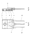
- FIGS.1, 2a-2c and 3a-3b represent an example of a known encapsulation process and the device obtained therewith and of which the description can be found in U.S. patent no. 4,888,307.
- Said device (see FIGS. 1 and 3) comprises a metal plate 2 incorporated in a resin enclosure 3.
- a semiconductor chip 4 is fixed to the metal plate 2, e.g. by welding alloy.
- Metal terminals 5a, 5b are incorporated partly in the resin body 3 and are electrically connected to the plate 4 by wires 6.
- Another central terminal 5 constitutes the plate extension and acts as the transistor collector.
- a passing hole 7 both in the metal plate and in the resin body allows fixing the device on a suitable external support or heat sink. Electrical insulation of the device is provided by the same resin 3 which completely incorporates the metal plate 2, covering its lower surface with a thin insulating layer 8.
- FIGS. 2a-2c illustrate some phases of a known process (in the figures the metal plate of the device, the central terminal and the semiconductor chip are indicated by 31, 38 and 33 respectively). Said phases call for positioning the plate in the cavity of a die 41/42, correct vertical positioning of the plate by means of retractable pins 43, 44 and inlet of resin through the duct 47 (FIG. 2a).
- the pins 43, 44 are retracted and inlet of resin is continued to fill the cavities left by the pins (FIG. 2b).
- the package obtained is extracted from the die by operating the positioning pins 43, 44 and knockout pins 45, 46.
- Insulation obtained with said moulding resin imposes a low defect level in the resin in the package body and in particular in the thin resin layer under the metal plate which must withstand the high insulation tensions. This requirement together with the high hydrodynamic resistance encountered by the resin during input into the die cavity makes it necessary to set high resin injection pressure in the moulding process.
- the encapsulation process requires that, after the first phase of filling the die cavity with epoxy resin and after withdrawal of the pins 43, 44, to fill the cavities left by the pins the input of resin must continue under conditions of higher viscosity. This avoids causing anomalous plate movement but, because of said higher resin viscosity, there is poor compacting of said resin (reduced thickness, porosity, etc.) and resulting poor electrical insulation opposite the retractable position pins.
- Metal plate positioning in the die cavity in accordance with the known art ensures only uniform thickness of the layer 8 of insulation resin (layer involved also in heat dispersion).
- the plate terminal part opposite the one to which leads the central connector is of critical positioning in relation to the die cavity side walls.
- the proper plate position is ensured only in the die part which blocks the central plate connector by adequate locators but this does not ensure centring of the terminal part of the plate (FIG. 3a of the known device showing the plate perfectly centred in relation to the side walls of the resin enclosure is for an ideal case, considering the aforesaid critical plate positioning in the die).
- the plate can be irregularly spaced from the die side walls or even touch them so as to cause loss of electrical insulation in a side wall of the package thus obtained.
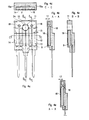
- FIGS.4a-4e illustrate the structure of a device in accordance with the present invention. It is characterized by the structure of the known device principally by the following characteristics:
- These recesses increase the distance 15 between the plate 9 and the walls of the die 13 (said distance goes substantially from 1.0 mm to 2.0 mm) and allows an increase in the flow of resin into the thin insulation layer 16; in this manner the insulation layer 16 is formed of resin coming from two directions: one parallel to that of resin input in the die cavity and the other orthogonal thereto through the lateral recesses 12 present in the plate; the opening 10 and the recesses 12 allow better die filling with low pressures; in addition, once the resin has solidified, these lateral shapes 12 strengthen the zones of lateral hooking 15a of the resin with the plate; said couplings serve to minimize the stresses which the resin induces in the semiconductor chip and in particular during its solidification.
- These channels fill a dual function, i.e. they facilitate running of the resin making less critical the phase of creation of the layer 16 and they improve adhesion between the resin layer 16 and the metal plate 9.
- they facilitate running of the resin making less critical the phase of creation of the layer 16 and they improve adhesion between the resin layer 16 and the metal plate 9.
- these channels increase the contact surface and act as hooking zones between the resin layer 16 and the plate 9 to improve adhesion between these two materials. This eliminates the possibility of detachment of the resin from the metal plate and even subsequent fracturing of the insulation layer 16.
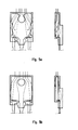
- FIGS.5a-5b show top and side views of the flow lines of the resin in the die cavity during the encapsulation process in accordance with the present 11 invention and the known art. Said figures confirm the utility of the inventive solutions described above in improving filling dynamics because they provide increase in the flow entering the die cavity and facilitated filling of the die cavity on the side under the plate.
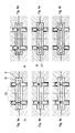
- FIGS.6a-6f illustrate some phases of an encapsulation process in accordance with the present invention designed to ensure correct horizontal positioning of the metal plate inside the die cavity.
- Said figures show the die cavity section along a plane passing through the axes of the two pins nearest the package fixing hole (not shown for the sake of simplicity).
- the positioning pins 20 display on the ends which make contact with the plate 9 during its positioning in the die a tapered point 19 which at its base has a diameter smaller than that of the pins.
- the tapered point forms an angle of approximately 70 and is present only on the die top pins.
- FIG.6a represents the moment when the plate 9 is placed in the cavity 22 of the encapsulation die with its terminal part, which bears the fixing hole (for the sake of simplicity not shown in the figures) in an off centre position.
- FIG. 6b shows the pins in the positioning phase of the plate.
- the tapered point 19 of the pins acts on the hole 18, moving the decentralized plate inside the die cavity and then centring it perfectly.
- FIG. 6c shows the system with the plate correctly positioned at the beginning of filling.
- the diameter of the base of the tapered point less than the diameter of the pins creates an annular surface on which rests the horizontal centring plate and also prevents vertical movement of the plate.
- FIG. 6d shows the die cavity already filled with resin with the plate correctly centred.
- FIG. 6e shows the phase where the pins are withdrawn and the resin continues to flow to fill the cavity 23 left by the pins and the passing holes 18.
- FIG. 6f shows the die cavity entirely filled with resin already solidified and then the semiconductor device with the metal plate perfectly centred inside it and ready to be knocked out in accordance with the known art procedure.
- the passing holes could be blind with depth equal to or greater than the height of the tapered point of the pin.
- the positioning holes could call for the positioning holes, whether passing or blind, to have a form other than round, e.g. elliptical. Indeed, what matters is that the hole have a form, dimensions and allocation such as to allow during positioning of the plate penetration of only the tapered point and not the rest of the pin.
- elliptical holes In case of elliptical holes they must have appropriately their major axis parallel to the axis of the central connector and their minor axis of a length substantially equal to the diameter of the base of the tapered point of the pins.
- the elliptical holes display the advantage, as compared with round holes, of permitting during the transfer moulding process input therein of the resin even when the pins are in fully retracted position (position of FIG. 6d).
- the device with three terminals described can be generalized for other packages completely incorporated in resin and electrically insulated.
- the device in accordance with the present invention can have more than three metal terminals as in integrated circuits.
Landscapes
- Engineering & Computer Science (AREA)
- Manufacturing & Machinery (AREA)
- Mechanical Engineering (AREA)
- Structures Or Materials For Encapsulating Or Coating Semiconductor Devices Or Solid State Devices (AREA)
- Encapsulation Of And Coatings For Semiconductor Or Solid State Devices (AREA)
- Injection Moulding Of Plastics Or The Like (AREA)
- Static Random-Access Memory (AREA)
- Lead Frames For Integrated Circuits (AREA)
- Apparatuses And Processes For Manufacturing Resistors (AREA)
Applications Claiming Priority (2)
| Application Number | Priority Date | Filing Date | Title |
|---|---|---|---|
| ITMI913266A IT1252624B (it) | 1991-12-05 | 1991-12-05 | Dispositivo semiconduttore incapsulato in resina e elettricamente isolato di migliorate caratteristiche di isolamento,e relativo processo di fabbricazione |
| ITMI913266 | 1991-12-05 |
Publications (3)
| Publication Number | Publication Date |
|---|---|
| EP0545487A2 true EP0545487A2 (fr) | 1993-06-09 |
| EP0545487A3 EP0545487A3 (en) | 1994-06-08 |
| EP0545487B1 EP0545487B1 (fr) | 1997-08-06 |
Family
ID=11361268
Family Applications (1)
| Application Number | Title | Priority Date | Filing Date |
|---|---|---|---|
| EP92203676A Expired - Lifetime EP0545487B1 (fr) | 1991-12-05 | 1992-11-27 | Dispositif semi-conducteur encapsulé en résine |
Country Status (5)
| Country | Link |
|---|---|
| US (2) | US5514913A (fr) |
| EP (1) | EP0545487B1 (fr) |
| JP (1) | JP3338490B2 (fr) |
| DE (1) | DE69221440T2 (fr) |
| IT (1) | IT1252624B (fr) |
Cited By (7)
| Publication number | Priority date | Publication date | Assignee | Title |
|---|---|---|---|---|
| DE4340862A1 (de) * | 1993-12-01 | 1995-06-08 | Telefunken Microelectron | Vergießvorrichtung zum Herstellen von optoelektronischen Bauelementen |
| EP0782184A1 (fr) * | 1995-12-29 | 1997-07-02 | STMicroelectronics S.r.l. | Structure de dissipateur de chaleur et de support pour un boîtier |
| EP0817261A1 (fr) * | 1996-06-28 | 1998-01-07 | STMicroelectronics S.r.l. | Procédé de fabrication d'un boítier en plastique pour circuit électronique ayant un dissipateur de chaleur complètement isolé |
| US5793613A (en) * | 1995-12-29 | 1998-08-11 | Sgs-Thomson Microelectronics S.R.1. | Heat-dissipating and supporting structure for a plastic package with a fully insulated heat sink for an electronic device |
| FR2844219A1 (fr) * | 2002-09-09 | 2004-03-12 | Valeo Electronique Sys Liaison | Moule de surmoulage |
| WO2011057662A1 (fr) * | 2009-11-11 | 2011-05-19 | Datalogic Automation S.R.L. | Procédé pour moulage par injection d'un boîtier externe d'un objet, objet et appareil pour moulage par injection |
| JP2019511964A (ja) * | 2016-01-19 | 2019-05-09 | ヴァレオ、コンフォート、アンド、ドライビング、アシスタンスValeo Comfort And Driving Assistance | 漏れ止め電子デバイス及びそれを得る方法 |
Families Citing this family (26)
| Publication number | Priority date | Publication date | Assignee | Title |
|---|---|---|---|---|
| JPH08204099A (ja) * | 1995-01-31 | 1996-08-09 | Rohm Co Ltd | 半導体装置の構造及び形成方法 |
| JP3389775B2 (ja) * | 1995-05-19 | 2003-03-24 | 株式会社デンソー | インサート品成形方法およびインサート品成形装置 |
| JP2781783B2 (ja) * | 1996-07-30 | 1998-07-30 | 山形日本電気株式会社 | 半導体装置用パッケージ |
| DE10023208A1 (de) * | 2000-05-12 | 2001-11-15 | Alstom Power Nv | Isolierung von Statorwicklungen im Spritzgussverfahren |
| US6365434B1 (en) | 2000-06-28 | 2002-04-02 | Micron Technology, Inc. | Method and apparatus for reduced flash encapsulation of microelectronic devices |
| NZ531008A (en) * | 2001-08-10 | 2006-08-31 | Black & Decker Inc | Electrically isolated module |
| US7109064B2 (en) * | 2003-12-08 | 2006-09-19 | Semiconductor Components Industries, L.L.C. | Method of forming a semiconductor package and leadframe therefor |
| WO2007010315A2 (fr) * | 2005-07-20 | 2007-01-25 | Infineon Technologies Ag | Plaquette de grille de connexions et appareil de moulage pour un composant electronique et procede d'encapsulation d'un composant electronique |
| US7923827B2 (en) * | 2005-07-28 | 2011-04-12 | Infineon Technologies Ag | Semiconductor module for a switched-mode power supply and method for its assembly |
| WO2007074352A1 (fr) * | 2005-12-29 | 2007-07-05 | Infineon Technologies Ag | Composant électronique et procédé de fabrication d’un composant électronique |
| AU2007284651B2 (en) | 2006-08-09 | 2014-03-20 | Institute For Systems Biology | Organ-specific proteins and methods of their use |
| US7875962B2 (en) * | 2007-10-15 | 2011-01-25 | Power Integrations, Inc. | Package for a power semiconductor device |
| US8067841B2 (en) * | 2008-02-25 | 2011-11-29 | Infineon Technologies Ag | Semiconductor devices having a resin with warpage compensated surfaces |
| US7839004B2 (en) * | 2008-07-30 | 2010-11-23 | Sanyo Electric Co., Ltd. | Semiconductor device, semiconductor module, method for manufacturing semiconductor device, and lead frame |
| JP2010103279A (ja) * | 2008-10-23 | 2010-05-06 | Shindengen Electric Mfg Co Ltd | 半導体装置 |
| DE102008061617A1 (de) * | 2008-12-11 | 2010-06-17 | Trw Automotive Gmbh | Verfahren und Werkzeug zur Herstellung eines elektronischen Bauteils mit einem kunststoffumspritzten Träger |
| CN102230991B (zh) * | 2009-10-23 | 2013-01-09 | 鸿富锦精密工业(深圳)有限公司 | 光纤耦合连接器 |
| JP5549491B2 (ja) * | 2010-09-06 | 2014-07-16 | 日立金属株式会社 | バスバーモジュールの製造方法、及びバスバーモジュール |
| US20160277017A1 (en) * | 2011-09-13 | 2016-09-22 | Fsp Technology Inc. | Snubber circuit |
| JP6162643B2 (ja) | 2014-05-21 | 2017-07-12 | 三菱電機株式会社 | 半導体装置 |
| US10232531B1 (en) * | 2014-07-08 | 2019-03-19 | Verily Life Sciences Llc | Methods and apparatus for forming a polymer layer around a structure using a plurality of protrusions |
| JP6745645B2 (ja) * | 2016-05-25 | 2020-08-26 | オリンパス株式会社 | インサート成形方法 |
| CN106601714A (zh) * | 2017-01-25 | 2017-04-26 | 长电科技(宿迁)有限公司 | 一种活动顶针内绝缘封装结构及其工艺方法 |
| JP6448712B2 (ja) * | 2017-06-15 | 2019-01-09 | 三菱電機株式会社 | 半導体装置 |
| JP6888525B2 (ja) * | 2017-11-06 | 2021-06-16 | 株式会社デンソー | 通電部材モジュールの製造方法 |
| EP3916910B1 (fr) | 2020-05-26 | 2022-12-14 | Premo, S.A. | Antenne basse fréquence longue portée |
Citations (1)
| Publication number | Priority date | Publication date | Assignee | Title |
|---|---|---|---|---|
| US4888307A (en) | 1986-08-27 | 1989-12-19 | Sgs Microelettronica S.P.A. | Method for manufacturing plastic encapsulated semiconductor devices |
Family Cites Families (28)
| Publication number | Priority date | Publication date | Assignee | Title |
|---|---|---|---|---|
| US3715423A (en) * | 1971-01-25 | 1973-02-06 | Motorola Inc | Plastic encapsulation of semiconductor devices |
| JPS5238885A (en) * | 1975-09-22 | 1977-03-25 | Nec Home Electronics Ltd | Method for production of semiconductor device |
| JPS5565450A (en) * | 1978-11-10 | 1980-05-16 | Hitachi Ltd | Resin-mold type semiconductor device |
| US4266267A (en) * | 1979-11-19 | 1981-05-05 | General Electric Company | Mounting arrangement for transistors and the like |
| WO1982003294A1 (fr) * | 1981-03-23 | 1982-09-30 | Inc Motorola | Dispositif a semi-conducteur comprenant un boitier sans placage |
| JPS5917273A (ja) * | 1982-07-20 | 1984-01-28 | Nec Corp | 樹脂封止半導体装置 |
| GB8308751D0 (en) * | 1983-03-30 | 1983-05-11 | Era Patents Ltd | Mounting of semiconductor devices |
| JPS6156420A (ja) * | 1984-07-31 | 1986-03-22 | Sanken Electric Co Ltd | 樹脂封止形半導体装置の製造方法 |
| JPS6180845A (ja) * | 1984-09-28 | 1986-04-24 | Hitachi Ltd | 半導体装置 |
| JPS61102040A (ja) * | 1984-10-25 | 1986-05-20 | Sanken Electric Co Ltd | 樹脂封止型半導体装置の製造方法 |
| JPS61219144A (ja) * | 1985-03-25 | 1986-09-29 | Sanken Electric Co Ltd | 樹脂封止型半導体装置の製造方法 |
| JPS60242649A (ja) * | 1985-03-29 | 1985-12-02 | Hitachi Ltd | 樹脂封止型半導体装置 |
| JPS6193652A (ja) * | 1985-09-06 | 1986-05-12 | Hitachi Ltd | 樹脂封止型半導体装置 |
| JPS62154656A (ja) * | 1985-12-27 | 1987-07-09 | Toshiba Corp | 樹脂封止型半導体装置の製造方法 |
| JP2507343B2 (ja) * | 1986-09-08 | 1996-06-12 | 株式会社東芝 | 樹脂封止型半導体装置 |
| JPS6378558A (ja) * | 1986-09-22 | 1988-04-08 | Hitachi Ltd | 電子装置 |
| FR2607338A1 (fr) * | 1986-11-21 | 1988-05-27 | Eurotechnique Sa | Circuit de commutation de tension en technologie mos |
| JPS63170949A (ja) * | 1987-01-09 | 1988-07-14 | Fuji Electric Co Ltd | 半導体装置 |
| JPS63208255A (ja) * | 1987-02-25 | 1988-08-29 | Hitachi Ltd | 電子装置 |
| JPS63213362A (ja) * | 1987-02-27 | 1988-09-06 | Mitsubishi Electric Corp | 樹脂封止型半導体装置 |
| JPS6442844A (en) * | 1987-08-10 | 1989-02-15 | Fuji Electric Co Ltd | Lead frame for semiconductor device |
| JPH01258452A (ja) * | 1988-04-08 | 1989-10-16 | Nec Corp | 樹脂封止半導体装置 |
| JPH01315147A (ja) * | 1989-04-07 | 1989-12-20 | Sanken Electric Co Ltd | 樹脂封止形半導体装置の製造方法 |
| JPH02268457A (ja) * | 1989-04-10 | 1990-11-02 | Nec Corp | 樹脂封止型半導体装置 |
| JPH0353551A (ja) * | 1989-07-21 | 1991-03-07 | Nec Corp | 絶縁型半導体装置用放熱板 |
| JP2755440B2 (ja) * | 1989-07-28 | 1998-05-20 | 関西日本電気株式会社 | 樹脂モールド型半導体装置及び樹脂モールド装置 |
| JPH03108744A (ja) * | 1989-09-22 | 1991-05-08 | Toshiba Corp | 樹脂封止型半導体装置 |
| US5105259A (en) * | 1990-09-28 | 1992-04-14 | Motorola, Inc. | Thermally enhanced semiconductor device utilizing a vacuum to ultimately enhance thermal dissipation |
-
1991
- 1991-12-05 IT ITMI913266A patent/IT1252624B/it active IP Right Grant
-
1992
- 1992-11-25 JP JP31519692A patent/JP3338490B2/ja not_active Expired - Fee Related
- 1992-11-27 DE DE69221440T patent/DE69221440T2/de not_active Expired - Fee Related
- 1992-11-27 EP EP92203676A patent/EP0545487B1/fr not_active Expired - Lifetime
- 1992-12-07 US US07/987,490 patent/US5514913A/en not_active Expired - Lifetime
-
1995
- 1995-02-06 US US08/384,753 patent/US5766985A/en not_active Expired - Lifetime
Patent Citations (1)
| Publication number | Priority date | Publication date | Assignee | Title |
|---|---|---|---|---|
| US4888307A (en) | 1986-08-27 | 1989-12-19 | Sgs Microelettronica S.P.A. | Method for manufacturing plastic encapsulated semiconductor devices |
Cited By (10)
| Publication number | Priority date | Publication date | Assignee | Title |
|---|---|---|---|---|
| DE4340862A1 (de) * | 1993-12-01 | 1995-06-08 | Telefunken Microelectron | Vergießvorrichtung zum Herstellen von optoelektronischen Bauelementen |
| DE4340862C2 (de) * | 1993-12-01 | 2002-04-11 | Vishay Semiconductor Gmbh | Vergießvorrichtung zum Herstellen von optoelektronischen Bauelementen |
| EP0782184A1 (fr) * | 1995-12-29 | 1997-07-02 | STMicroelectronics S.r.l. | Structure de dissipateur de chaleur et de support pour un boîtier |
| US5793613A (en) * | 1995-12-29 | 1998-08-11 | Sgs-Thomson Microelectronics S.R.1. | Heat-dissipating and supporting structure for a plastic package with a fully insulated heat sink for an electronic device |
| EP0817261A1 (fr) * | 1996-06-28 | 1998-01-07 | STMicroelectronics S.r.l. | Procédé de fabrication d'un boítier en plastique pour circuit électronique ayant un dissipateur de chaleur complètement isolé |
| US5935502A (en) * | 1996-06-28 | 1999-08-10 | Sgs-Thomson Microelectronics | Method for manufacturing plastic package for electronic device having a fully insulated dissipator |
| FR2844219A1 (fr) * | 2002-09-09 | 2004-03-12 | Valeo Electronique Sys Liaison | Moule de surmoulage |
| WO2011057662A1 (fr) * | 2009-11-11 | 2011-05-19 | Datalogic Automation S.R.L. | Procédé pour moulage par injection d'un boîtier externe d'un objet, objet et appareil pour moulage par injection |
| US8936200B2 (en) | 2009-11-11 | 2015-01-20 | Balluff Gmbh | Method for injection moulding an external housing of an object, object and apparatus for injection moulding |
| JP2019511964A (ja) * | 2016-01-19 | 2019-05-09 | ヴァレオ、コンフォート、アンド、ドライビング、アシスタンスValeo Comfort And Driving Assistance | 漏れ止め電子デバイス及びそれを得る方法 |
Also Published As
| Publication number | Publication date |
|---|---|
| DE69221440D1 (de) | 1997-09-11 |
| EP0545487B1 (fr) | 1997-08-06 |
| US5766985A (en) | 1998-06-16 |
| JP3338490B2 (ja) | 2002-10-28 |
| DE69221440T2 (de) | 1998-01-29 |
| ITMI913266A1 (it) | 1993-06-05 |
| US5514913A (en) | 1996-05-07 |
| ITMI913266A0 (it) | 1991-12-05 |
| IT1252624B (it) | 1995-06-19 |
| EP0545487A3 (en) | 1994-06-08 |
| JPH05235074A (ja) | 1993-09-10 |
Similar Documents
| Publication | Publication Date | Title |
|---|---|---|
| EP0545487A2 (fr) | Dispositif semi-conducteur encapsulé en résine et isolé électriquement ayant des caractéristiques d'isolation améliorées et procédé de fabrication associé | |
| US3431092A (en) | Lead frame members for semiconductor devices | |
| US5935502A (en) | Method for manufacturing plastic package for electronic device having a fully insulated dissipator | |
| EP1005085B1 (fr) | Dispositif électronique encapsulé en résine | |
| US4589010A (en) | Method for manufacturing a plastic encapsulated semiconductor device and a lead frame therefor | |
| EP0577966A1 (fr) | Empaquetage en plastique à contrainte réduite | |
| KR0144164B1 (ko) | 엘오씨 반도체 패키지 및 반도체 장치를 패키징하는 방법 | |
| US5384286A (en) | Process for encapsulating a semiconductor chip, leadframe and heatsink | |
| CN101350319B (zh) | 用来制作封装半导体器件的方法和系统 | |
| US5953593A (en) | Method and mold for manufacturing a plastic package for an electronic device having a heat sink | |
| US5757067A (en) | Resin-sealed type semiconductor device | |
| US8056225B2 (en) | Method for manufacturing electrical connectors for enhancing coplanarity | |
| TW444309B (en) | Improved leadframe structure with locked inner leads and process for manufacturing same | |
| JPH0739241Y2 (ja) | 樹脂封止型半導体装置用リードフレーム | |
| JPH1064933A (ja) | 樹脂封止型半導体装置及びその製造方法 | |
| KR0138295Y1 (ko) | 하이핀 패키지용 수지기판 몰딩장치 | |
| JPS6194349A (ja) | 樹脂封止形半導体装置の製造方法及びその製造方法に使用するリ−ドフレ−ム | |
| JPH0563937B2 (fr) | ||
| KR200289924Y1 (ko) | 리드프레임 | |
| JP2858690B2 (ja) | 樹脂封止型電子部品の製造方法 | |
| JPS62183130A (ja) | 樹脂封止による半導体装置の製造方法 | |
| JPS61135129A (ja) | 樹脂封止型半導体装置の製造方法 | |
| JPH0242751A (ja) | 樹脂封止形半導体装置の製造方法 | |
| CN112935452A (zh) | 一种珠状热敏电阻器与导线焊接装置及焊接方法 | |
| JPH02159750A (ja) | 半導体装置の製造方法 |
Legal Events
| Date | Code | Title | Description |
|---|---|---|---|
| PUAI | Public reference made under article 153(3) epc to a published international application that has entered the european phase |
Free format text: ORIGINAL CODE: 0009012 |
|
| AK | Designated contracting states |
Kind code of ref document: A2 Designated state(s): DE FR GB |
|
| PUAL | Search report despatched |
Free format text: ORIGINAL CODE: 0009013 |
|
| AK | Designated contracting states |
Kind code of ref document: A3 Designated state(s): DE FR GB |
|
| 17P | Request for examination filed |
Effective date: 19940908 |
|
| 17Q | First examination report despatched |
Effective date: 19950705 |
|
| GRAG | Despatch of communication of intention to grant |
Free format text: ORIGINAL CODE: EPIDOS AGRA |
|
| GRAH | Despatch of communication of intention to grant a patent |
Free format text: ORIGINAL CODE: EPIDOS IGRA |
|
| GRAH | Despatch of communication of intention to grant a patent |
Free format text: ORIGINAL CODE: EPIDOS IGRA |
|
| GRAA | (expected) grant |
Free format text: ORIGINAL CODE: 0009210 |
|
| AK | Designated contracting states |
Kind code of ref document: B1 Designated state(s): DE FR GB |
|
| REF | Corresponds to: |
Ref document number: 69221440 Country of ref document: DE Date of ref document: 19970911 |
|
| ET | Fr: translation filed | ||
| PLBE | No opposition filed within time limit |
Free format text: ORIGINAL CODE: 0009261 |
|
| 26N | No opposition filed | ||
| REG | Reference to a national code |
Ref country code: GB Ref legal event code: IF02 |
|
| PGFP | Annual fee paid to national office [announced via postgrant information from national office to epo] |
Ref country code: DE Payment date: 20021128 Year of fee payment: 11 |
|
| PG25 | Lapsed in a contracting state [announced via postgrant information from national office to epo] |
Ref country code: DE Free format text: LAPSE BECAUSE OF NON-PAYMENT OF DUE FEES Effective date: 20040602 |
|
| PGFP | Annual fee paid to national office [announced via postgrant information from national office to epo] |
Ref country code: FR Payment date: 20041109 Year of fee payment: 13 |
|
| PGFP | Annual fee paid to national office [announced via postgrant information from national office to epo] |
Ref country code: GB Payment date: 20041124 Year of fee payment: 13 |
|
| PG25 | Lapsed in a contracting state [announced via postgrant information from national office to epo] |
Ref country code: GB Free format text: LAPSE BECAUSE OF NON-PAYMENT OF DUE FEES Effective date: 20051127 |
|
| GBPC | Gb: european patent ceased through non-payment of renewal fee |
Effective date: 20051127 |
|
| PG25 | Lapsed in a contracting state [announced via postgrant information from national office to epo] |
Ref country code: FR Free format text: LAPSE BECAUSE OF NON-PAYMENT OF DUE FEES Effective date: 20060731 |
|
| REG | Reference to a national code |
Ref country code: FR Ref legal event code: ST Effective date: 20060731 |