EP0553855A2 - Dispositif semi-conducteur et procédé de sa fabrication - Google Patents
Dispositif semi-conducteur et procédé de sa fabrication Download PDFInfo
- Publication number
- EP0553855A2 EP0553855A2 EP93101416A EP93101416A EP0553855A2 EP 0553855 A2 EP0553855 A2 EP 0553855A2 EP 93101416 A EP93101416 A EP 93101416A EP 93101416 A EP93101416 A EP 93101416A EP 0553855 A2 EP0553855 A2 EP 0553855A2
- Authority
- EP
- European Patent Office
- Prior art keywords
- porous
- amorphous
- layer
- substrate
- etching
- Prior art date
- Legal status (The legal status is an assumption and is not a legal conclusion. Google has not performed a legal analysis and makes no representation as to the accuracy of the status listed.)
- Granted
Links
Images


Classifications
-
- H—ELECTRICITY
- H10—SEMICONDUCTOR DEVICES; ELECTRIC SOLID-STATE DEVICES NOT OTHERWISE PROVIDED FOR
- H10P—GENERIC PROCESSES OR APPARATUS FOR THE MANUFACTURE OR TREATMENT OF DEVICES COVERED BY CLASS H10
- H10P14/00—Formation of materials, e.g. in the shape of layers or pillars
- H10P14/20—Formation of materials, e.g. in the shape of layers or pillars of semiconductor materials
- H10P14/24—Formation of materials, e.g. in the shape of layers or pillars of semiconductor materials using chemical vapour deposition [CVD]
-
- H—ELECTRICITY
- H10—SEMICONDUCTOR DEVICES; ELECTRIC SOLID-STATE DEVICES NOT OTHERWISE PROVIDED FOR
- H10P—GENERIC PROCESSES OR APPARATUS FOR THE MANUFACTURE OR TREATMENT OF DEVICES COVERED BY CLASS H10
- H10P14/00—Formation of materials, e.g. in the shape of layers or pillars
- H10P14/20—Formation of materials, e.g. in the shape of layers or pillars of semiconductor materials
- H10P14/22—Formation of materials, e.g. in the shape of layers or pillars of semiconductor materials using physical deposition, e.g. vacuum deposition or sputtering
-
- H—ELECTRICITY
- H10—SEMICONDUCTOR DEVICES; ELECTRIC SOLID-STATE DEVICES NOT OTHERWISE PROVIDED FOR
- H10P—GENERIC PROCESSES OR APPARATUS FOR THE MANUFACTURE OR TREATMENT OF DEVICES COVERED BY CLASS H10
- H10P14/00—Formation of materials, e.g. in the shape of layers or pillars
- H10P14/20—Formation of materials, e.g. in the shape of layers or pillars of semiconductor materials
- H10P14/27—Formation of materials, e.g. in the shape of layers or pillars of semiconductor materials using selective deposition, e.g. simultaneous growth of monocrystalline and non-monocrystalline semiconductor materials
- H10P14/271—Formation of materials, e.g. in the shape of layers or pillars of semiconductor materials using selective deposition, e.g. simultaneous growth of monocrystalline and non-monocrystalline semiconductor materials characterised by the preparation of substrate for selective deposition
-
- H—ELECTRICITY
- H10—SEMICONDUCTOR DEVICES; ELECTRIC SOLID-STATE DEVICES NOT OTHERWISE PROVIDED FOR
- H10P—GENERIC PROCESSES OR APPARATUS FOR THE MANUFACTURE OR TREATMENT OF DEVICES COVERED BY CLASS H10
- H10P14/00—Formation of materials, e.g. in the shape of layers or pillars
- H10P14/20—Formation of materials, e.g. in the shape of layers or pillars of semiconductor materials
- H10P14/29—Formation of materials, e.g. in the shape of layers or pillars of semiconductor materials characterised by the substrates
- H10P14/2901—Materials
- H10P14/2902—Materials being Group IVA materials
- H10P14/2905—Silicon, silicon germanium or germanium
-
- H—ELECTRICITY
- H10—SEMICONDUCTOR DEVICES; ELECTRIC SOLID-STATE DEVICES NOT OTHERWISE PROVIDED FOR
- H10P—GENERIC PROCESSES OR APPARATUS FOR THE MANUFACTURE OR TREATMENT OF DEVICES COVERED BY CLASS H10
- H10P14/00—Formation of materials, e.g. in the shape of layers or pillars
- H10P14/20—Formation of materials, e.g. in the shape of layers or pillars of semiconductor materials
- H10P14/29—Formation of materials, e.g. in the shape of layers or pillars of semiconductor materials characterised by the substrates
- H10P14/2901—Materials
- H10P14/2921—Materials being crystalline insulating materials
-
- H—ELECTRICITY
- H10—SEMICONDUCTOR DEVICES; ELECTRIC SOLID-STATE DEVICES NOT OTHERWISE PROVIDED FOR
- H10P—GENERIC PROCESSES OR APPARATUS FOR THE MANUFACTURE OR TREATMENT OF DEVICES COVERED BY CLASS H10
- H10P14/00—Formation of materials, e.g. in the shape of layers or pillars
- H10P14/20—Formation of materials, e.g. in the shape of layers or pillars of semiconductor materials
- H10P14/29—Formation of materials, e.g. in the shape of layers or pillars of semiconductor materials characterised by the substrates
- H10P14/2901—Materials
- H10P14/2922—Materials being non-crystalline insulating materials, e.g. glass or polymers
-
- H—ELECTRICITY
- H10—SEMICONDUCTOR DEVICES; ELECTRIC SOLID-STATE DEVICES NOT OTHERWISE PROVIDED FOR
- H10P—GENERIC PROCESSES OR APPARATUS FOR THE MANUFACTURE OR TREATMENT OF DEVICES COVERED BY CLASS H10
- H10P14/00—Formation of materials, e.g. in the shape of layers or pillars
- H10P14/20—Formation of materials, e.g. in the shape of layers or pillars of semiconductor materials
- H10P14/32—Formation of materials, e.g. in the shape of layers or pillars of semiconductor materials characterised by intermediate layers between substrates and deposited layers
- H10P14/3202—Materials thereof
- H10P14/3238—Materials thereof being insulating materials
-
- H—ELECTRICITY
- H10—SEMICONDUCTOR DEVICES; ELECTRIC SOLID-STATE DEVICES NOT OTHERWISE PROVIDED FOR
- H10P—GENERIC PROCESSES OR APPARATUS FOR THE MANUFACTURE OR TREATMENT OF DEVICES COVERED BY CLASS H10
- H10P14/00—Formation of materials, e.g. in the shape of layers or pillars
- H10P14/20—Formation of materials, e.g. in the shape of layers or pillars of semiconductor materials
- H10P14/34—Deposited materials, e.g. layers
- H10P14/3402—Deposited materials, e.g. layers characterised by the chemical composition
- H10P14/3404—Deposited materials, e.g. layers characterised by the chemical composition being Group IVA materials
- H10P14/3411—Silicon, silicon germanium or germanium
-
- H—ELECTRICITY
- H10—SEMICONDUCTOR DEVICES; ELECTRIC SOLID-STATE DEVICES NOT OTHERWISE PROVIDED FOR
- H10P—GENERIC PROCESSES OR APPARATUS FOR THE MANUFACTURE OR TREATMENT OF DEVICES COVERED BY CLASS H10
- H10P14/00—Formation of materials, e.g. in the shape of layers or pillars
- H10P14/20—Formation of materials, e.g. in the shape of layers or pillars of semiconductor materials
- H10P14/34—Deposited materials, e.g. layers
- H10P14/3402—Deposited materials, e.g. layers characterised by the chemical composition
- H10P14/3414—Deposited materials, e.g. layers characterised by the chemical composition being group IIIA-VIA materials
- H10P14/3421—Arsenides
-
- H—ELECTRICITY
- H10—SEMICONDUCTOR DEVICES; ELECTRIC SOLID-STATE DEVICES NOT OTHERWISE PROVIDED FOR
- H10P—GENERIC PROCESSES OR APPARATUS FOR THE MANUFACTURE OR TREATMENT OF DEVICES COVERED BY CLASS H10
- H10P14/00—Formation of materials, e.g. in the shape of layers or pillars
- H10P14/20—Formation of materials, e.g. in the shape of layers or pillars of semiconductor materials
- H10P14/34—Deposited materials, e.g. layers
- H10P14/3451—Structure
- H10P14/3452—Microstructure
- H10P14/3458—Monocrystalline
-
- H—ELECTRICITY
- H10—SEMICONDUCTOR DEVICES; ELECTRIC SOLID-STATE DEVICES NOT OTHERWISE PROVIDED FOR
- H10P—GENERIC PROCESSES OR APPARATUS FOR THE MANUFACTURE OR TREATMENT OF DEVICES COVERED BY CLASS H10
- H10P14/00—Formation of materials, e.g. in the shape of layers or pillars
- H10P14/20—Formation of materials, e.g. in the shape of layers or pillars of semiconductor materials
- H10P14/38—Formation of materials, e.g. in the shape of layers or pillars of semiconductor materials characterised by treatments done after the formation of the materials
- H10P14/3802—Crystallisation or recrystallisation of non-monocrystalline semiconductor materials, e.g. regrowth
-
- H—ELECTRICITY
- H10—SEMICONDUCTOR DEVICES; ELECTRIC SOLID-STATE DEVICES NOT OTHERWISE PROVIDED FOR
- H10P—GENERIC PROCESSES OR APPARATUS FOR THE MANUFACTURE OR TREATMENT OF DEVICES COVERED BY CLASS H10
- H10P50/00—Etching of wafers, substrates or parts of devices
- H10P50/60—Wet etching
- H10P50/64—Wet etching of semiconductor materials
- H10P50/642—Chemical etching
-
- H—ELECTRICITY
- H10—SEMICONDUCTOR DEVICES; ELECTRIC SOLID-STATE DEVICES NOT OTHERWISE PROVIDED FOR
- H10P—GENERIC PROCESSES OR APPARATUS FOR THE MANUFACTURE OR TREATMENT OF DEVICES COVERED BY CLASS H10
- H10P90/00—Preparation of wafers not covered by a single main group of this subclass, e.g. wafer reinforcement
- H10P90/19—Preparing inhomogeneous wafers
- H10P90/1904—Preparing vertically inhomogeneous wafers
- H10P90/1906—Preparing SOI wafers
- H10P90/1914—Preparing SOI wafers using bonding
-
- H—ELECTRICITY
- H10—SEMICONDUCTOR DEVICES; ELECTRIC SOLID-STATE DEVICES NOT OTHERWISE PROVIDED FOR
- H10P—GENERIC PROCESSES OR APPARATUS FOR THE MANUFACTURE OR TREATMENT OF DEVICES COVERED BY CLASS H10
- H10P90/00—Preparation of wafers not covered by a single main group of this subclass, e.g. wafer reinforcement
- H10P90/19—Preparing inhomogeneous wafers
- H10P90/1904—Preparing vertically inhomogeneous wafers
- H10P90/1906—Preparing SOI wafers
- H10P90/1922—Preparing SOI wafers using silicon etch back techniques, e.g. BESOI or ELTRAN
-
- H—ELECTRICITY
- H10—SEMICONDUCTOR DEVICES; ELECTRIC SOLID-STATE DEVICES NOT OTHERWISE PROVIDED FOR
- H10W—GENERIC PACKAGES, INTERCONNECTIONS, CONNECTORS OR OTHER CONSTRUCTIONAL DETAILS OF DEVICES COVERED BY CLASS H10
- H10W10/00—Isolation regions in semiconductor bodies between components of integrated devices
- H10W10/10—Isolation regions comprising dielectric materials
- H10W10/181—Semiconductor-on-insulator [SOI] isolation regions, e.g. buried oxide regions of SOI wafers
-
- Y—GENERAL TAGGING OF NEW TECHNOLOGICAL DEVELOPMENTS; GENERAL TAGGING OF CROSS-SECTIONAL TECHNOLOGIES SPANNING OVER SEVERAL SECTIONS OF THE IPC; TECHNICAL SUBJECTS COVERED BY FORMER USPC CROSS-REFERENCE ART COLLECTIONS [XRACs] AND DIGESTS
- Y10—TECHNICAL SUBJECTS COVERED BY FORMER USPC
- Y10S—TECHNICAL SUBJECTS COVERED BY FORMER USPC CROSS-REFERENCE ART COLLECTIONS [XRACs] AND DIGESTS
- Y10S438/00—Semiconductor device manufacturing: process
- Y10S438/977—Thinning or removal of substrate
Definitions
- the present invention relates to a semiconductor device substrate (a substrate for a semiconductor device) which is composed of monocrystal formed on an insulator and is useful widely for large-scale integrated circuits and the like.
- the present invention also relates to a process for producing the above semiconductor device substrate.
- SOI silicon-on-insulator technique
- an SOS technique silicon-on-sapphire which forms heteroepitaxial Si on monocrystalline sapphire substrate by CVD (chemical vapor deposition).
- CVD chemical vapor deposition
- a first method comprises steps of oxidizing a surface of an monocrystalline Si substrate, forming an aperture in the oxidized layer to uncover partially the Si substrate, growing Si epitaxially in a lateral direction using the uncovered Si as the seed to form an monocrystalline Si layer on the SiO2 (Si layer being deposited on SiO2); and a second method comprises steps of forming SiO2 under the monocrystalline Si substrate by use of the monocrystalline Si substrate itself as the active layer (no Si layer being deposited).
- the solid-phase epitaxial growth is classified into vertical solid-phase epitaxial growth and lateral solid-phase epitaxial growth.
- the vertical solid-phase epitaxial growth is employed chiefly for crystallinity recovery after ion implantation.
- the lateral solid-phase epitaxial growth is suitable.
- SiO2 having an aperture is formed on an Si substrate; amorphous Si is deposited over the entire face of the substrate; the vertical solid-phase epitaxial growth is carried out through the aperture; and then the lateral solid-phase epitaxial growth is carried out over the formed SiO2.
- the solid-phase epitaxial growth is practicable at temperature of as low as about 600°C.
- the SOI structure formation through the above-described solid-phase epitaxial growth involves problems below:
- all the monocrystalline Si region has to be formed in the face direction, which necessitates growth in long distance and long time.
- the long growth time causes formation of nuclei in the amorphous Si, which inhibits the growth, and results in insufficient growth distance of only several ⁇ m.
- countermeasures are taken such as adjustment of the pressure and beam irradiation to extend the growth distance, and introduction of an impurity to increase the growth velocity.
- the growth distance in lateral direction is limited to several tens of ⁇ m at the largest, and an SOI of a larger area cannot be formed.
- the lateral solid-phase epitaxial growth is known to result in remarkably low crystallinity than the vertical solid-phase epitaxial growth and to cause a number of dislocation and twinning, which impairs directly the device properties.
- Known techniques for forming the SOI structure by deposition include direct lateral epitaxial growth of monocrystalline Si by CVD; deposition of amorphous Si and subsequent lateral solid-phase epitaxial growth by heat treatment; irradiation of a focused energy beam such as electron beam and laser light beam on polycrystalline Si layer to grow monocrystalline layer on SiO2 by melt-recrystallization; and scanning with a bar-shaped heater over a molten zone (zone melting recrystallization).
- the CVD process requires sacrificial oxidation for forming a thin flat film.
- the lateral solid-phase growth results in low crystallinity.
- the beam annealing process involves problems in treating time by a converged beam, control of superposition of the beam and focus adjustment.
- zone melting recrystallization is most highly developed, and has been employed for experimental production of relatively large integrated circuits. This method, however, still causes crystal defects in subgrain boundary, etc., and does not give a minority carrier device.
- This method is a laser recrystallization method having some problems in treating time of scanning a converged beam and control of superposition of the beam and focus adjustment and poor productivity, and therefore it is not industrially applied. Furthermore, since the seed for the laser recrystallization is formed by a solid-phase epitaxial growth from the external seed, the steps thereof are complicated and finally the crystallinity of the epitaxial Si layer remarkably goes bad in comparison with that of the original monocrystalline external seed. In addition, there is a problem that the external seed can not easily removed since it is bonded to the epitaxial layer by valence bond.
- Ni silicide the lattice coherency with si is very good, but the crystallization temperature of Ni silicide is 750 °C or higher. Therefore, there is a problem that generation of nuclei in amorphous Si occurs to form polycrystal before epitaxial growth of Ni silicide. Furthermore, there is a problem that the lattice coherency of Co silicide having low crystallization temperature with Si is not good.
- this method can not satisfy formation of a good epitaxial Si layer and removal of seed at the same time.
- a substrate made of a different material such as light-transmissive substrate typified by glass allows a deposited thin Si layer to grow only into an amorphous or polycrystalline layer under the influence of the disorderness of the crystal structure of the substrate, and therefore is unsuitable for production of devices of high performance. It is due to the amorphousness or the difference in periodicity of crystal structure of the substrate. Therefore, simple deposition of Si layer will not give excellent monocrystal layer.
- the light-transmissive substrate is important in constructing a light-receiving device for a contact sensor, a projection type liquid crystal image displaying apparatus, and the like.
- a sensor or image element (picture element) of a display apparatus in higher density, higher resolution, and higher fineness, high performance of the driving device is required. Therefore, the device on a light-transmissive substrate have to be made from monocrystal layer having excellent crystallinity.
- amorphous Si or polycrystalline Si will not generally give a driving device which exhibits the satisfactory performance required nowadays or to be required in the future because of many defects in the crystal structure.
- monocrystalline Si on another kind of material is an important technique in forming a three-dimensional combination with another functional device or in use, as a substrate, of material having properties not obtained by Si such as light transmissivity, high heat releasability, high mechanical strength, and low cost.
- the formation of excellent monocrystalline Si film on such a material is extremely difficult.
- This thin film formation is practicable in two ways: (1) thin film formation by polishing, and (2) thin film formation by selective etching.
- the former method i.e., polishing
- the variation of the film thickness amounts to several tens of %, which is a serious problem.
- the thin film formation is much more difficult.
- the latter method i.e., the selective etching, although it is considered to be effective in formation of a uniform thin film, involves problems such that the selectivity is 102 or lower and is insufficient; the surface property is inferior after etching; the crystallinity of the SOI layer is low as the result of utilizing ion implantation and epitaxial growth or heteroepitaxial growth on an Si layer doped with B in high density (C. Harendt, et al., J. Elect. Mater., Vol.20, p.267 (1991); H. Baumgart, et al., Extended Abstract of ECS 1st International Symposium of Water Bonding, p.733 (1991); and C.E. Hunt, Extended Abstract of ECS 1st International Symposium of water Bonding, p.696 (1991)).
- the SOI preparation by bonding at present has many problems in the controllability and the uniformity. Furthermore, preparation of light-transmissive SOI by bonding has a serious problem of difference of thermal expansion coefficients.
- An object of the present invention is to solve the above-described problems of the prior art.
- Another object of the present invention is to provide a process for producing a semiconductor device substrate capable of forming a semiconductor layer of a large area having remarkably less defects on an insulating layer.
- Still another object of the present invention is to provide at low cost a semiconductor device substrate for SOI substrate in place of expensive SOS or SIMOX.
- Still another object of the present invention is to provide a process for producing a semiconductor device substrate comprising the steps of making a first substrate porous, forming an insulating layer on a second substrate, forming an amorphous layer on the insulating layer on the second substrate, bonding the porous first substrate to the amorphous layer at a temperature of an atmosphere in which the amorphous layer at least does not crystallize, causing solid-phase epitaxial growth of the amorphous layer by utilizing the porous first substrate as crystal growth seed, and removing the bonded first substrate after completion of the epitaxial growth.
- Figs. 1A to 1E are schematic views for explaining one example of the production process of the present invention.
- Figs. 2A to 2F are schematic views for explaining one example of the production process of the present invention.
- Figs. 3A to 3G are schematic views for explaining one example of the production process of the present invention.
- Fig. 4 is a graph showing the etching characteristics of porous Si and nonporous Si in etching with buffered hydrofluoric acid.
- Fig. 5 is a graph showing the etching characteristics of porous Si and nonporous Si in etching with a mixture of buffered hydrofluoric acid and alcohol.
- Fig. 6 is a graph showing the etching characteristics of porous Si and nonporous Si to in etching with a mixture of buffered hydrofluoric acid and aqueous hydrogen peroxide.
- Fig. 7 is a graph showing the etching characteristics of porous Si and nonporous Si in etching with a mixture of buffered hydrofluoric acid, alcohol, and aqueous hydrogen peroxide.
- Fig. 8 is a graph showing the etching characteristics of porous Si and nonporous Si in etching with hydrofluoric acid.
- Fig. 9 is a graph showing the etching characteristics of porous Si and nonporous Si in etching with a mixture of hydrofluoric acid and alcohol.
- Fig. 10 is a graph showing the etching characteristics of porous Si and nonporous Si in etching with a mixture of hydrofluoric acid and aqueous hydrogen peroxide.
- Fig. 11 is a graph showing the etching characteristics of porous Si and nonporous Si in etching with a mixture of hydrofluoric acid, alcohol, and aqueous hydrogen peroxide.
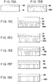
- Figs. 12A to 12E are schematic views for explaining one example of the production process of the present invention.
- Figs. 13A to 13E are schematic views for explaining one example of the production process of the present invention.
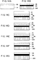
- Figs. 14A to 14G are schematic views for explaining one example of the production process of the present invention.
- Figs. 15A to 15G are schematic views for explaining one example of the production process of the present invention.
- the process for producing a semiconductor device substrate of the present invention comprises the steps of making a first substrate porous, forming an insulating layer on a second substrate, forming an amorphous layer on the insulating layer on the second substrate, bonding the porous first substrate to the amorphous layer at a temperature of an atmosphere in which the amorphous layer at least does not crystallize, causing solid-phase epitaxial growth of the amorphous layer by utilizing the porous first substrate as crystal growth seed, and removing the bonded first substrate after completion of the epitaxial growth.
- the process of the present invention is practicable by selectively chemical etching the porous Si without etching crystalline Si by use of a wet type chemical etching solution which does not adversely affect the semiconductor process.
- the selective etching of the porous Si in the present invention is conducted by use, as a selective etching solution having no etching action on crystal Si, of hydrofluoric acid or buffered hydrofluoric acid, or a mixture of hydrofluoric acid or buffered hydrofluoric acid with at least one of an alcohol and an aqueous hydroperoxide solution.
- monocrystalline Si is formed on different materials from it.
- selective etching is conducted in two steps in which the etching selectivity at the second step is extraordinarily high.
- the porous Si substrate formed on the first substrate member has pores of about 600 ⁇ in average diameter formed therein according to observation by transmission electron microscopy, and retains monocrystallinity in spite of the low density of half or less of the monocrystalline Si density. Therefore, a monocrystalline Si layer can be grown on the porous layer. At a temperature higher than 1000°C, however, the internal pores rearrange and the accelerated etching characteristics is impaired. Therefore, for epitaxial growth of the Si layer, low temperature growth methods such as molecular beam epitaxial growth, plasma CVD, low pressure CVD, photo-assisted CVD, bias sputtering and liquid phase growth methods are suitable.
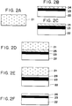
- an Si substrate 11 as a first substrate member shown in Fig. 1A is a P-type monocrystalline Si substrate. It is made porous as a whole.
- an insulating layer 13 and further thereon an amorphous Si layer 14 are formed.
- the porous structure of the Si substrate 11 is obtained by anodization in an HF solution.
- the density of the porous Si layer can be varied in the range of from 1.1 to 0.6 g/cm3 by varying the HF concentration from 50 % to 20 % in comparison with the density 2.33 g/cm3 of monocrystalline Si.
- This porous structure is not formed in an N-type Si layer, but is formed only in a P-type Si layer for the reason mentioned below.
- This porous Si layer has pores of about 600 ⁇ in average diameter according to observation by transmission electron microscopy.
- the porous layer has a density of half of or less than the density of the nonporous layer because of the large amount of void in the interior thereof, and has greater surface area for the volume. Consequently, the chemical etching rate of it is significantly greater than that of a normal monocrystalline layer.
- one face of the porous Si substrate 11 as the first substrate member is bonded to the face of the amorphous Si layer 14 of a second Si substrate member as shown in Fig. 1C.
- the bonded substrates are subjected to heat treatment at a temperature lower than the crystallization temperature of the amorphous Si, thereby the face of the porous Si 11 and the face of the amorphous Si 14 are bonded tightly.
- the bonded two substrate members are heat-treated to turn the amorphous Si 14 into a monocrystalline Si layer 15 by solid-phase epitaxial growth by utilizing the porous Si layer 11 as crystal-growth seed as shown in Fig. 1D. Since this solid-phase growth occurs in a vertical direction, the epitaxial growth is completed in a short time, and the crystal defects are considerably less than in lateral solid-phase epitaxial growth.
- the porous Si layer 11 only is removed by chemical etching while the monocrystalline Si left on the insulating layer 13.
- Fig. 1E shows the state after removal of the porous Si layer by etching. Thereby, the insulating layer 13 and the monocrystalline Si layer 15 is formed in a flat and uniform state, and over a large area of the entire wafer. The resulting semiconductor device substrate is excellent for insulation-separated electronic devices.
- Figs. 12A to 12E show examples in which a second substrate member 120 is made of a material different from Si.
- Figs. 13A to 13E show examples in which an insulating layer is not formed on a second substrate member 220.
- the porous Si can prevent the occurrence of defects.
- the porosity of Si is an important parameter for relaxation of strain caused by heteroepitaxial growth because of the nature of the porous structure. Therefore, the measurement of the porosity is indispensable.
- the known methods for the etching of porous Si include:
- a hydrofluoric nitric acid type etching solution is used normally. With this etching solution, the etching proceeds with oxidation of Si by nitric acid to form SiO2 and subsequent etching of the resulting SiO2 by hydrofluoric acid as shown below: Si + 2O ⁇ SiO2 (4) SiO2 + 4HF ⁇ SiF4 + 2H2O (5)
- the known methods for etching crystalline Si further include etching with an ethylenediamine type, KOH type, or hydrazine type of etching solution as well as the above hydrofluoric nitric acid type etching solution.
- an etching solution capable of etching the porous Si need to be selected from etching solutions other than the above Si-etching solutions.
- the selective etching of porous Si is conventionally conducted only by use of aqueous NaOH solution.
- hydrofluoric nitric acid type etching solution is used, not only amorphous Si but also crystalline Si is etched off.
- Fig. 4 shows the dependency of the etched layer thicknesses (thickness decreases) of porous Si and monocrystalline Si on etching time in the case where the porous Si and monocrystalline Si were respectively etched by immersion in buffered hydrofluoric acid (NH4F: 36 %, HF: 4.5 %) with stirring.
- the porous Si was prepared by anodization of monocrystalline Si under the conditions below.
- the starting material for the porous Si to be formed by the anodization is not limited to monocrystalline Si but any other crystal structure of Si may be employed.
- nonporous Si of 500 ⁇ m thick was etched by immersion in the buffered hydrofluoric acid with stirring at room temperature. The decrease of the thickness was measured later. The progress of the etching is shown by solid circles ( ⁇ ). The nonporous Si was etched by not more than 50 ⁇ even after 120 minutes.
- the porous Si and the nonporous Si were washed with water. The surfaces were observed by secondary ion mass spectrometry to detect no impurity.
- the conditions of the solution concentration and the temperature are decided within the range that the etching rate of the porous Si and the selectivity of the etching of the porous Si relative to nonporous Si are allowable in the production process, and the effect of the alcohol is achievable.
- Fig. 5 shows the dependency of the etched layer thicknesses (thickness decreases) of porous Si and monocrystalline Si on etching time in the case where the porous Si and monocrystalline Si were respectively etched by immersion in a 10:1 mixture of buffered hydrofluoric acid (NH4F: 36 %, HF: 4.5 %) and alcohol without stirring.
- the porous Si was prepared by anodization of monocrystalline Si under the conditions below.
- the starting material for the porous Si to be formed by the anodization is not limited to monocrystalline Si but any other crystal structure of Si may be employed.
- nonporous Si of 500 ⁇ m thick was etched by immersion in the 10:1 mixture of buffered hydrofluoric acid and alcohol at room temperature without stirring. The decrease of the thickness was measured later. The progress of the etching is shown by solid circles ( ⁇ ). The nonporous Si was etched by not more than 50 ⁇ even after 120 minutes of etching.
- the addition of alcohol allows the instantaneous removal of bubbles formed by the etching reaction from the etched surface without stirring, thus enabling uniform and effective etching of the porous Si.
- the porous Si and the nonporous Si were washed with water. The surfaces were observed by secondary ion mass spectrometry to detect no impurity.
- the conditions of the solution concentration and the temperature are decided within the range that the etching rate of the porous Si and the selectivity of the etching of the porous Si relative to nonporous Si are allowable in the production process, and the effect of the alcohol is achievable.
- Fig. 6 shows the dependency of the etched layer thicknesses (thickness decreases) of porous Si and monocrystalline Si on etching time in the case where the porous Si and monocrystalline Si were respectively etched by immersion in a 1:5 mixture of buffered hydrofluoric acid (NH4F: 36 %, HF: 4.5 %) and aqueous 30% hydrogen peroxide solution with stirring.
- the porous Si was prepared by anodization of monocrystalline Si under the conditions below.
- the starting material for the porous Si to be formed by the anodization is not limited to monocrystalline Si but any other crystal structure of Si may be employed.
- nonporous Si of 500 ⁇ m thick was etched by immersion in the 1:5 mixture of buffered hydrofluoric acid and aqueous 30% hydrogen peroxide solution at room temperature with stirring. The decrease of the thickness was measured later. The progress of the etching is shown by solid circles ( ⁇ ). The nonporous Si was etched by not more than 50 ⁇ even after 120 minutes of etching.
- the addition of the aqueous hydrogen peroxide solution accelerates the oxidation of silicon, and thereby accelerates the reaction velocity in comparison with the case of absence of hydrogen peroxide. Further the reaction velocity can be controlled by changing the ratio of the hydrogen peroxide solution.
- the porous Si and the nonporous Si were washed with water. The surfaces were observed by secondary ion mass spectrometry to detect no impurity.
- the conditions of the solution concentration and the temperature are decided within the range that the etching rate of the porous Si and the selectivity of the etching of the porous Si relative to nonporous Si are allowable in the production process, and the effect of the alcohol is achievable.
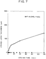
- Fig. 7 shows the dependency of the etched layer thicknesses (thickness decreases) of porous Si and monocrystalline Si on etching time in the case where the porous Si and monocrystalline Si were respectively etched by immersion in a 10:6:50 mixture of buffered hydrofluoric acid (NH4F: 36 %, HF: 4.5 %), alcohol and aqueous 30% hydrogen peroxide solution without stirring.
- the porous Si was prepared by anodization of monocrystalline Si under the conditions below.
- the starting material for the porous Si to be formed by the anodization is not limited to monocrystalline Si but any other crystal structure of Si may be employed.
- nonporous Si of 500 ⁇ m thick was etched by immersion in the 10:6:50 mixture of buffered hydrofluoric acid, alcohol and aqueous 30% hydrogen peroxide solution at room temperature without stirring. The decrease of the thickness was measured later. The progress of the etching is shown by solid circles ( ⁇ ). The nonporous Si was etched by not more than 50 ⁇ even after 120 minutes of etching.
- the addition of the aqueous hydrogen peroxide solution accelerates the oxidation of silicon, and thereby increases the reaction velocity in comparison with the case where hydrogen peroxide is absent. Further the reaction velocity can be controlled by changing the ratio of the hydrogen peroxide solution.
- the porous Si and the nonporous Si were washed with water. The surfaces were observed by secondary ion mass spectrometry to detect no impurity.
- the conditions of the solution concentration and the temperature are decided within the range that the etching rate of the porous Si and the selectivity of the etching of the porous Si relative to nonporous Si are allowable in the production process, and the effect of the alcohol is achievable.
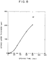
- Fig. 8 shows the dependency of the etched layer thicknesses (thickness decreases) of porous Si and monocrystalline Si on etching time in the case where the porous Si and monocrystalline Si were respectively etched by immersion in 49% hydrofluoric acid with stirring.
- the porous Si was prepared by anodization of monocrystalline Si under the conditions below.
- the starting material for the porous Si to be formed by the anodization is not limited to monocrystalline Si but any other crystal structure of Si may be employed.
- nonporous Si of 500 ⁇ m thick was etched by immersion in 49% hydrofluoric acid with stirring at room temperature. The decrease of the thickness was measured later. The progress of the etching is shown by solid circles ( ⁇ ). The nonporous Si was etched by not more than 50 ⁇ even after 80 minutes.
- the porous Si and the nonporous Si were washed with water. The surfaces were observed by secondary ion mass spectrometry to detect no impurity.
- the conditions of the solution concentration and the temperature are decided within the range that the etching rate of the porous Si and the selectivity of the etching of the porous Si relative to nonporous Si are allowable in the production process, and the effect of the alcohol is achievable.
- Fig. 9 shows the dependency of the etched layer thicknesses (thickness decreases) of porous Si and monocrystalline Si on etching time in the case where the porous Si and monocrystalline Si were respectively etched by immersion in a 10:1 mixture of 49% hydrofluoric acid and alcohol without stirring.
- the porous Si was prepared by anodization of monocrystalline Si under the conditions below.
- the starting material for the porous Si to be formed by the anodization is not limited to monocrystalline Si but any other crystal structure of Si may be employed.
- nonporous Si of 500 ⁇ m thick was etched by immersion in the 10:1 mixture of 49% hydrofluoric acid and alcohol at room temperature without stirring. The decrease of the thickness was measured later. The progress of the etching is shown by solid circles ( ⁇ ). The nonporous Si was etched by not more than 50 ⁇ even after 80 minutes of etching.
- the porous Si and the nonporous Si were washed with water. The surfaces were observed by secondary ion mass spectrometry to detect no impurity.
- the conditions of the solution concentration and the temperature are decided within the range that the etching rate of the porous Si and the selectivity of the etching of the porous Si relative to nonporous Si are allowable in the production process, and the effect of the alcohol is achievable.
- Fig. 10 shows the dependency of the etched layer thicknesses (thickness decreases) of porous Si and monocrystalline Si on etching time in the case where the porous Si and monocrystalline Si were respectively etched by immersion in a 1:5 mixture of 49% hydrofluoric acid and aqueous 30% hydrogen peroxide solution with stirring.
- the porous Si was prepared by anodization of monocrystalline Si under the conditions below.
- the starting material for the porous Si to be formed by the anodization is not limited to monocrystalline Si but any other crystal structure of Si may be employed.
- nonporous Si of 500 ⁇ m thick was etched by immersion in the 1:5 mixture of 49% hydrofluoric acid and aqueous 30% hydrogen peroxide solution at room temperature with stirring. The decrease of the thickness was measured later. The progress of the etching is shown by solid circles ( ⁇ ). The nonporous Si was etched by not more than 50 ⁇ even after 80 minutes of etching.
- the addition of the aqueous hydrogen peroxide solution accelerates the oxidation of silicon, and thereby increases the reaction velocity in comparison with the case of absence of hydrogen peroxide. Further the reaction velocity can be controlled by changing the ratio of the hydrogen peroxide solution.
- the porous Si and the nonporous Si were washed with water. The surfaces were observed by secondary ion mass spectrometry to detect no impurity.
- the conditions of the solution concentration and the temperature are decided within the range that the etching rate of the porous Si and the selectivity of the etching of the porous Si relative to nonporous Si are allowable in the production process, and the effect of the alcohol is achievable.
- Fig. 11 shows the dependency of the etched layer thicknesses (thickness decreases) of porous Si and monocrystalline Si on etching time in the case where the porous Si and monocrystalline Si were respectively etched by immersion in a 10:6:50 mixture of 49% hydrofluoric acid, alcohol and aqueous 30% hydrogen peroxide solution without stirring.
- the porous Si was prepared by anodization of monocrystalline Si under the conditions below.
- the starting material for the porous Si to be formed by the anodization is not limited to monocrystalline Si but any other crystal structure of Si may be employed.
- nonporous Si of 500 ⁇ m thick was etched by immersion in the 10:6:50 mixture of 49% hydrofluoric acid, alcohol and aqueous 30% hydrogen peroxide solution at room temperature without stirring. The decrease of the thickness was measured later. The progress of the etching is shown by solid circles ( ⁇ ). The nonporous Si was etched by not more than 50 ⁇ even after 80 minutes of etching.
- the addition of the aqueous hydrogen peroxide solution accelerates the oxidation of silicon, and thereby increases the reaction velocity in comparison with the case of absence of hydrogen peroxide. Further the reaction velocity can be controlled by changing the ratio of the hydrogen peroxide solution.
- the porous Si and the nonporous Si were washed with water. The surfaces were observed by secondary ion mass spectrometry to detect no impurity.
- the conditions of the solution concentration and the temperature are decided within the range that the etching rate of the porous Si and the selectivity of the etching of the porous Si relative to nonporous Si are allowable in the production process, and the effect of the alcohol is achievable.
- This Embodiment is different from the above Embodiment 1 in that on an Si substrate 22 as a second substrate member, an insulating layer 23 is formed, and further thereon a polycrystalline Si layer 24 is formed as shown in Fig. 2B, and subsequently the polycrystalline Si layer 24 is transformed into an amorphous layer 25 by ion implantation as shown in Fig. 2C.
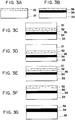
- the surface portion of a monocrystalline Si substrate 31 as a first substrate member is made porous to form a porous layer 32 as shown in Fig. 3A.
- a porous layer 32 On a second substrate member 33, an insulating layer 34 and further thereon an amorphous Si layer 35 are formed as shown in Fig. 3B.
- the inside wall of the pores of the porous layer 32 are allowed to be oxidized by spontaneous oxidation, oxidation with chemical in washing, thermal oxidation, etc.
- the porous layer 32 on the first substrate member and the amorphous layer 35 on the second substrate are bonded together as shown in Fig. 3C.
- the bonded article is heat-treated at a temperature lower than the crystallization temperature of the amorphous Si to bond tightly the face of the porous Si 32 and the face of the amorphous Si 35.
- the bonded substrate members are further heat-treated to form a monocrystalline Si layer 36 from the amorphous Si layer 35 by solid epitaxial growth by utilizing the porous Si layer 32 as the crystal growth seed as shown in Fig. 3D.
- the monocrystalline Si substrate 31 is removed by abrading and polishing to the extent that the porous Si layer 32 is just unexposed (Fig. 3E), and the remaining monocrystalline substrate 31 is removed by etching by utilizing the porous Si layer 32 as the etch-stop layer (first selective etching, Fig. 3F).
- first selective etching as an etching solution which etches Si more rapidly than SiO2, the etchant such as hydrofluoric nitric acid type etchants, a mixture of ethylenediamine, pyrocatechol and water, and KOH type etchants is used.
- the bonded substrate members in the step of Fig. 3F are chemically etched to remove the porous Si layer 32 (second selective etching), leaving the thin monocrystalline Si layer 36 on the insulating layer 34 (Fig. 3G).
- a monocrystalline Si substrate 31 as a first substrate member was made porous to form a porous layer 32 as shown in Fig. 14A.
- an insulating layer 34 and further thereon an amorphous Si layer 35 are formed as shown in Fig. 14B.
- the inside wall of the pores of the porous layer 32 are allowed to be oxidized by spontaneous oxidation, oxidation with a washing chemical, thermal oxidation, etc.
- the porous layer 32 on the first substrate member and the amorphous layer 35 on the second substrate are bonded together as shown in Fig. 14C.
- the bonded article is heat-treated at a temperature lower than the crystallization temperature of the amorphous Si to bond tightly the face of the porous Si 32 and the face of the amorphous Si 35.
- the monocrystalline Si substrate 31 is removed by abrading and polishing to the extent that the porous Si layer 32 is just unexposed (Fig. 14D).
- the bonded article is further heat-treated to form a monocrystalline Si layer 36 from the amorphous Si layer 35 by solid-phase epitaxial growth by utilizing the porous Si layer 32 as the crystal growth seed as shown in Fig. 14E.
- the remaining monocrystalline substrate 31 is removed by etching by utilizing the porous Si layer 32 as the etch-stop layer (first selective etching, Fig. 14F).
- first selective etching as an etching solution which etches Si more rapidly than SiO2 , the etchant such as hydrofluoric nitric acid type etchants, a mixture of ethylenediamine, pyrocatechol, and water, and KOH type etchants is used.
- the bonded substrates in the step of Fig. 14F are chemically etched to remove the porous Si layer 32 (second selective etching), leaving the thin monocrystalline Si layer 36 on the insulating layer 34 (Fig. 14G).
- no insulating layer is formed on the second substrate 430.
- the solid-phase epitaxial growth mentioned above may be conducted after the first selective etching.
- a monocrystalline Si substrate was anodized which has a thickness of 200 ⁇ m, a resistivity of 0.01 ⁇ cm, and crystal orientation (100), and was of P-type or N-type.
- the anodization conditions were as below.
- the bonded substrate members were heat-treated at 600°C for one hour so as to grow the amorphous Si by utilizing the porous Si as the crystal growth seed by solid-phase epitaxial growth. Thereby the amorphous Si layer entirely grew epitaxially in solid phase to form a monocrystalline Si film.
- the bonded substrate members were etched by immersion in a hydrofluoric acid-nitric acid-acetic acid (1:3:8) solution.
- the etching rate of the porous Si was about 100 times that of the monocrystalline Si owing to the reduced density by half and other reasons.
- the rate of etching of normal monocrystalline Si by the hydrofluoric acid-nitric acid-acetic acid (1:3:8) solution is 1 ⁇ m or a little less per minute. Therefore the porous Si region of 200 ⁇ m thick was removed in 2 minutes. Consequently, the porous Si substrate of 200 ⁇ m thick was removed, leaving a monocrystalline Si layer of 0.1 ⁇ m thick on the insulating substrate.
- the monocrystalline Si layer was found to have high crystallinity by observation of cross-section by transmission electron microscopy.
- Example 2 the solid-phase epitaxial growth was conducted at 1000°C for 5 minutes, while in Example 1 the heat treatment was conducted at 600°C for one hour.
- the etching of the porous Si of the bonded substrates was conducted in 7M NaOH solution.
- the porous Si region of 200 ⁇ m thick was removed in 2 minutes since the porous Si is etched more quickly than the monocrystalline Si and etching rate of the monocrystalline Si by 7M NaOH is 1 ⁇ m or a little less per minute.
- Other conditions such as the anodization conditions, and the amorphous Si deposition conditions, and the effects are the same as in Example 1. Therefore the description thereof is omitted here.
- the amorphous Si was treated at 1200°C for one minute according to RTA (rapid thermal annealing) method for solid-phase epitaxial growth thereof by utilizing the porous Si as the crystal growth seed.
- the bonded substrates were etched with 6M KOH solution. Thereby the porous Si region of 200 ⁇ m thick was removed in 2 minutes since the porous Si is etched more quickly than the monocrystalline Si and etching rate of the monocrystalline Si by 6M KOH is 1 ⁇ m or a little less per minute.
- Other conditions are the same as in Example 1, so that the description thereof is omitted here.
- an SiO2 layer of 500 nm thick was formed by thermal oxidation of the Si substrate, and further thereon an amorphous Si layer was deposited in a thickness of 0.1 ⁇ m by plasma CVD under the deposition conditions below.
- an SiO2 layer of 500 nm thick was formed by thermal oxidation of the Si substrate, and further on the SiO2 an amorphous Si layer was deposited in a thickness of 0.2 ⁇ m by vapor deposition under the deposition conditions below.
- Example 2 instead of directly forming an amorphous Si layer on an insulating layer on an Si substrate as the second substrate member, polycrystalline Si was deposited and then it was made amorphous.
- a monocrystalline Si substrate as a first substrate was made porous by anodization under the same conditions in Example 1.
- another Si substrate as a second substrate member was thermally oxidized to form thereon an SiO2 layer of 500 nm thick, and further thereon a polycrystalline Si layer was deposited in a thickness of 0.1 ⁇ m by thermal CVD under the deposition conditions below:
- the bonded substrate members were heat-treated at 600°C for one hour so as to grow the amorphous Si by utilizing the porous Si as the crystal growth seed by solid-phase epitaxial growth. Thereby the amorphous Si layer entirely grew epitaxially in solid phase to form a monocrystalline Si film.
- the bonded substrate members were etched in 7M NaOH solution.
- the etching rate of the porous Si was about 100 times that of the monocrystalline Si as mentioned before, and the rate of etching of normal monocrystalline Si by 7M NaOH solution is 1 ⁇ m or a little less per minute. Therefore the porous Si region of 200 ⁇ m thick was removed in 2 minutes. Consequently, the porous Si substrate of 200 ⁇ m thick was removed, leaving monocrystalline Si layer of 0.1 ⁇ m thick on the insulating substrate.
- the monocrystalline Si layer was found to have high crystallinity by observation of the cross-section by transmission electron microscopy.
- Example 6 the bonded substrate members in Example 6 were etched by immersion in 6M KOH solution.
- the etching rate of the porous Si was about 100 times that of the monocrystalline Si as mentioned before, and the rate of etching of normal monocrystalline Si by 6M KOH solution is 1 ⁇ m or a little less per minute. Therefore the porous Si region of 200 ⁇ m thick was removed in 2 minutes.
- Other conditions are the same as in Example 6, and are omitted here.
- Example 2 the deposition of amorphous Si on the insulating layer in Example 1 was conducted such that an SiO2 layer of 500 nm thick was formed on the Si substrate as the second substrate member by atmospheric pressure CVD. Further on the SiO2, an amorphous Si layer was deposited in a thickness of 0.2 ⁇ m by thermal CVD under the deposition conditions below:
- a P-type or N-type monocrystalline Si substrate was anodized which has a diameter of 6 inches, a thickness of 625 ⁇ m, a resistivity of 0.01 ⁇ cm, and crystal orientation (100).
- the anodization condition was as below.
- Another Si substrate as a second substrate member was thermally oxidized to form thereon an SiO2 layer of 500 nm thick, and further thereon a amorphous Si layer was deposited in a thickness of 0.1 ⁇ m by thermal CVD under the deposition conditions below:
- the surface of the porous Si and the surface of the amorphous Si were brought into contact, and the contacted article was heat-treated for 30 minutes at a temperature of 500°C which is lower than the crystallization temperature of the amorphous Si to complete the bonding.
- the bonded article was heat-treated at 600°C for 2 hours so as to grow the amorphous Si by utilizing the porous Si as the crystal growth seed by solid-phase epitaxial growth. Thereby the amorphous Si layer entirely grew epitaxially in solid phase to form a monocrystalline Si film.
- the first Si substrate was removed by grinding and polishing to leave a 10 ⁇ m-thick layer thereof remaining, and then this remaining 10 ⁇ m-thick monocrystalline Si substrate was selectively etched with a solution of "1 HF + 20 HNO3 + 20 CH3COOH" by utilizing the porous Si layer having pores oxidized at the internal walls as an etch-stop layer.
- the entire of the first Si substrate was etched in 10 minutes, whereby the porous Si layer came to be exposed.
- the bonded substrates were etched by immersion in a hydrofluoric acid-nitric acid-acetic acid (1:3:8) solution.
- the etching rate of the porous Si was about 100 times that of the monocrystalline Si as mentioned before.
- the rate of etching of normal monocrystalline Si in the hydrofluoric acid-nitric acid-acetic acid (1:3:8) solution is 1 ⁇ m or a little less per minute. Therefore the porous Si region of 10 ⁇ m thick was removed in 0.1 minute.
- the Si substrate of 625 ⁇ m thick was removed, leaving monocrystalline Si layer of 0.1 ⁇ m thick on the insulating substrate.
- the selective etching of the porous Si caused no change in the monocrystalline Si layer.
- the monocrystalline Si layer was found to have high crystallinity by observation of cross-section by transmission electron microscopy.
- This Example is different from Example 1 in the etching treatment after the monocrystalline Si layer was formed by solid-phase epitaxial growth.
- the bonded substrates were subjected to selective etching with a 10:6:50 mixture of buffered hydrofluoric acid (NH4F: 36%, HF: 4.5%), alcohol and aqueous 30% hydrogen peroxide solution without stirring.
- a 10:6:50 mixture of buffered hydrofluoric acid (NH4F: 36%, HF: 4.5%), alcohol and aqueous 30% hydrogen peroxide solution without stirring.
- the porous Si substrate was selectively removed completely with the monocrystalline Si left unetched as an etch-stop material.
- the rate of etching of the nonporous monocrystalline Si by the above etching solution is extremely low: about 50 ⁇ or less for 205 minutes. Therefore, the etching selectivity ratio of the porous Si to the nonporous Si is 105 or more, so that the layer thickness decrease of the nonporous layer (several tens of ⁇ ) by etching was practically negligible.
- This Example is different from Example 2 in the etching treatment after the monocrystalline Si layer was formed by solid-phase epitaxial growth.
- the bonded substrates were subjected to selective etching with a 1:5 mixture of buffered hydrofluoric acid (NH4F: 36%, HF: 4.5%) and aqueous 30% hydrogen peroxide solution with stirring. In 191 minutes, the porous Si substrate was selectively removed completely with the monocrystalline Si left unetched as an etch-stop material.
- the rate of etching of the nonporous monocrystalline Si by the above etching solution is extremely low: about 50 ⁇ or less for 191 minutes. Therefore, the etching selectivity ratio of the porous Si to the nonporous Si is 105 or more, so that the layer thickness decrease of the nonporous layer (several tens of ⁇ ) by etching was practically negligible.
- This Example is different from Example 3 in the etching treatment after the monocrystalline Si layer was formed by solid-phase epitaxial growth.
- the bonded substrates were subjected to selective etching with a 10:1 mixture of buffered hydrofluoric acid (NH4F: 36%, HF: 4.5%) and alcohol without stirring. In 275 minutes, the porous Si substrate was selectively removed completely with the monocrystalline Si left unetched as an etch-stop material.
- the rate of etching of the nonporous monocrystalline Si by the above etching solution is extremely low: about 50 ⁇ or less for 275 minutes. Therefore, the etching selectivity ratio of the porous Si to the nonporous Si is 105 or more, so that the layer thickness decrease of the nonporous layer (several tens of ⁇ ) by etching was practically negligible.
- This Example is different from Example 4 in the etching treatment after the monocrystalline Si layer was formed by solid-phase epitaxial growth.
- the bonded substrates were subjected to selective etching with buffered hydrofluoric acid (NH4F: 36%, HF: 4.5%) with stirring. In 258 minutes, the porous Si substrate was selectively removed completely with the monocrystalline Si left unetched as an etch-stop material.
- buffered hydrofluoric acid NHS: 36%, HF: 4.56%
- the rate of etching of the nonporous monocrystalline Si by the above etching solution is extremely low: about 50 ⁇ or less for 258 minutes. Therefore, the etching selectivity ratio of the porous Si to the nonporous Si is 105 or more, so that the layer thickness decrease of the nonporous layer (several tens of ⁇ ) by etching was practically negligible.
- This Example is different from Example 5 in the etching treatment after the monocrystalline Si layer was formed by solid-phase epitaxial growth.
- the bonded substrates were subjected to selective etching with a 10:6:50 mixture of buffered hydrofluoric acid (NH4F: 36%, HF: 4.5%), alcohol and aqueous 30% hydrogen peroxide solution without stirring.
- a 10:6:50 mixture of buffered hydrofluoric acid (NH4F: 36%, HF: 4.5%), alcohol and aqueous 30% hydrogen peroxide solution without stirring.
- the porous Si substrate was selectively removed completely with the monocrystalline Si left unetched as an etch-stop material.
- the rate of etching of the nonporous monocrystalline Si by the above etching solution is extremely low: about 50 ⁇ or less for 205 minutes. Therefore, the etching selectivity ratio of the porous Si to the nonporous Si is 105 or more, so that the layer thickness decrease of the nonporous layer (several tens of ⁇ ) by etching was is practically negligible.
- This Example is different from Example 6 in the etching treatment after the monocrystalline Si layer was formed by solid-phase epitaxial growth.
- the bonded substrates were subjected to selective etching with a 1:5 mixture of buffered hydrofluoric acid (NH4F: 36%, HF: 4.5%) and aqueous 30% hydrogen peroxide solution with stirring. In 191 minutes, the porous Si substrate was selectively removed completely with the monocrystalline Si left unetched as an etch-stop material.
- the rate of etching of the nonporous monocrystalline Si by the above etching solution is extremely low: about 50 ⁇ or less for 191 minutes. Therefore, the etching selectivity ratio of the porous Si to the nonporous Si is 105 or more, so that the layer thickness decrease of the nonporous layer (several tens of ⁇ ) by etching was practically negligible.
- This Example is different from Example 7 in the etching treatment after the monocrystalline Si layer was formed by solid-phase epitaxial growth.
- the bonded substrates were subjected to selective etching with a 10:1 mixture of buffered hydrofluoric acid (NH4F: 36%, HF: 4.5%) and alcohol without stirring. In 275 minutes, the porous Si substrate was selectively removed completely with the monocrystalline Si left unetched as an etch-stop material.
- the rate of etching of the nonporous monocrystalline Si by the above etching solution is extremely low: about 50 ⁇ or less for 275 minutes. Therefore, the etching selectivity ratio of the porous Si to the nonporous Si is 105 or more, so that the layer thickness decrease of the nonporous layer (several tens of ⁇ ) by etching was practically negligible.
- This Example is different from Example 8 in the etching treatment after the monocrystalline Si layer was formed by solid-phase epitaxial growth.
- the bonded substrates were subjected to selective etching with buffered hydrofluoric acid (NH4F: 36%, HF: 4.5%) with stirring. In 258 minutes, the porous Si substrate was selectively removed completely with the monocrystalline Si left unetched as an etch-stop material.
- buffered hydrofluoric acid NHS: 36%, HF: 4.56%
- the rate of etching of the nonporous monocrystalline Si by the above etching solution is extremely low: about 50 ⁇ or less for 258 minutes. Therefore, the etching selectivity ratio of the porous Si to the nonporous Si is 105 or more, so that the layer thickness decrease of the nonporous layer (several tens of ⁇ ) by etching was practically negligible.
- This Example is different from Example 9 in the etching treatment after the monocrystalline Si layer was formed by solid-phase epitaxial growth.
- the porous Si layer was selectively etched with a 1:5 mixture of buffered hydrofluoric acid (NH4F: 36%, HF: 4.5%) and aqueous 30% hydrogen peroxide solution with stirring. In one minute, the porous Si substrate was selectively removed completely with the monocrystalline Si left unetched as an etch-stop material.
- the rate of etching of the nonporous monocrystalline Si by the above etching solution is extremely low: about 50 ⁇ or less per minute. Therefore, the etching selectivity ratio of the porous Si to the nonporous Si is 105 or more, so that the layer thickness decrease of the nonporous layer (several tens of ⁇ ) by etching was practically negligible.
- This Example is different from Example 1 in the etching treatment after the monocrystalline Si layer was formed by solid-phase epitaxial growth.
- the bonded substrates were subjected to selective etching with a 10:6:50 mixture of 49 % hydrofluoric acid, alcohol and aqueous 30% hydrogen peroxide solution without stirring. In 65 minutes, the porous Si substrate was selectively removed completely with the monocrystalline Si left unetched as an etch-stop material.
- the rate of etching of the nonporous monocrystalline Si by the above etching solution is extremely low: about 50 ⁇ or less for 65 minutes. Therefore, the etching selectivity ratio of the porous Si to the nonporous Si is 105 or more, so that the layer thickness decrease of the nonporous layer (several tens of ⁇ ) by etching was practically negligible.
- This Example is different from Example 2 in the etching treatment after the monocrystalline Si layer was formed by solid-phase epitaxial growth.
- the bonded substrates were subjected to selective etching with a 1:5 mixture of 49 % hydrofluoric acid and aqueous 30% hydrogen peroxide solution with stirring. In 62 minutes, the porous Si substrate was selectively removed completely with the monocrystalline Si left unetched as an etch-stop material.
- the rate of etching of the nonporous monocrystalline Si by the above etching solution is extremely low: about 50 ⁇ or less for 62 minutes. Therefore, the etching selectivity ratio of the porous Si to the nonporous Si is 105 or more, so that the layer thickness decrease of the nonporous layer (several tens of ⁇ ) by etching was is practically negligible.
- This Example is different from Example 3 in the etching treatment after the monocrystalline Si layer was formed by solid-phase epitaxial growth.
- the bonded substrates were subjected to selective etching with a 10:1 mixture of 49 % hydrofluoric acid and alcohol without stirring. In 82 minutes, the porous Si substrate was selectively removed completely with the monocrystalline Si left unetched as an etch-stop material.
- the rate of etching of the nonporous monocrystalline Si by the above etching solution is extremely low: about 50 ⁇ or less for 82 minutes. Therefore, the etching selectivity ratio of the porous Si to the nonporous Si is 105 or more, so that the layer thickness decrease of the nonporous layer (several tens of ⁇ ) by etching was is practically negligible.
- This Example is different from Example 4 in the etching treatment after the monocrystalline Si layer was formed by solid-phase epitaxial growth.
- the bonded substrates were subjected to selective etching with 49% hydrofluoric acid with stirring. In 78 minutes, the porous Si substrate was selectively removed completely with the monocrystalline Si left unetched as an etch-stop material.
- the rate of etching of the nonporous monocrystalline Si by the above etching solution is extremely low: about 50 ⁇ or less for 78 minutes. Therefore, the etching selectivity ratio of the porous Si to the nonporous Si is 105 or more, so that the layer thickness decrease of the nonporous layer (several tens of ⁇ ) by etching was practically negligible.
- This Example is different from Example 5 in the etching treatment after the monocrystalline Si layer was formed by solid-phase epitaxial growth.
- the bonded substrates were subjected to selective etching with a 10:6:50 mixture of 49 % hydrofluoric acid, alcohol and aqueous 30% hydrogen peroxide solution without stirring. In 65 minutes, the porous Si substrate was selectively removed completely with the monocrystalline Si left unetched as an etch-stop material.
- the rate of etching of the nonporous monocrystalline Si by the above etching solution is extremely low: about 50 ⁇ or less for 65 minutes. Therefore, the etching selectivity ratio of the porous Si to the nonporous Si is 105 or more, so that the layer thickness decrease of the nonporous layer (several tens of ⁇ ) by etching was practically negligible.
- This Example is different from Example 6 in the etching treatment after the monocrystalline Si layer was formed by solid-phase epitaxial growth.
- the bonded substrates were subjected to selective etching with a 1:5 mixture of 49 % hydrofluoric acid and aqueous 30% hydrogen peroxide solution with stirring. In 62 minutes, the porous Si substrate was selectively removed completely with the monocrystalline Si left unetched as an etch-stop material.
- the rate of etching of the nonporous monocrystalline Si by the above etching solution is extremely low: about 50 ⁇ or less for 62 minutes. Therefore, the etching selectivity ratio of the porous Si to the nonporous Si is 105 or more, so that the layer thickness decrease of the nonporous layer (several tens of ⁇ ) by etching was practically negligible.
- This Example is different from Example 7 in the etching treatment after the monocrystalline Si layer was formed by solid-phase epitaxial growth.
- the bonded substrates were subjected to selective etching with a 10:1 mixture of 49 % hydrofluoric acid and alcohol without stirring. In 82 minutes, the porous Si substrate was selectively removed completely with the monocrystalline Si left unetched as an etch-stop material.
- the rate of etching of the nonporous monocrystalline Si by the above etching solution is extremely low: about 50 ⁇ or less for 82 minutes. Therefore, the etching selectivity ratio of the porous Si to the nonporous Si is 105 or more, so that the layer thickness decrease of the nonporous layer (several tens of ⁇ ) by etching was practically negligible.
- This Example is different from Example 8 in the etching treatment after the monocrystalline Si layer was formed by solid-phase epitaxial growth.
- the bonded substrates were subjected to selective etching with 49% hydrofluoric acid with stirring. In 78 minutes, the porous Si substrate was selectively removed completely with the monocrystalline Si left unetched as an etch-stop material.
- the rate of etching of the nonporous monocrystalline Si by the above etching solution is extremely low: about 50 ⁇ or less for 78 minutes. Therefore, the etching selectivity ratio of the porous Si to the nonporous Si is 105 or more, so that the layer thickness decrease of the nonporous layer (several tens of ⁇ ) by etching was practically negligible.
- This Example is different from Example 9 in the etching treatment after the monocrystalline Si layer was formed by solid-phase epitaxial growth.
- the bonded substrates were subjected to selective etching with a 1:5 mixture of 49 % hydrofluoric acid and aqueous 30% hydrogen peroxide solution with stirring. In 16.1 minutes, the porous Si substrate was selectively removed completely with the monocrystalline Si left unetched as an etch-stop material.
- the rate of etching of the nonporous monocrystalline Si by the above etching solution is extremely low: about 50 ⁇ or less for 16.1 minutes. Therefore, the etching selectivity ratio of the porous Si to the nonporous Si is 105 or more, so that the layer thickness decrease of the nonporous layer (several tens of ⁇ ) by etching was practically negligible.
- the materials of the first substrate member and the second substrate member are different from each other.
- a P-type or N-type (100) monocrystalline Si substrate having a thickness of 200 ⁇ m and resistivity of 0.01 ⁇ cm was employed as the first substrate member, and was anodized in an HF solution under the anodization conditions below:
- the bonded article was heat-treated at 600°C for one hour so as to grow the amorphous Si by utilizing the porous Si as the crystal growth seed by solid-phase epitaxial growth. Thereby the amorphous Si layer entirely grew epitaxially in a solid phase to form a monocrystalline Si film.
- an Si3N4 film was formed as an etching protection film, and the bonded article was selectively etched by immersion in a 10:6:50 mixture of 49 % hydrofluoric acid, alcohol and aqueous 30 % hydrogen peroxide solution without stirring. In 65 minutes, the porous Si substrate was selectively etched to completely remove with the monocrystalline Si left unetched as an etch-stop material.
- the rate of etching of the nonporous monocrystalline Si by the above etching solution is extremely low: about 50 ⁇ or less for 65 minutes. Therefore, the etching selectivity ratio of the porous Si to the nonporous Si is 105 or more, so that the layer thickness decrease of the nonporous layer (several tens of ⁇ ) by etching was is practically negligible.
- the porous Si substrate of 200 ⁇ m thick was removed, and after removal of the etching protection film, the monocrystalline Si layer of 0.1 ⁇ m thick was left on the light-transmissive substrate. No change was observed in the monocrystalline Si layer after the selective etching of the porous Si.
- the monocrystalline Si layer was found to have high crystallinity by observation of cross-section by transmission electron microscopy.
- a P-type or N-type (100) monocrystalline Si substrate having a thickness of 200 ⁇ m and resistivity of 0.01 ⁇ cm was employed as the first substrate member, and was anodized in an HF solution under the anodization conditions below:
- the bonded article was heat-treated at 700°C for 30 minutes so as to grow the amorphous Si by utilizing the porous Si as the crystal growth seed by solid-phase epitaxial growth, whereby the amorphous Si grew completely by solid-phase epitaxial growth to form a monocrystalline Si film.
- an Si3N4 film was formed as an etching protection film, and the bonded substrates were selectively etched in a 1:5 mixture of 49 % hydrofluoric acid and aqueous 30 % hydrogen peroxide solution with stirring. In 62 minutes, the porous Si substrate was selectively etched and completely removed with the monocrystalline Si left unetched as an etch-stop material.
- the rate of etching of the nonporous monocrystalline Si by the above etching solution is extremely low: about 50 ⁇ or less for 62 minutes. Therefore, the etching selectivity ratio of the porous Si to the nonporous Si is 105 or more, so that the layer thickness decrease of the nonporous layer (several tens of ⁇ ) by etching was practically negligible.
- the porous Si substrate of 200 ⁇ m thick was removed, and after removal of the etching protection film, the monocrystalline Si layer of 0.1 ⁇ m thick was left on the light-transmissive substrate. No change was observed in the monocrystalline Si layer after the selective etching of the porous Si.
- the monocrystalline Si layer was found to have high crystallinity by observation of cross-section by transmission electron microscopy.
- a P-type or N-type (100) monocrystalline Si substrate having a thickness of 200 ⁇ m and resistivity of 0.01 ⁇ cm was employed as the first substrate member, and was anodized in an HF solution under the anodization conditions below:
- the bonded article was heat-treated at 1200°C for 1 minute by RTA (rapid thermal annealing) for epitaxial growth of the amorphous Si by utilizing the porous Si as the seed, whereby the amorphous Si grew completely by solid-phase epitaxial growth to form a monocrystalline Si film.
- RTA rapid thermal annealing
- an Si3N4 film was formed as an etching protection film, and the bonded article was selectively etched by immersion in a hydrofluoric acid-nitric acid-acetic acid (1:3:8) solution. Since the rate of etching of porous Si is about 100 times that of monocrystalline Si as mentioned above and the rate of etching of normal monocrystalline Si is about 1 ⁇ m per minute, the amorphous Si region of 200 ⁇ m thick was removed in 2 minutes.
- the porous Si substrate of 200 ⁇ m thick was removed, and after removal of the etching protection film, the monocrystalline Si layer of 0.1 ⁇ m thick was left on the light-transmissive substrate. No change was observed in the monocrystalline Si layer after the selective etching of the porous Si.
- the monocrystalline Si layer was found to have high crystallinity by observation of cross-section by transmission electron microscopy.
- a P-type or N-type (100) monocrystalline Si substrate having a thickness of 525 ⁇ m, a diameter of 4 inches, and resistivity of 0.01 ⁇ cm was employed as the first substrate member, and was anodized in an HF solution under the anodization conditions below:
- an amorphous Si layer was deposited in a thickness of 0.1 ⁇ m by thermal CVD under the deposition conditions below:
- the bonded article was heat-treated at 600°C for one hour so as to grow the amorphous Si by utilizing the porous Si as the crystal growth seed by solid-phase epitaxial growth. Thereby the amorphous Si layer entirely grew epitaxially in a solid phase to form a monocrystalline Si film.
- the first Si substrate was removed by grinding and polishing, leaving a 10 ⁇ m-thick layer thereof remaining.
- the fused silica substrate side only of the bonded substrates was covered with Si3N4 as an etching protection film, and then this remaining 10 ⁇ m-thick monocrystalline Si substrate was selectively etched with a solution of "1 HF + 20 HNO3 + 20 CH3COOH" by utilizing the porous Si layer having pores oxidized at the internal walls as an etch-stop layer.
- the entire of the first Si substrate was etched in 10 minutes, thereby the porous Si layer coming to be exposed.
- the bonded article was selectively etched by 49 % hydrofluoric acid with stirring. In 18.6 minutes, the porous Si substrate was selectively etched and completely removed with the monocrystalline Si left unetched as the etch-stop material.
- the rate of etching of the nonporous monocrystalline Si by the above etching solution is extremely low: about 50 ⁇ or less for 18.6 minutes. Therefore, the etching selectivity ratio of the porous Si to the nonporous Si is 105 or more, so that the thickness decrease of the nonporous layer (several tens of ⁇ ) by etching was practically negligible.
- the Si substrate was removed, and after removal of the etching protection film, the monocrystalline Si layer of 0.1 ⁇ m thick was left on the light-transmissive substrate. No change was observed in the monocrystalline Si layer after the selective etching of the porous Si.
- the monocrystalline Si layer was found to have high crystallinity by observation of cross-section by transmission electron microscopy.
- a P-type or N-type (100) monocrystalline Si substrate having a thickness of 625 ⁇ m, a diameter of 5 inches, and resistivity of 0.01 ⁇ cm was employed as the first substrate member, and was anodized in an HF solution under the anodization conditions below:
- a polycrystalline Si layer was deposited in a thickness of 0.1 ⁇ m by thermal CVD under the deposition conditions below:
- the bonded article was heat-treated at 600°C for 2 hours so as to grow the amorphous Si by utilizing the porous Si as the crystal growth seed by solid-phase epitaxial growth. Thereby the amorphous Si layer entirely grew epitaxially in a solid phase to form a monocrystalline Si film.
- the first Si substrate was removed by grinding and polishing, leaving a 5 ⁇ m-thick layer thereof remaining. Only the fused silica substrate side of the bonded substrate members was covered with Si3N4 as an etching protection film, and the remaining monocrystalline Si substrate was selectively etched with a mixture of "ethylenediamine + pyrocatechol + water (mixing ratio of 17 ml : 3 g : 8 ml) at 110°C by utilizing the porous Si layer having pores oxidized at the internal walls as an etch-stop layer. The entire of the first Si substrate was etched in 3 minutes, whereby the whole porous Si layer region came to be exposed.
- the bonded substrates were selectively etched by a 10:6:50 mixture of 49 % hydrofluoric acid, alcohol and 30% hydrogen peroxide without stirring. In 11.4 minutes, the porous Si substrate was selectively etched and completely removed with the monocrystalline Si left unetched as the etch-stop material.
- the rate of etching of the nonporous monocrystalline Si by the above etching solution is extremely low: about 50 ⁇ or less for 11.4 minutes. Therefore, the etching selectivity ratio of the porous Si to the nonporous Si is 105 or more, so that the thickness decrease of the nonporous layer (several tens of ⁇ ) by etching was practically negligible.
- the Si substrate was removed, and after removal of the etching protection film, the monocrystalline Si layer of 0.1 ⁇ m thick was left on the light-transmissive substrate. No change was observed in the monocrystalline Si layer after the selective etching of the porous Si.
- the monocrystalline Si layer was found to have high crystallinity by observation of cross-section by transmission electron microscopy.
- a P-type or N-type (100) monocrystalline Si substrate having a thickness of 625 ⁇ m, a diameter of 6 inches, and resistivity of 0.01 ⁇ cm was employed as the first substrate member, and was anodized in an HF solution under the anodization conditions below:
- an amorphous Si layer was deposited in a thickness of 0.1 ⁇ m by thermal CVD under the deposition conditions below:
- the bonded article was heat-treated at 600°C for one hour so as to grow the amorphous Si by utilizing the porous Si as the crystal growth seed by solid-phase epitaxial growth. Thereby the amorphous Si layer entirely grew epitaxially in a solid phase to form a monocrystalline Si film.
- the first Si substrate was removed by grinding and polishing, leaving a 5 ⁇ m-thick layer thereof remaining.
- the fused silica substrate side only of the bonded substrates was covered with Si3N4 as an etching protection film, and the remaining monocrystalline Si substrate was selectively etched with aqueous 30% KOH solution at 110°C by utilizing the porous Si layer having pores oxidized at the internal walls as an etch-stop layer.
- the entire of the first Si substrate was etched in one minute, whereby the whole porous Si layer region came to be exposed.
- the bonded substrates were selectively etched by a 1:5 mixture of 49 % hydrofluoric acid and 30% hydrogen peroxide with stirring. In 11.1 minutes, the porous Si substrate was selectively etched and completely removed with the monocrystalline Si left unetched as the etch-stop material.
- the rate of etching of the nonporous monocrystalline Si by the above etching solution is extremely low: about 50 ⁇ or less for 11.1 minutes. Therefore, the etching selectivity ratio of the porous Si to the nonporous Si is 105 or more, so that the thickness decrease of the nonporous layer (several tens of ⁇ ) by etching was practically negligible.
- the Si substrate was removed, and after removal of the etching protection film, the monocrystalline Si layer of 0.1 ⁇ m thick was left on the light-transmissive substrate. No change was observed in the monocrystalline Si layer after the selective etching of the porous Si.
- the monocrystalline Si layer was found to have high crystallinity by observation of cross-section by transmission electron microscopy.
- a P-type or N-type (100) monocrystalline Si substrate having a thickness of 625 ⁇ m, a diameter of 6 inches, and resistivity of 0.01 ⁇ cm was employed as the first substrate member, and was anodized in an HF solution under the anodization conditions below:
- an Si3N4 layer of 100 nm thick, and further thereon an SiO2 layer of 500 nm thick were formed by CVD. Further on the SiO2 layer, an amorphous Si layer was deposited in a thickness of 0.1 ⁇ m by thermal CVD under the deposition conditions below:
- the bonded article was heat-treated at 600°C for one hour so as to grow the amorphous Si by utilizing the porous Si as the crystal growth seed by solid-phase epitaxial growth. Thereby the amorphous Si layer entirely grew epitaxially in a solid phase to form a monocrystalline Si film.
- the first Si substrate was removed by grinding and polishing, leaving a 10 ⁇ m-thick layer thereof remaining. Only the ceramic substrate side of the bonded substrates was covered with Si3N4 as an etching protection film, and the remaining monocrystalline Si substrate was selectively etched with a solution of "1 HF + 10 HNO3 + 10 CH3COOH" by utilizing the porous Si layer having pores oxidized at the internal walls as an etch-stop layer. The entire of the first Si substrate was etched in 5 minutes, whereby the porous Si layer came to be exposed.
- the bonded article was selectively etched by a 10:1 mixture of 49 % hydrofluoric acid and alcohol without stirring.
- the porous Si substrate was selectively etched and completely removed with the monocrystalline Si left unetched as the etch-stop material.
- the rate of etching of the nonporous monocrystalline Si by the above etching solution is extremely low: about 50 ⁇ or less for 12.7 minutes. Therefore, the etching selectivity ratio of the porous Si to the nonporous Si is 105 or more, so that the thickness decrease of the nonporous layer (several tens of ⁇ ) by etching was practically negligible.
- the Si substrate was removed, and after removal of the etching protection film, the monocrystalline Si layer of 0.1 ⁇ m thick was left on the ceramic substrate. No change was observed in the monocrystalline Si layer after the selective etching of the porous Si.
- the monocrystalline Si layer was found to have high crystallinity by observation of cross-section by transmission electron microscopy.
- Any substrate could be used in place of the ceramic substrate.
- a P-type or N-type (100) monocrystalline Si substrate having a thickness of 525 ⁇ m, a diameter of 4 inches, and resistivity of 0.01 ⁇ cm was employed as the first substrate member, and was anodized in an HF solution under the anodization conditions below:
- a CVD-SiO2 layer of 500 nm thick was formed on a fused silica substrate as the second substrate member. Further on the SiO2 layer, an amorphous Si layer was deposited in a thickness of 0.1 ⁇ m by thermal CVD under the deposition conditions below:
- the bonded article was heat-treated at 600°C for one hour so as to grow the amorphous Si by utilizing the porous Si as the crystal growth seed by solid-phase epitaxial growth. Thereby the amorphous Si layer entirely grew epitaxially in a solid phase to form a monocrystalline Si film.
- the bonded article was selectively etched by a 10:6:50 mixture of 49 % hydrofluoric acid, alcohol and aqueous 30% hydrogen peroxide without stirring.
- the porous Si substrate was selectively etched and completely removed with the monocrystalline Si left unetched as the etch-stop material.
- the rate of etching of the nonporous monocrystalline Si by the above etching solution is extremely low: about 50 ⁇ or less for 11.4 minutes. Therefore, the etching selectivity ratio of the porous Si to the nonporous Si is 105 or more, so that the thickness decrease of the nonporous layer (several tens of ⁇ ) by etching was practically negligible.
- the Si substrate was removed, and after removal of the etching protection film, the monocrystalline Si layer of 0.1 ⁇ m thick was left on the light-transmissive substrate. No change was observed in the monocrystalline Si layer after the selective etching of the porous Si.
- the monocrystalline Si layer was found to have high crystallinity by observation of cross-section by transmission electron microscopy.
- a P-type or N-type (100) monocrystalline Si substrate having a thickness of 625 ⁇ m, a diameter of 5 inches, and resistivity of 0.01 ⁇ cm was employed as the first substrate member, and was anodized in an HF solution under the anodization conditions below:
- an amorphous Si layer was deposited in a thickness of 0.1 ⁇ m by vapor deposition under the deposition conditions below:
- the glass substrate side only of the bonded substrates was covered with Si3N4 as an etching protection film, and the remaining 5 ⁇ m-thick monocrystalline Si substrate was selectively etched with a solution of "1 HF + 10 HNO3 + 10 CH3COOH" by utilizing the porous Si layer having pores oxidized at the internal walls as an etch-stop layer.
- the all of the first Si substrate was etched in 5 minutes, whereby the porous Si layer came to be exposed.
- the bonded article was heat-treated at 700°C for one hour so as to grow the amorphous Si by utilizing the porous Si as the crystal growth seed by solid-phase epitaxial growth. Thereby the amorphous Si layer entirely grew epitaxially in a solid phase to form a monocrystalline Si film.
- the bonded article was selectively etched by a 1:5 mixture of 49 % hydrofluoric acid and aqueous 30% hydrogen peroxide solution with stirring.
- the porous Si substrate was selectively etched and completely removed with the monocrystalline Si left unetched as the etch-stop material.
- the rate of etching of the nonporous monocrystalline Si by the above etching solution is extremely low: about 50 ⁇ or less for 16.1 minutes. Therefore, the etching selectivity ratio of the porous Si to the nonporous Si is 105 or more, so that the thickness decrease of the nonporous layer (several tens of ⁇ ) by etching was practically negligible.
- the Si substrate was removed, and after removal of the etching protection film, the monocrystalline Si layer of 0.1 ⁇ m thick was left on the light-transmissive substrate. No change was observed in the monocrystalline Si layer after the selective etching of the porous Si.
- the monocrystalline Si layer was found to have high crystallinity by observation of cross-section by transmission electron microscopy.
- a P-type or N-type (100) monocrystalline Si substrate having a thickness of 625 ⁇ m, a diameter of 6 inches, and resistivity of 0.01 ⁇ cm was employed as the first substrate member, and was anodized in an HF solution under the anodization conditions below:
- an amorphous Si layer was deposited in a thickness of 0.1 ⁇ m by bias sputtering under the deposition conditions below:
- the bonded article was heat-treated at 1200°C for one minute by RTA (rapid thermal annealing) so as to grow the amorphous Si by utilizing the porous Si as the crystal growth seed by solid-phase epitaxial growth. Thereby the amorphous Si layer entirely grew epitaxially in a solid phase to form a monocrystalline Si film.
- RTA rapid thermal annealing
- the fused silica substrate side only of the bonded substrates was covered with Si3N4 as an etching protection film, and the remaining 10 ⁇ m-thick monocrystalline Si substrate was selectively etched with a solution of "1 HF + 40 HNO3 + 40 CH3COOH" by utilizing the porous Si layer having pores oxidized at the internal walls as an etch-stop layer. All of the first Si substrate was etched in 15 minutes, whereby the porous Si layer came to be exposed.
- the bonded article was immersed in a hydrofluoric acid-nitric acid-acetic acid (1:3:8) solution.
- the rate of etching of porous Si is about 100 times that of monocrystalline Si, and the rate of etching of normal monocrystalline Si by the hydrofluoric acid-nitric acid-acetic acid (1:3:8) solution is about 1 ⁇ m per minute. Therefore, the porous Si substrate of 10 ⁇ m was removed within one minute.
- the Si substrate was removed, and after removal of the etching protection film, the monocrystalline Si layer of 0.1 ⁇ m thick was left on the light-transmissive substrate. No change was observed in the monocrystalline Si layer after the selective etching of the porous Si.
- the monocrystalline Si layer was found to have high crystallinity by observation of cross-section by transmission electron microscopy.
- a P-type or N-type (100) monocrystalline Si substrate having a thickness of 525 ⁇ m, a diameter of 4 inches, and resistivity of 0.01 ⁇ cm was employed as the first substrate member, and was anodized in an HF solution under the anodization conditions below:
- an amorphous Si layer was deposited in a thickness of 0.1 ⁇ m by thermal CVD under the deposition conditions below:
- the first Si substrate was removed by grinding and polishing, leaving a 10 ⁇ m-thick layer thereof remaining.
- the fused silica substrate side only of the bonded substrates was covered with Si3N4 as an etching protection film, and then the remaining 10 ⁇ m-thick monocrystalline Si substrate was selectively etched with a solution of "1 HF + 20 HNO3 + 20 CH3COOH" by utilizing the porous Si layer having pores oxidized at the internal walls as an etch-stop layer.
- the entire of the first Si substrate was etched in 10 minutes, whereby the porous Si layer came to be exposed.
- the bonded article was heat-treated at 600°C for one hour so as to grow the amorphous Si by utilizing the porous Si as the crystal growth seed by solid-phase epitaxial growth. Thereby the amorphous Si layer entirely grew epitaxially in a solid phase to form a monocrystalline Si film.
- the bonded article was selectively etched by 49 % hydrofluoric acid with stirring. In 18.6 minutes, the porous Si substrate was selectively etched and completely removed with the monocrystalline Si left unetched as the etch-stop material.
- the rate of etching of the nonporous monocrystalline Si by the above etching solution is extremely low: about 50 ⁇ or less for 18.6 minutes. Therefore, the etching selectivity ratio of the porous Si to the nonporous Si is 105 or more, so that the thickness decrease of the nonporous layer (several tens of ⁇ ) by etching was practically negligible.
- the Si substrate was removed, and after removal of the etching protection film, the monocrystalline Si layer of 0.1 ⁇ m thick was left on the light-transmissive substrate. No change was observed in the monocrystalline Si layer after the selective etching of the porous Si.
- the monocrystalline Si layer was found to have high crystallinity by observation of cross-section by transmission electron microscopy.
- a P-type or N-type (100) monocrystalline Si substrate having a thickness of 625 ⁇ m, a diameter of 5 inches, and resistivity of 0.01 ⁇ cm was employed as the first substrate member, and was anodized in an HF solution under the anodization conditions below:
- a polycrystalline Si layer was deposited in a thickness of 0.1 ⁇ m by thermal CVD under the deposition conditions below:
- the bonded article was heat-treated at 600°C for 2 hours so as to grow the amorphous Si by utilizing the porous Si as the crystal growth seed by solid-phase epitaxial growth. Thereby the amorphous Si layer entirely grew epitaxially in a solid phase to form a monocrystalline Si film.
- the fused silica substrate side only of the bonded substrate members was covered with Si3N4 as an etching protection film, and this remaining monocrystalline Si substrate was selectively etched with a mixture of "ethylenediamine + pyrocatechol + water (mixing ratio of 17 ml : 3 g : 8 ml) at 110°C by utilizing the porous Si layer having pores oxidized at the internal walls as an etch-stop layer.
- the entire of the first Si substrate was etched in 3 minutes, whereby the whole of the porous Si layer region came to be exposed.
- the bonded substrate members were selectively etched by a 10:6:50 mixture of 49 % hydrofluoric acid, alcohol and 30% hydrogen peroxide without stirring. In 11.4 minutes, the porous Si substrate was selectively etched and completely removed with the monocrystalline Si left unetched as the etch-stop material.
- the rate of etching of the nonporous monocrystalline Si by the above etching solution is extremely low: about 50 ⁇ or less for 11.4 minutes. Therefore, the etching selectivity ratio of the porous Si to the nonporous Si is 105 or more, so that the thickness decrease of the nonporous layer (several tens of ⁇ ) by etching was practically negligible.
- the Si substrate was removed, and after removal of the etching protection film, the monocrystalline Si layer of 0.1 ⁇ m thick was left on the light-transmissive substrate. No change was observed in the monocrystalline Si layer after the selective etching of the porous Si.
- the monocrystalline Si layer was found to have high crystallinity by observation of cross-section by transmission electron microscopy.
- a P-type or N-type (100) monocrystalline Si substrate having a thickness of 625 ⁇ m, a diameter of 6 inches, and resistivity of 0.01 ⁇ cm was employed as the first substrate member, and was anodized in an HF solution under the anodization conditions below:
- an amorphous Si layer was deposited in a thickness of 0.1 ⁇ m by thermal CVD under the deposition conditions below:
- the first Si substrate was removed by grinding and polishing, leaving a 5 ⁇ m-thick layer thereof remaining.
- the fused silica substrate side only of the bonded substrate members was covered with Si3N4 as an etching protection film, and this remaining monocrystalline Si substrate was selectively etched with aqueous 30% KOH solution at 110°C by utilizing the porous Si layer having pores oxidized at the inside walls as an etch-stop layer.
- the entire of the first Si substrate was etched in one minute, whereby the whole porous Si layer region came to be exposed.
- the bonded article was heat-treated at 600°C for one hour so as to grow the amorphous Si by utilizing the porous Si as the crystal growth seed by solid-phase epitaxial growth. Thereby the amorphous Si layer entirely grew epitaxially in a solid phase to form a monocrystalline Si film.
- the bonded article was selectively etched by a 1:5 mixture of 49 % hydrofluoric acid and 30% hydrogen peroxide with stirring. In 11.1 minutes, the porous Si substrate was selectively etched and completely removed with the monocrystalline Si left unetched as the etch-stop material.
- the rate of etching of the nonporous monocrystalline Si by the above etching solution is extremely low: about 50 ⁇ or less for 11.1 minutes. Therefore, the etching selectivity ratio of the porous Si to the nonporous Si is 105 or more, so that the thickness decrease of the nonporous layer (several tens of ⁇ ) by etching was practically negligible.
- the porous Si substrate was removed, and after removal of the etching protection film, the monocrystalline Si layer of 0.1 ⁇ m thick was left on the light-transmissive substrate. No change was observed in the monocrystalline Si layer after the selective etching of the porous Si.
- the monocrystalline Si layer was found to have high crystallinity by observation of cross-section by transmission electron microscopy.
- a P-type or N-type (100) monocrystalline Si substrate having a thickness of 625 ⁇ m, a diameter of 6 inches, and resistivity of 0.01 ⁇ cm was employed as the first substrate member, and was anodized in an HF solution under the anodization conditions below:
- an Si3N4 layer of 100 nm thick, and further thereon an SiO2 layer of 500 nm thick were formed by CVD. Further on the SiO2 layer, an amorphous Si layer was deposited in a thickness of 0.1 ⁇ m by thermal CVD under the deposition conditions below:
- the ceramic substrate side only of the bonded substrate members was covered with Si3N4 as an etching protection film. Then most of the first Si substrate was removed by etching with a solution of "66 HNO3 + 34 HF", leaving a 10 ⁇ m-thick layer thereof remaining. The remaining 10 ⁇ m-thick monocrystalline Si substrate was selectively etched with a solution of "1 HF + 10 HNO3 + 10 CH3COOH” by utilizing the porous Si layer having pores oxidized at the internal walls as an etch-stop layer. The entire of the first Si substrate was etched in 5 minutes, thereby the porous Si layer coming to be exposed.
- the bonded substrate members were heat-treated at 600°C for one hour so as to grow the amorphous Si by utilizing the porous Si as the crystal growth seed by solid-phase epitaxial growth. Thereby the amorphous Si layer entirely grew epitaxially in a solid phase to form a monocrystalline Si film.
- the bonded substrates were selectively etched by a 10:1 mixture of 49 % hydrofluoric acid and alcohol without stirring. In 12.7 minutes, the porous Si substrate was selectively etched and completely removed with the monocrystalline Si left unetched as the etch-stop material.
- the rate of etching of the nonporous monocrystalline Si by the above etching solution is extremely low: about 50 ⁇ or less for 12.7 minutes. Therefore, the etching selectivity ratio of the porous Si to the nonporous Si is 105 or more, so that the thickness decrease of the nonporous layer (several tens of ⁇ ) by etching was practically negligible.
- the porous Si substrate was removed, and after removal of the etching protection film, the monocrystalline Si layer of 0.1 ⁇ m thick was left on the ceramic substrate. No change was observed in the monocrystalline Si layer after the selective etching of the porous Si.
- the monocrystalline Si layer was found to have high crystallinity by observation of cross-section by transmission electron microscopy.
- Any substrate could be used in place of the ceramic substrate.
- a P-type or N-type (100) monocrystalline Si substrate having a thickness of 625 ⁇ m, a diameter of 5 inches, and resistivity of 0.01 ⁇ cm was employed as the first substrate member, and was anodized in an HF solution under the anodization conditions below:
- an amorphous GaAs layer was deposited in a thickness of 0.2 ⁇ m by MOCVD or MBE.
- the deposition was conducted under the deposition conditions employed generally in semiconductor processes.
- the surface of the porous Si and the surface of the amorphous GaAs were brought together into close contact, and the contacted article was heat-treated for 10 hours at a temperature of 200°C which is lower than the crystallization temperature of the amorphous GaAs to complete the bonding.
- the bonded article was heat-treated at 600°C for one hour so as to grow the amorphous GaAs by utilizing the porous Si as the crystal growth seed by solid-phase epitaxial growth. Thereby the amorphous GaAs layer entirely grew epitaxially in a solid phase to form a monocrystalline GaAs film.
- the fused silica substrate side only of the bonded substrate members were covered with Si3N4 as an etching protection film, and the remaining 10 ⁇ m-thick monocrystalline Si substrate was selectively etched with a solution of "1 HF + 20 HNO3 + 20 CH3COOH" by utilizing the porous Si layer having pores oxidized at the internal walls as an etch-stop layer.
- the all of the first substrate of Si was etched in 10 minutes, whereby the porous Si layer came to be exposed.
- the oxide film of the porous layer was removed by hydrofluoric acid. Thereafter the porous Si layer was etched by a mixture of ethylenediamine, pyrocatechol and water (mixing ratio of 17 ml : 3 g 8 ml) at 110 °C. In one minute, the porous Si was selectively etched and removed completely by utilizing the monocrystalline GaAs as the etch-stop material, with the monocrystalline GaAs remaining unetched.
- the rate of etching of the monocrystalline GaAs by the above etching solution is extremely low: about 50 ⁇ or less for 1 minute. Therefore, the thickness decrease of the GaAs layer (several tens of ⁇ ) by etching was practically negligible.
- the etching solution in this etching process is not limited to the one employed above. Any etching solution may be used which is capable of etching the porous Si and does not etch GaAs.
- the Si substrate was removed, and after the removal of the etching protection film, the monocrystalline GaAs layer of 0.1 ⁇ m thick was left on the light-transmissive substrate. No change was observed in the monocrystalline GaAs layer after the selective etching of the porous Si.
- the monocrystalline GaAs layer was found to have high crystallinity by observation of cross-section by transmission electron microscopy.
- the surface of a monocrystalline GaAs of 3 inches in diameter as a first substrate was made porous.
- an amorphous Si layer was deposited in a thickness of 0.1 ⁇ m by thermal CVD under the deposition conditions below:
- the bonded article was heat-treated at 600°C for one hour so as to grow the amorphous Si by utilizing the porous GaAs as the crystal growth seed by solid-phase epitaxial growth. Thereby the amorphous Si layer entirely grew epitaxially in a solid phase to form a monocrystalline Si film.
- the fused silica substrate side only of the bonded substrate members was covered with Si3N4 as an etching protection film, and the remaining monocrystalline GaAs substrate was etched with a mixture of "H2SO4 + H2O2 + H2O". Then by use of the same etching solution, porous GaAs layer was selectively etched. The porous GaAs was removed completely with the monocrystalline Si remaining as the etch-stop material.
- the etching solution in this etching process is not limited to the one employed above. Any etching solution may be used which is capable of etching the porous GaAs and does not etch monocrystalline Si.
- the GaAs substrate was removed, and after the removal of the etching protection film, the monocrystalline Si layer of 0.1 ⁇ m thick was left on the light-transmissive substrate. No change was observed in the monocrystalline Si layer after the selective etching of the porous GaAs.
- the monocrystalline Si layer was found to have high crystallinity by observation of cross-section by transmission electron microscopy.
- the present invention provides a process for producing semiconductor device substrate which has solved the above-mentioned problems.
- the present invention provides a process for forming a monocrystalline Si layer with high crystallinity on an insulating substrate, which is advantageous in productivity, uniformity, controllability, and cost.
- the present provides a semiconductor device substrate which is applicable for conventional SOI device and realizes the advantage of the SOI.
- the present invention provides a process for producing a semiconductor device substrate which is useful in place of expensive SOS and SIMOX in production of large scale integrated circuits of SOI structure.
- a monocrystalline Si layer is formed by transforming a monocrystalline Si substrate of originally high quality into porous Si which is removable selectively and by growing an amorphous Si layer formed on an insulating layer through solid-phase epitaxial growth to form a monocrystalline Si layer while utilizing the resulting porous monocrystalline Si as a crystal growth seed.
- the amorphous Si on an insulating layer is grown in a vertical direction through solid-phase epitaxial growth. Therefore, the required growth length is only the thickness of amorphous Si layer, so that the growth is completed in a short time, and the crystallinity of the film is greatly improved in comparison with lateral solid-phase epitaxial growth which is practiced in production of SOI. Moreover, the present process enables formation of a solid-phase epitaxial monocrystalline layer over the whole face of a wafer, which gives great improvement in productivity and economics.
- a buffered hydrofluoric acid type of wet chemical etching solution may be used which does not adversely affect the semiconductor process, and the etching selectivity ratio of the porous Si to the nonporous Si is more than 105, which gives great advance in controllability and productivity.
- a buffered hydrofluoric acid type of wet chemical etching solution may also be used which does not adversely affect the semiconductor process, and the etching selectivity ratio of the porous Si to the nonporous Si is more than 105, which gives great advance in controllability and productivity.
- the present invention provides an excellent process for producing a monocrystalline Si layer with high crystallinity on an light-transmissive substrate by use of a light-transmissive substrate of a different kind of material, which is advantageous in productivity, uniformity, controllability, and economics.
- This process enables formation of a high-performance driving element on a monocrystalline Si, thereby giving a sensor or image elements (picture elements) of a displaying device with higher density, higher resolution and higher fineness.
- the present invention enables formation of three-dimensional structure in combination with another functional device, or enables use of a material other than Si as a substrate which has properties not achievable with Si, such as light-transmissivity, high heat releasability, high mechanical strength, and low cost.
- the amorphous Si is grown on a substrate made of another kind of material in a vertical direction through solid-phase epitaxial growth. Therefore, the required growth length is only the thickness of amorphous Si layer, so that the growth is completed in a short time, and the crystallinity of the film is greatly improved in comparison with lateral solid-phase epitaxial growth which is practiced in production of SOI. Moreover, the present process enables formation of solid-phase epitaxial monocrystalline layer over the whole face of a wafer, which gives great improvement in productivity and economics.
- an Si substrate is made thin by grinding and polishing before solid epitaxial growth whereby peeling or breaking of bonded substrates is avoided in the solid-phase growth at a temperature higher than the solid-phase growth temperature, even when different substrates having different thermal expansion coefficients is bonded.
- the process for producing a semiconductor device substrate of the present invention gives a uniform flat monocrystalline Si having extremely high crystallinity over a large area by employing two-step selective etching in which the selectivity in the second etching step is remarkably high.
- the oxidation of the internal wall of the pores of porous Si is known to be effective in inhibiting structural change of the porous Si during heat treatment. Further effects are achieved in the present invention in (1) improvement of the selectivity at the first etching step, and (2) acceleration of etching of porous Si in the second etching step to give a high selectivity.
- the porous Si layer serves as a satisfactory etch-stop layer by use of an etching solution exhibiting a higher etching velocity to Si than to SiO2.
- the exposed porous Si region which comes to be exposed earlier owing to non-uniformity of the porous Si thickness and irregularity of etching of the first etching step will become thin before the completion of etching of the bulk Si in other region.
- the extraordinary high selectivity in the second etching step compensates the nonuniformity of the thickness of the remaining porous Si.
- a process for producing a semiconductor device substrate comprises the steps of making a first substrate member porous, forming an insulating layer on a second substrate member, forming an amorphous layer on the insulating layer on the second substrate member, bonding the porous first substrate member to the amorphous layer at a temperature of an atmosphere in which the amorphous layer at least does not crystallize, causing solid-phase epitaxial growth of the amorphous layer by utilizing the porous first substrate member as crystal growth seed, and removing the bonded first substrate member after completion of the epitaxial growth by chemical etching.
Landscapes
- Recrystallisation Techniques (AREA)
Applications Claiming Priority (3)
| Application Number | Priority Date | Filing Date | Title |
|---|---|---|---|
| JP04630792A JP3250673B2 (ja) | 1992-01-31 | 1992-01-31 | 半導体素子基体とその作製方法 |
| JP46307/92 | 1992-01-31 | ||
| JP4630792 | 1992-01-31 |
Publications (3)
| Publication Number | Publication Date |
|---|---|
| EP0553855A2 true EP0553855A2 (fr) | 1993-08-04 |
| EP0553855A3 EP0553855A3 (en) | 1997-09-10 |
| EP0553855B1 EP0553855B1 (fr) | 2003-11-12 |
Family
ID=12743539
Family Applications (1)
| Application Number | Title | Priority Date | Filing Date |
|---|---|---|---|
| EP93101416A Expired - Lifetime EP0553855B1 (fr) | 1992-01-31 | 1993-01-29 | Dispositif semi-conducteur et procédé de sa fabrication |
Country Status (4)
| Country | Link |
|---|---|
| US (1) | US5492859A (fr) |
| EP (1) | EP0553855B1 (fr) |
| JP (1) | JP3250673B2 (fr) |
| DE (1) | DE69333294T2 (fr) |
Cited By (4)
| Publication number | Priority date | Publication date | Assignee | Title |
|---|---|---|---|---|
| EP0553856A3 (en) * | 1992-01-31 | 1997-10-01 | Canon Kk | Semiconductor substrate and method for preparing same |
| EP1926132A1 (fr) * | 2006-11-23 | 2008-05-28 | S.O.I.Tec Silicon on Insulator Technologies | Solution de gravure sans chrome pour substrats Si et SiGe, procédé de révélation de défauts et procédé de traitement de substrats Si ou SiGe |
| EP1956643A1 (fr) * | 2007-02-07 | 2008-08-13 | Siltronic AG | Procédé de réduction et d'homogénéisation de l'épaisseur d'une couche semi-conductrice, qui se trouve sur la surface d'un matériau électriquement isolant |
| EP3109894A4 (fr) * | 2014-02-18 | 2017-11-08 | NGK Insulators, Ltd. | Substrat de manipulation de substrat composite pour semi-conducteur et substrat composite pour semi-conducteur |
Families Citing this family (77)
| Publication number | Priority date | Publication date | Assignee | Title |
|---|---|---|---|---|
| SG93197A1 (en) * | 1991-02-15 | 2002-12-17 | Canon Kk | Etching solution for etching porous silicon, etching method using the etching solution and method of preparing semiconductor member using the etching solution |
| US6004865A (en) * | 1993-09-06 | 1999-12-21 | Hitachi, Ltd. | Method of fabricating multi-layered structure having single crystalline semiconductor film formed on insulator |
| JP3250721B2 (ja) * | 1995-12-12 | 2002-01-28 | キヤノン株式会社 | Soi基板の製造方法 |
| FR2748851B1 (fr) * | 1996-05-15 | 1998-08-07 | Commissariat Energie Atomique | Procede de realisation d'une couche mince de materiau semiconducteur |
| US6054363A (en) * | 1996-11-15 | 2000-04-25 | Canon Kabushiki Kaisha | Method of manufacturing semiconductor article |
| EP0849788B1 (fr) * | 1996-12-18 | 2004-03-10 | Canon Kabushiki Kaisha | Procédé de fabrication d'un article semiconducteur utilisant un substrat ayant une couche d'un semiconducteur poreux |
| EP0851513B1 (fr) * | 1996-12-27 | 2007-11-21 | Canon Kabushiki Kaisha | Méthode de fabrication d'un composant semiconducteur et méthode de fabrication d'une cellule solaire |
| US6756289B1 (en) | 1996-12-27 | 2004-06-29 | Canon Kabushiki Kaisha | Method of producing semiconductor member and method of producing solar cell |
| RU2125323C1 (ru) * | 1997-03-06 | 1999-01-20 | Институт физики полупроводников СО РАН | Способ получения структуры "полупроводник-на-изоляторе" |
| US6143628A (en) * | 1997-03-27 | 2000-11-07 | Canon Kabushiki Kaisha | Semiconductor substrate and method of manufacturing the same |
| JP3985065B2 (ja) | 1997-05-14 | 2007-10-03 | 忠弘 大見 | 多孔質シリコン基板の形成方法及び多孔質シリコン基板の形成装置 |
| EP0895282A3 (fr) | 1997-07-30 | 2000-01-26 | Canon Kabushiki Kaisha | Méthode de fabrication d'un substrat du type SOI utilisant un procédé de bonding, et substrat SOI fabriqué par ce procédé |
| DE19803013B4 (de) * | 1998-01-27 | 2005-02-03 | Robert Bosch Gmbh | Verfahren zum Ablösen einer Epitaxieschicht oder eines Schichtsystems und nachfolgendem Aufbringen auf einen alternativen Träger |
| TW469643B (en) * | 1998-09-04 | 2001-12-21 | Canon Kk | Process for producing semiconductor substrate |
| JP3903215B2 (ja) * | 1998-11-24 | 2007-04-11 | ダイキン工業株式会社 | エッチング液 |
| US6080683A (en) * | 1999-03-22 | 2000-06-27 | Special Materials Research And Technology, Inc. | Room temperature wet chemical growth process of SiO based oxides on silicon |
| US6593077B2 (en) | 1999-03-22 | 2003-07-15 | Special Materials Research And Technology, Inc. | Method of making thin films dielectrics using a process for room temperature wet chemical growth of SiO based oxides on a substrate |
| US6693033B2 (en) | 2000-02-10 | 2004-02-17 | Motorola, Inc. | Method of removing an amorphous oxide from a monocrystalline surface |
| US6392257B1 (en) * | 2000-02-10 | 2002-05-21 | Motorola Inc. | Semiconductor structure, semiconductor device, communicating device, integrated circuit, and process for fabricating the same |
| US6858462B2 (en) * | 2000-04-11 | 2005-02-22 | Gratings, Inc. | Enhanced light absorption of solar cells and photodetectors by diffraction |
| KR20030011083A (ko) * | 2000-05-31 | 2003-02-06 | 모토로라 인코포레이티드 | 반도체 디바이스 및 이를 제조하기 위한 방법 |
| US6501973B1 (en) | 2000-06-30 | 2002-12-31 | Motorola, Inc. | Apparatus and method for measuring selected physical condition of an animate subject |
| US6555946B1 (en) | 2000-07-24 | 2003-04-29 | Motorola, Inc. | Acoustic wave device and process for forming the same |
| US6590236B1 (en) | 2000-07-24 | 2003-07-08 | Motorola, Inc. | Semiconductor structure for use with high-frequency signals |
| AU2001277001A1 (en) * | 2000-07-24 | 2002-02-05 | Motorola, Inc. | Heterojunction tunneling diodes and process for fabricating same |
| US6493497B1 (en) | 2000-09-26 | 2002-12-10 | Motorola, Inc. | Electro-optic structure and process for fabricating same |
| US6638838B1 (en) | 2000-10-02 | 2003-10-28 | Motorola, Inc. | Semiconductor structure including a partially annealed layer and method of forming the same |
| US6559471B2 (en) | 2000-12-08 | 2003-05-06 | Motorola, Inc. | Quantum well infrared photodetector and method for fabricating same |
| JP4511092B2 (ja) * | 2000-12-11 | 2010-07-28 | セイコーエプソン株式会社 | 半導体素子の製造方法 |
| KR20020060457A (ko) * | 2001-01-11 | 2002-07-18 | 송오성 | 에스오아이 기판의 제조방법 |
| US20020096683A1 (en) * | 2001-01-19 | 2002-07-25 | Motorola, Inc. | Structure and method for fabricating GaN devices utilizing the formation of a compliant substrate |
| US6673646B2 (en) | 2001-02-28 | 2004-01-06 | Motorola, Inc. | Growth of compound semiconductor structures on patterned oxide films and process for fabricating same |
| WO2002082551A1 (fr) | 2001-04-02 | 2002-10-17 | Motorola, Inc. | Structure de semi-conducteur a courant de fuite attenue |
| US6709989B2 (en) | 2001-06-21 | 2004-03-23 | Motorola, Inc. | Method for fabricating a semiconductor structure including a metal oxide interface with silicon |
| US6613697B1 (en) | 2001-06-26 | 2003-09-02 | Special Materials Research And Technology, Inc. | Low metallic impurity SiO based thin film dielectrics on semiconductor substrates using a room temperature wet chemical growth process, method and applications thereof |
| US6992321B2 (en) | 2001-07-13 | 2006-01-31 | Motorola, Inc. | Structure and method for fabricating semiconductor structures and devices utilizing piezoelectric materials |
| US20030010992A1 (en) * | 2001-07-16 | 2003-01-16 | Motorola, Inc. | Semiconductor structure and method for implementing cross-point switch functionality |
| US6531740B2 (en) | 2001-07-17 | 2003-03-11 | Motorola, Inc. | Integrated impedance matching and stability network |
| US6646293B2 (en) | 2001-07-18 | 2003-11-11 | Motorola, Inc. | Structure for fabricating high electron mobility transistors utilizing the formation of complaint substrates |
| US7019332B2 (en) | 2001-07-20 | 2006-03-28 | Freescale Semiconductor, Inc. | Fabrication of a wavelength locker within a semiconductor structure |
| US6693298B2 (en) | 2001-07-20 | 2004-02-17 | Motorola, Inc. | Structure and method for fabricating epitaxial semiconductor on insulator (SOI) structures and devices utilizing the formation of a compliant substrate for materials used to form same |
| US6855992B2 (en) * | 2001-07-24 | 2005-02-15 | Motorola Inc. | Structure and method for fabricating configurable transistor devices utilizing the formation of a compliant substrate for materials used to form the same |
| US6585424B2 (en) | 2001-07-25 | 2003-07-01 | Motorola, Inc. | Structure and method for fabricating an electro-rheological lens |
| US6667196B2 (en) | 2001-07-25 | 2003-12-23 | Motorola, Inc. | Method for real-time monitoring and controlling perovskite oxide film growth and semiconductor structure formed using the method |
| US6594414B2 (en) | 2001-07-25 | 2003-07-15 | Motorola, Inc. | Structure and method of fabrication for an optical switch |
| US6589856B2 (en) | 2001-08-06 | 2003-07-08 | Motorola, Inc. | Method and apparatus for controlling anti-phase domains in semiconductor structures and devices |
| US6639249B2 (en) | 2001-08-06 | 2003-10-28 | Motorola, Inc. | Structure and method for fabrication for a solid-state lighting device |
| US20030034491A1 (en) | 2001-08-14 | 2003-02-20 | Motorola, Inc. | Structure and method for fabricating semiconductor structures and devices for detecting an object |
| US6673667B2 (en) | 2001-08-15 | 2004-01-06 | Motorola, Inc. | Method for manufacturing a substantially integral monolithic apparatus including a plurality of semiconductor materials |
| US20030036217A1 (en) * | 2001-08-16 | 2003-02-20 | Motorola, Inc. | Microcavity semiconductor laser coupled to a waveguide |
| KR20030032133A (ko) * | 2001-10-10 | 2003-04-26 | 유종훈 | 비정질실리콘 박막층이 증착된 다공질실리콘 반도체의제조방법 |
| US20030071327A1 (en) * | 2001-10-17 | 2003-04-17 | Motorola, Inc. | Method and apparatus utilizing monocrystalline insulator |
| KR20030064536A (ko) * | 2002-01-28 | 2003-08-02 | 텔레포스 주식회사 | 산화된 다공성 실리콘층을 이용한 고주파 소자 |
| US6916717B2 (en) | 2002-05-03 | 2005-07-12 | Motorola, Inc. | Method for growing a monocrystalline oxide layer and for fabricating a semiconductor device on a monocrystalline substrate |
| KR100475077B1 (ko) * | 2002-05-31 | 2005-03-10 | 삼성전자주식회사 | 캐패시터의 유전막 형성방법 |
| US20040012037A1 (en) * | 2002-07-18 | 2004-01-22 | Motorola, Inc. | Hetero-integration of semiconductor materials on silicon |
| US20040070312A1 (en) * | 2002-10-10 | 2004-04-15 | Motorola, Inc. | Integrated circuit and process for fabricating the same |
| US20040069991A1 (en) * | 2002-10-10 | 2004-04-15 | Motorola, Inc. | Perovskite cuprate electronic device structure and process |
| US7169619B2 (en) | 2002-11-19 | 2007-01-30 | Freescale Semiconductor, Inc. | Method for fabricating semiconductor structures on vicinal substrates using a low temperature, low pressure, alkaline earth metal-rich process |
| US6885065B2 (en) | 2002-11-20 | 2005-04-26 | Freescale Semiconductor, Inc. | Ferromagnetic semiconductor structure and method for forming the same |
| US7020374B2 (en) * | 2003-02-03 | 2006-03-28 | Freescale Semiconductor, Inc. | Optical waveguide structure and method for fabricating the same |
| US6965128B2 (en) * | 2003-02-03 | 2005-11-15 | Freescale Semiconductor, Inc. | Structure and method for fabricating semiconductor microresonator devices |
| US20040164315A1 (en) * | 2003-02-25 | 2004-08-26 | Motorola, Inc. | Structure and device including a tunneling piezoelectric switch and method of forming same |
| US7592239B2 (en) | 2003-04-30 | 2009-09-22 | Industry University Cooperation Foundation-Hanyang University | Flexible single-crystal film and method of manufacturing the same |
| JP4959552B2 (ja) * | 2004-04-28 | 2012-06-27 | アイユーシーエフ‐エイチワイユー | 可撓性単結晶フィルム及びその製造方法 |
| KR20060081296A (ko) * | 2005-01-08 | 2006-07-12 | 삼성코닝 주식회사 | 실리콘 필름의 제조방법 |
| FR2886051B1 (fr) * | 2005-05-20 | 2007-08-10 | Commissariat Energie Atomique | Procede de detachement d'un film mince |
| US20070111468A1 (en) * | 2005-07-19 | 2007-05-17 | The Regents Of The University Of California | Method for fabricating dislocation-free stressed thin films |
| US8871610B2 (en) * | 2008-10-02 | 2014-10-28 | Semiconductor Energy Laboratory Co., Ltd. | Method for manufacturing SOI substrate |
| FR2938120B1 (fr) * | 2008-10-31 | 2011-04-08 | Commissariat Energie Atomique | Procede de formation d'une couche monocristalline dans le domaine micro-electronique |
| FR2938117B1 (fr) * | 2008-10-31 | 2011-04-15 | Commissariat Energie Atomique | Procede d'elaboration d'un substrat hybride ayant une couche continue electriquement isolante enterree |
| JP5158807B2 (ja) * | 2009-02-10 | 2013-03-06 | 独立行政法人産業技術総合研究所 | 光電変換素子およびその製造方法 |
| FR2953640B1 (fr) | 2009-12-04 | 2012-02-10 | S O I Tec Silicon On Insulator Tech | Procede de fabrication d'une structure de type semi-conducteur sur isolant, a pertes electriques diminuees et structure correspondante |
| US9287353B2 (en) * | 2010-11-30 | 2016-03-15 | Kyocera Corporation | Composite substrate and method of manufacturing the same |
| US11664357B2 (en) * | 2018-07-03 | 2023-05-30 | Adeia Semiconductor Bonding Technologies Inc. | Techniques for joining dissimilar materials in microelectronics |
| US10553474B1 (en) * | 2018-08-29 | 2020-02-04 | Taiwan Semiconductor Manufacturing Co., Ltd. | Method for forming a semiconductor-on-insulator (SOI) substrate |
| US11232974B2 (en) | 2018-11-30 | 2022-01-25 | Taiwan Semiconductor Manufacturing Company, Ltd. | Fabrication method of metal-free SOI wafer |
Family Cites Families (10)
| Publication number | Priority date | Publication date | Assignee | Title |
|---|---|---|---|---|
| US3929529A (en) * | 1974-12-09 | 1975-12-30 | Ibm | Method for gettering contaminants in monocrystalline silicon |
| US4628591A (en) * | 1984-10-31 | 1986-12-16 | Texas Instruments Incorporated | Method for obtaining full oxide isolation of epitaxial islands in silicon utilizing selective oxidation of porous silicon |
| JPH0624231B2 (ja) * | 1985-06-13 | 1994-03-30 | 沖電気工業株式会社 | 半導体装置の製造方法 |
| FR2620571B1 (fr) * | 1987-09-11 | 1990-01-12 | France Etat | Procede de fabrication d'une structure de silicium sur isolant |
| US5147808A (en) * | 1988-11-02 | 1992-09-15 | Universal Energy Systems, Inc. | High energy ion implanted silicon on insulator structure |
| US5094697A (en) * | 1989-06-16 | 1992-03-10 | Canon Kabushiki Kaisha | Photovoltaic device and method for producing the same |
| US5013681A (en) * | 1989-09-29 | 1991-05-07 | The United States Of America As Represented By The Secretary Of The Navy | Method of producing a thin silicon-on-insulator layer |
| SG59963A1 (en) * | 1990-08-03 | 1999-02-22 | Canon Kk | Semiconductor member and process for preparing semiconductor member |
| US5240876A (en) * | 1991-02-22 | 1993-08-31 | Harris Corporation | Method of fabricating SOI wafer with SiGe as an etchback film in a BESOI process |
| JP3112106B2 (ja) * | 1991-10-11 | 2000-11-27 | キヤノン株式会社 | 半導体基材の作製方法 |
-
1992
- 1992-01-31 JP JP04630792A patent/JP3250673B2/ja not_active Expired - Fee Related
-
1993
- 1993-01-29 EP EP93101416A patent/EP0553855B1/fr not_active Expired - Lifetime
- 1993-01-29 DE DE69333294T patent/DE69333294T2/de not_active Expired - Fee Related
-
1995
- 1995-01-06 US US08/369,325 patent/US5492859A/en not_active Expired - Fee Related
Cited By (9)
| Publication number | Priority date | Publication date | Assignee | Title |
|---|---|---|---|---|
| EP0553856A3 (en) * | 1992-01-31 | 1997-10-01 | Canon Kk | Semiconductor substrate and method for preparing same |
| EP1179842A3 (fr) * | 1992-01-31 | 2002-09-04 | Canon Kabushiki Kaisha | Substrat semi-conducteur et procédé de sa fabrication |
| EP1926132A1 (fr) * | 2006-11-23 | 2008-05-28 | S.O.I.Tec Silicon on Insulator Technologies | Solution de gravure sans chrome pour substrats Si et SiGe, procédé de révélation de défauts et procédé de traitement de substrats Si ou SiGe |
| US7635670B2 (en) | 2006-11-23 | 2009-12-22 | S.O.I.Tec Silicon On Insulator Technologies | Chromium-free etching solution for si-substrates and uses therefor |
| EP1956643A1 (fr) * | 2007-02-07 | 2008-08-13 | Siltronic AG | Procédé de réduction et d'homogénéisation de l'épaisseur d'une couche semi-conductrice, qui se trouve sur la surface d'un matériau électriquement isolant |
| KR100922834B1 (ko) | 2007-02-07 | 2009-10-20 | 실트로닉 아게 | 전기 절연 재료의 표면 상에 안착하는 반도체층의 두께감소 및 균일화 방법 |
| US7988876B2 (en) | 2007-02-07 | 2011-08-02 | Siltronic Ag | Method for reducing and homogenizing the thickness of a semiconductor layer which lies on the surface of an electrically insulating material |
| EP3109894A4 (fr) * | 2014-02-18 | 2017-11-08 | NGK Insulators, Ltd. | Substrat de manipulation de substrat composite pour semi-conducteur et substrat composite pour semi-conducteur |
| US10204838B2 (en) | 2014-02-18 | 2019-02-12 | Ngk Insulators, Ltd. | Handle substrate of composite substrate for semiconductor, and composite substrate for semiconductor |
Also Published As
| Publication number | Publication date |
|---|---|
| JP3250673B2 (ja) | 2002-01-28 |
| JPH05275329A (ja) | 1993-10-22 |
| EP0553855B1 (fr) | 2003-11-12 |
| EP0553855A3 (en) | 1997-09-10 |
| US5492859A (en) | 1996-02-20 |
| DE69333294D1 (de) | 2003-12-18 |
| DE69333294T2 (de) | 2004-09-09 |
Similar Documents
| Publication | Publication Date | Title |
|---|---|---|
| EP0553855A2 (fr) | Dispositif semi-conducteur et procédé de sa fabrication | |
| US5374581A (en) | Method for preparing semiconductor member | |
| EP0553859A2 (fr) | Substrat semi-conducteur et procédé de sa fabrication | |
| EP0499488A2 (fr) | Solution d'attaque pour attaquer le silicium poreux, méthode d'attaque utilisant ladite solution, et procédé de préparation d'un composant semi-conducteur utilisant ladite solution | |
| EP0515181A2 (fr) | Procédé pour fabriquer un corps semi-conducteur | |
| EP0553852A2 (fr) | Procédé de production de substats semi-conducteurs | |
| US6221738B1 (en) | Substrate and production method thereof | |
| EP0554795A1 (fr) | Substrat de dispositif semi-conducteur et procédé pour préparer celui-ci | |
| US5868947A (en) | Si substrate and method of processing the same | |
| KR950014609B1 (ko) | 반도체부재 및 반도체부재의 제조방법 | |
| EP0663688A2 (fr) | Substrat semi-conducteur et procédé de fabrication | |
| EP0536788A1 (fr) | Procédé pour fabriquer un substrat semi-conducteur | |
| EP0553853A2 (fr) | Procédé pour fabriquer un substrat semi-conducteur | |
| JPH0521338A (ja) | 半導体部材及び半導体部材の製造方法 | |
| EP0501119A2 (fr) | Procédé pour fabriquer un substrat semi-conducteur | |
| JPH05217821A (ja) | 半導体基板の作製方法 | |
| EP0553854A2 (fr) | Corps semi-conducteur et procédé de sa fabrication | |
| JPH05217893A (ja) | 半導体基材の作製方法 | |
| US6238586B1 (en) | Etching solution for etching porous silicon, etching method using the etching solution and method of preparing semiconductor member using the etching solution | |
| JPH04346418A (ja) | 半導体基材の作製方法 | |
| JPH1079498A (ja) | Soi基板の製造方法 | |
| JP3112101B2 (ja) | 半導体基材の作製方法 | |
| JP3112100B2 (ja) | 半導体基材の作製方法 | |
| JP3337735B2 (ja) | 半導体基板の製造方法 | |
| JP3237889B2 (ja) | 半導体基体及びその作製方法 |
Legal Events
| Date | Code | Title | Description |
|---|---|---|---|
| PUAI | Public reference made under article 153(3) epc to a published international application that has entered the european phase |
Free format text: ORIGINAL CODE: 0009012 |
|
| AK | Designated contracting states |
Kind code of ref document: A2 Designated state(s): DE FR GB |
|
| PUAL | Search report despatched |
Free format text: ORIGINAL CODE: 0009013 |
|
| AK | Designated contracting states |
Kind code of ref document: A3 Designated state(s): DE FR GB |
|
| 17P | Request for examination filed |
Effective date: 19980127 |
|
| 17Q | First examination report despatched |
Effective date: 19991021 |
|
| GRAH | Despatch of communication of intention to grant a patent |
Free format text: ORIGINAL CODE: EPIDOS IGRA |
|
| GRAS | Grant fee paid |
Free format text: ORIGINAL CODE: EPIDOSNIGR3 |
|
| GRAA | (expected) grant |
Free format text: ORIGINAL CODE: 0009210 |
|
| AK | Designated contracting states |
Kind code of ref document: B1 Designated state(s): DE FR GB |
|
| REG | Reference to a national code |
Ref country code: GB Ref legal event code: FG4D |
|
| REF | Corresponds to: |
Ref document number: 69333294 Country of ref document: DE Date of ref document: 20031218 Kind code of ref document: P |
|
| PG25 | Lapsed in a contracting state [announced via postgrant information from national office to epo] |
Ref country code: GB Free format text: LAPSE BECAUSE OF NON-PAYMENT OF DUE FEES Effective date: 20040212 |
|
| ET | Fr: translation filed | ||
| PLBE | No opposition filed within time limit |
Free format text: ORIGINAL CODE: 0009261 |
|
| STAA | Information on the status of an ep patent application or granted ep patent |
Free format text: STATUS: NO OPPOSITION FILED WITHIN TIME LIMIT |
|
| GBPC | Gb: european patent ceased through non-payment of renewal fee |
Effective date: 20040212 |
|
| 26N | No opposition filed |
Effective date: 20040813 |
|
| PGFP | Annual fee paid to national office [announced via postgrant information from national office to epo] |
Ref country code: DE Payment date: 20070125 Year of fee payment: 15 |
|
| PGFP | Annual fee paid to national office [announced via postgrant information from national office to epo] |
Ref country code: FR Payment date: 20070109 Year of fee payment: 15 |
|
| PG25 | Lapsed in a contracting state [announced via postgrant information from national office to epo] |
Ref country code: DE Free format text: LAPSE BECAUSE OF NON-PAYMENT OF DUE FEES Effective date: 20080801 |
|
| REG | Reference to a national code |
Ref country code: FR Ref legal event code: ST Effective date: 20081029 |
|
| PG25 | Lapsed in a contracting state [announced via postgrant information from national office to epo] |
Ref country code: FR Free format text: LAPSE BECAUSE OF NON-PAYMENT OF DUE FEES Effective date: 20080131 |