EP0560096A2 - Appareil pour mesurer le degré de courbure de conducteurs de circuits intégrés - Google Patents
Appareil pour mesurer le degré de courbure de conducteurs de circuits intégrés Download PDFInfo
- Publication number
- EP0560096A2 EP0560096A2 EP93102569A EP93102569A EP0560096A2 EP 0560096 A2 EP0560096 A2 EP 0560096A2 EP 93102569 A EP93102569 A EP 93102569A EP 93102569 A EP93102569 A EP 93102569A EP 0560096 A2 EP0560096 A2 EP 0560096A2
- Authority
- EP
- European Patent Office
- Prior art keywords
- leads
- lead
- defective
- sections
- bend
- Prior art date
- Legal status (The legal status is an assumption and is not a legal conclusion. Google has not performed a legal analysis and makes no representation as to the accuracy of the status listed.)
- Withdrawn
Links
Images






Classifications
-
- H—ELECTRICITY
- H10—SEMICONDUCTOR DEVICES; ELECTRIC SOLID-STATE DEVICES NOT OTHERWISE PROVIDED FOR
- H10P—GENERIC PROCESSES OR APPARATUS FOR THE MANUFACTURE OR TREATMENT OF DEVICES COVERED BY CLASS H10
- H10P72/00—Handling or holding of wafers, substrates or devices during manufacture or treatment thereof
- H10P72/06—Apparatus for monitoring, sorting, marking, testing or measuring
- H10P72/0616—Monitoring of warpages, curvatures, damages, defects or the like
-
- G—PHYSICS
- G01—MEASURING; TESTING
- G01N—INVESTIGATING OR ANALYSING MATERIALS BY DETERMINING THEIR CHEMICAL OR PHYSICAL PROPERTIES
- G01N21/00—Investigating or analysing materials by the use of optical means, i.e. using sub-millimetre waves, infrared, visible or ultraviolet light
- G01N21/84—Systems specially adapted for particular applications
- G01N21/88—Investigating the presence of flaws or contamination
- G01N21/95—Investigating the presence of flaws or contamination characterised by the material or shape of the object to be examined
- G01N21/956—Inspecting patterns on the surface of objects
- G01N21/95684—Patterns showing highly reflecting parts, e.g. metallic elements
-
- G—PHYSICS
- G01—MEASURING; TESTING
- G01R—MEASURING ELECTRIC VARIABLES; MEASURING MAGNETIC VARIABLES
- G01R31/00—Arrangements for testing electric properties; Arrangements for locating electric faults; Arrangements for electrical testing characterised by what is being tested not provided for elsewhere
- G01R31/28—Testing of electronic circuits, e.g. by signal tracer
- G01R31/302—Contactless testing
- G01R31/308—Contactless testing using non-ionising electromagnetic radiation, e.g. optical radiation
- G01R31/311—Contactless testing using non-ionising electromagnetic radiation, e.g. optical radiation of integrated circuits
-
- H—ELECTRICITY
- H05—ELECTRIC TECHNIQUES NOT OTHERWISE PROVIDED FOR
- H05K—PRINTED CIRCUITS; CASINGS OR CONSTRUCTIONAL DETAILS OF ELECTRIC APPARATUS; MANUFACTURE OF ASSEMBLAGES OF ELECTRICAL COMPONENTS
- H05K13/00—Apparatus or processes specially adapted for manufacturing or adjusting assemblages of electric components
- H05K13/08—Monitoring manufacture of assemblages
- H05K13/081—Integration of optical monitoring devices in assembly lines; Processes using optical monitoring devices specially adapted for controlling devices or machines in assembly lines
- H05K13/0813—Controlling of single components prior to mounting, e.g. orientation, component geometry
-
- H—ELECTRICITY
- H10—SEMICONDUCTOR DEVICES; ELECTRIC SOLID-STATE DEVICES NOT OTHERWISE PROVIDED FOR
- H10P—GENERIC PROCESSES OR APPARATUS FOR THE MANUFACTURE OR TREATMENT OF DEVICES COVERED BY CLASS H10
- H10P72/00—Handling or holding of wafers, substrates or devices during manufacture or treatment thereof
- H10P72/06—Apparatus for monitoring, sorting, marking, testing or measuring
- H10P72/0611—Sorting devices
-
- H—ELECTRICITY
- H10—SEMICONDUCTOR DEVICES; ELECTRIC SOLID-STATE DEVICES NOT OTHERWISE PROVIDED FOR
- H10P—GENERIC PROCESSES OR APPARATUS FOR THE MANUFACTURE OR TREATMENT OF DEVICES COVERED BY CLASS H10
- H10P74/00—Testing or measuring during manufacture or treatment of wafers, substrates or devices
-
- G—PHYSICS
- G01—MEASURING; TESTING
- G01N—INVESTIGATING OR ANALYSING MATERIALS BY DETERMINING THEIR CHEMICAL OR PHYSICAL PROPERTIES
- G01N21/00—Investigating or analysing materials by the use of optical means, i.e. using sub-millimetre waves, infrared, visible or ultraviolet light
- G01N21/84—Systems specially adapted for particular applications
- G01N21/88—Investigating the presence of flaws or contamination
- G01N21/8851—Scan or image signal processing specially adapted therefor, e.g. for scan signal adjustment, for detecting different kinds of defects, for compensating for structures, markings, edges
- G01N2021/8887—Scan or image signal processing specially adapted therefor, e.g. for scan signal adjustment, for detecting different kinds of defects, for compensating for structures, markings, edges based on image processing techniques
-
- G—PHYSICS
- G01—MEASURING; TESTING
- G01N—INVESTIGATING OR ANALYSING MATERIALS BY DETERMINING THEIR CHEMICAL OR PHYSICAL PROPERTIES
- G01N21/00—Investigating or analysing materials by the use of optical means, i.e. using sub-millimetre waves, infrared, visible or ultraviolet light
- G01N21/84—Systems specially adapted for particular applications
- G01N21/88—Investigating the presence of flaws or contamination
- G01N21/95—Investigating the presence of flaws or contamination characterised by the material or shape of the object to be examined
- G01N21/956—Inspecting patterns on the surface of objects
- G01N2021/95638—Inspecting patterns on the surface of objects for PCB's
- G01N2021/95661—Inspecting patterns on the surface of objects for PCB's for leads, e.g. position, curvature
-
- G—PHYSICS
- G01—MEASURING; TESTING
- G01N—INVESTIGATING OR ANALYSING MATERIALS BY DETERMINING THEIR CHEMICAL OR PHYSICAL PROPERTIES
- G01N2201/00—Features of devices classified in G01N21/00
- G01N2201/10—Scanning
- G01N2201/102—Video camera
Definitions
- the present invention relates to a lead-bend measuring apparatus for measuring an amount of bend of leads projecting from a package of an integrated circuit device (hereafter simply referred to as an "IC") so as to determine the non-defective or defective state of the product by comparing the measured results with allowable values.
- IC integrated circuit device
- Fig. 1 is a block diagram of a lead-bend measuring apparatus which shows a conventional example.
- the lead-bend measuring apparatus of this type conventionally comprises an inspection stage 38 on which an IC 2 is placed with its rear surface facing up by means of clamp claws 3a, 3b and 3c; a pair of annular incandescent lamps 4a for projecting light onto distal ends, proximal ends, and apex portions of the leads of the IC 2 as well as a pair of optical fiber arrays 4b connected to an incandescent lamp-house; a pair of camera heads 1, a camera driver 10, and a camera controller 11 for fetching the light reflected from and transmitted through the leads and for imaging the distal ends, proximal ends, and apex portions of the leads; an A/D converter 13 for fetching image signals from the camera controller 11 by means of a fetch clock 12 and converting the same into 256 gradations; a frame memory 15 for storing the image data converted into 256 gradations; a
- the CPU 23 comprises an area cutout unit 16 for fetching the image data of the entire imaged regions of the leads of the IC 2 from the frame memory 15 via I/O ports 14b, and for dividing the fetched image data into a plurality of divided regions designated by area-designating-pointer storage units 19a; a binarization processing unit 17 for binarizing the image data of the entire divided sections at a binarization level stored in advance in a binarization-level storage unit 20a, and for storing the binarised data in the binary image memory 18 connected to an external device via I/O ports 14d; a profile counter 21 for fetching the binarized data from the binary image memory 18 via I/O ports 14e and preparing an image profile of the leads; an area center-of-gravity calculating unit 22 for calculating the center of gravity of an area of the prepared profile; a lead-bend-amount calculating unit 25 for calculating a deviation of the center of gravity of the area from a reference profile position so as to obtain an amount of bend; and a
- the IC 2 is fed from the feeding section 6 to the inspection stage 38, and the IC 2 is placed on the inspection stage 38 with its rear surface facing up.
- the IC 2 is then fixed to the inspection stage 38 by means of the clamp claws 3a, 3b and 3c.
- light is projected onto the distal ends, proximal ends, and apex portions of the leads by means of the annular incandescent lamps 4a and the optical fiber arrays 4b.
- the camera heads 1 fetch the light reflected from or transmitted through the various portions of the leads and effect imaging.
- the camera controller 11 fetches imaging signals by means of the fetch clock 12, and the imaging signals are divided into 256 gradations by the A/D converter 13 and are stored in the frame memory 15.
- the area cutout unit 16 then divides all the image data of the frame memory 15 into a plurality of designated sections stored in advance in the area-designating-pointer storage units 19a.
- the binarization processing unit 17 effects binarization processing of all the image data of the areas divided by using one binarization level which is set in advance in the binarization-level storage unit 20a.
- the image data subjected to binarization processing is temporarily stored in the binary image memory 18.
- the profile counter 21 fetches the image data from the binary image memory 18 through the I/O ports 14e and prepares profiles of various portions of the leads.
- FIG. 2 is a diagram illustrating an algorithm for calculating an amount of bend in the lead-bend measuring apparatus shown in Fig. 1.
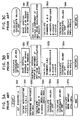
- Figs. 3A to 3C are flow-charts illustrating the algorithm. If it is assumed that the profile of each portion is depicted as shown in Fig. 2, in Step 310 of Fig. 3A, WINDOWs 1 and 2 shown in Fig. 2 are set by the area center-of-gravity calculating unit 22 and the lead-bend-amount calculating unit 25.
- Step 320 points a, b, c and d at which defining lines of the WINDOWs 1 and 2 and contour lines of the profile intersect each other are determined in Step 320.
- Step 330 mid-points between the respective pairs of points of intersection are determined and set as WG1 and WG2.
- Step 340 an angle ⁇ of inclination of the profile, i.e., an angle of bend, is determined from X-Y coordinate values of WG1 and WG2.
- Step 350 coordinates of a mid-point STP at one end of the profile are determined.
- the coordinates of STP are calculated as shown in Fig. 3B. Namely, in Step 351 of Fig.
- Step 352 a segment is extended from WG1 in parallel with the Y-axis. Then, in Step 352, the length of a segment A between the point WG1 and a point WG1VP is calculated. A segment B is determined from the segment A in Step 353. Then, the coordinates of STP are calculated in Step 354.
- Step 360 of Fig. 3A coordinate values of a mid-point SBP at the other end of the profile are determined in a similar manner in accordance with the flow-chart shown in Fig. 3C.
- Step 370 of Fig. 3A the difference between the X-axis components of the mid-points STP and SBP is calculated as the amount of bend.
- the non-defective/defective determining unit 24 allowable values of bend stored in advance in the external storage unit 26 are extracted, and a comparison is made between the same and the calculated amount of bend so as to determine the non-defective or defective state. Then, the horizontal transport mechanism section 5 is actuated by the sequencer 9, and the IC 2 whose non-defective or detective state has been determined is stored in the non-defective storage section 7 or the defective storage section 8. The inspection of the bend of IC leads has hitherto been effected automatically in the above-described manner.
- Figs. 4A to 4F are diagrams for explaining the problems in the conventional lead-bend measuring apparatus, in which Figs. 4A to 4D are graphs illustrating the distribution of illuminance at gradations, and Figs. 4E and 4F are diagrams illustrating the positions of sections in the leads.
- Figs. 4E and 4F are diagrams for explaining the problems in the conventional lead-bend measuring apparatus, in which Figs. 4A to 4D are graphs illustrating the distribution of illuminance at gradations, and Figs. 4E and 4F are diagrams illustrating the positions of sections in the leads.
- leads 39 are illuminated with light at sections 35a, 35b, 35c and 35d
- the distribution of illuminance differs for each of these sections, as shown in Figs. 9A to 9D.
- the sections 35a and 35b are imaged by one camera
- the sections 35c and 35d are imaged by another.
- an object of the present invention to provide a lead-bend measuring apparatus capable of effecting accurate measurement by making improvements on the binarization processing of a plurality of divided lead portions.
- a lead-bend measuring apparatus comprising: an illuminating means for projecting light onto leads projecting from a package of an integrated circuit device; an imaging means for imaging light reflected from and transmitted through the leads; a cutout means for fetching an image of the imaged light and dividing the image into a plurality of sections; a binarization processing means for processing gradations of the image with different binarization levels for each of the divided sections; a profile counter means for preparing profiles of various portions of the leads corresponding to the respective sections from binarized data subjected to processing by the binarization processing means; a calculating means for calculating a deviation of each of the prepared profiles from a reference profile and determining an amount of bend of each of the leads; and a means for determining a non-defective or defective state by making a comparison between the amount of bent calculated and allowable values.
- Fig. 5 is a block diagram of a lead-bend measuring apparatus in accordance with an embodiment of the present invention
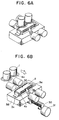
- Figs. 6A and 6B are enlarged perspective views of an inspection stage of the lead-bend measuring apparatus shown in Fig. 5
- Fig. 7 is a perspective view of a lower illuminating means for illuminating lead portions in the lead-bend measuring apparatus shown in Fig. 5.
- this lead-bend measuring apparatus is provided with binarization-level storage units 20b for storing the same number of binarization levels as the number of sections divided by an area cutout unit 16, as shown in Fig. 5.
- the lead-bend measuring apparatus of the present invention provided with the binarization-level storage units 20b is characterized in that clearer profiles of lead portions can be obtained as the binarization level selected for the dark and bright spots is changed in correspondence with the distribution of illuminance of light reflected from these sections.
- an IC 2 in Fig. 5 is gripped by a suction chuck of a horizontal transport mechanism section 5 which is controlled by a sequencer 9.
- the IC 2 is then moved horizontally and is transported from a feeding section 6 to an inspection stage 38.
- the IC 2 is placed on the inspection stage 38 with its rear surface facing upward, and is sucked with a vacuum so as to effect pre-alignment.
- the IC 2 is then fixed by means of a plurality of clamp claws 3a, 3b, 3c and 3d.
- the inspection stage 38 arranged in the state shown in Fig.
- the IC 2B is fed by a ball screw 30, and the IC 2 is positioned below a pair of annular incandescent lamps 4a, as shown in Fig. 6A. Then, the distal ends of the leads of the IC 2 and flat apex portions at their tops are irradiated by the annular incandescent lamps 4a, while the proximal ends of the leads are irradiated by a pair of optical fiber arrays 4b each comprised of optical fibers 4c and connected to an incandescent lamp-house 4d, as shown in Fig. 7.
- a pair of camera heads 1, a camera driver 10, and a camera controller 11 image the reflected images obtained thereby, and a fetch clock 12 and an 8-bit A/D converter 13 write the images to a frame memory 15 via I/O ports 14a with 256 gradations.
- a fetch clock 12 and an 8-bit A/D converter 13 write the images to a frame memory 15 via I/O ports 14a with 256 gradations.
- the area cutout unit 16 extracts a plurality of sections designated by area-designating-pointer storage units 19b, and divides the multivalued image data in the frame memory 15 into a plurality of sections.
- a binarization processing unit 17 fetches respective binarization levels corresponding to the sections from the binarization-level storage units 20b and effects binarization processing of the respective sections.
- the image data subjected to binarization processing is written to a binary image memory 18 via I/O ports 14d.
- an amount of bend of each lead is determined by a profile counter 21, an area-center-of-gravity calculating unit 22, and a lead-bend-amount calculating unit 25 by using the same algorithm as the one described for the prior art.
- the amount of bend of each lead thus calculated is compared with allowable values by a non-defective/defective determining unit 24 so as to determine the non-defective or defective state of the IC 2.
- Fig. 8 is a block diagram of the lead-bend measuring apparatus in accordance with another embodiment of the present invention.
- Fig. 9 is a perspective view of the inspection stage shown in Fig. 8 and an IC transport mechanism.
- a chute rail mechanism in which ICs are allowed to slide and drop by its own weight is adopted instead of the horizontal transport mechanism section which is used in the foregoing embodiment and in which each IC is gripped by a chuck and is moved. Namely, as shown in Fig.
- this IC transport mechanism comprises a chute rail 33a having a groove along which the package of the IC slides from the feeding section 6 onto the inspection stage 38; a positioning rail 33 having a vertically movable positioning stopper 34 at one end side thereof, the positioning rail 33 being secured on the inspection stage; and a pusher 33b for allowing the IC 2 discharged onto a placing table 33c from the positioning rail 33 to be dropped into a non-defective storage section 7 or a defective storage section 8 after completion of the inspection.
- the illuminating means of this lead-bend measuring apparatus is arranged such that a pair of rod-like parallel light sources 4e are arranged above the IC 2 and in parallel with the direction in which the leads are arrayed, and a reflecting mirror 32 for reflecting the light from the rod-like parallel light sources 4e is disposed substantially in the center of the IC 2 so as to illuminate the apex portions of the leads projecting from both sides of the IC 2 with this reflected light. Accordingly, the apex portions of the leads are imaged as transmitted images, and the distal ends as reflected images. In addition, the proximal ends of the leads are illuminated by the optical fiber arrays 4b in the same way as in the foregoing embodiment, and are imaged as reflected images.
- the IC 2 is first fed from the feeding section 6 to the chute rail 33a, the IC 2 slides along the chute rail 33a and drops onto the positioning rail 33.
- a sensor (not shown) is operated, and the stopper 34 is raised to position the IC 2.
- the IC 2 is then fixed by means of the clamp claws 3b and 3d.
- the camera heads 1, the camera driver 10, and the camera controller 11 pick up images, and the fetch clock 12 and the 8-bit A/D converter 13 write the images to the frame memory 15 with 256 gradations via the I/O ports 14a.
- the area cutout unit 16 cuts out the multivalued images into a plurality of sections designated by the area-designating-pointer storage units 19b.
- the binarization processing unit 17 then binarizes the cutout sections by using the binarization levels that are designated by the binarization-level storage units 20b on a one-to-one correspondence basis with respect to each section, and writes binarized image data to the binary image memory 18 through the I/O ports 14d.
- which portions of the images stored in the frame memory 15 are to be cut out is automatically transferred from an external storage unit 26 to the area-designating-pointer storage units 19b and is stored therein at the start of the apparatus.
- an operator of the apparatus is capable of newly preparing or revising these area-designating-pointer storage units 19b freely by operating a keyboard 27.
- the profile counter 21, the area-center-of-gravity calculating unit 22, and the lead-bend-amount calculating unit 25 calculate the amounts of bend of all the leads of the IC 2 on the basis of the binarized images which have been read through I/O ports 14e in accordance with the lead-bend calculating algorithm.
- the non-defective/defective determining unit 24 determines the non-defective or defective state by making a comparison with allowable values.
- the IC 2 for which the determination has been completed is discharged onto the placing table 33c from the positioning rail 33, and is transported to the non-defective storage section 7 or the defective storage section 7 by the pusher 33b.
- the apex portions of the leads are imaged as transmitted images, i.e., since images of the apex portions are stored in the binary image memory 18 as dark spots, the dark spots are converted to bright spots via an inverter 36 before they are fetched or loaded to the profile counter 21.
- the other portions of the leads i.e., the distal and proximal ends of the leads, are recorded in the binary image memory 18 as reflected images, i.e., bright spots, so that the image data thereof are processed as they are by the profile counter 21.
- a software switch 37 of a CPU 23 manages both an input line with the inverter 36 and a line without the same, and performs switching in such a manner as to effect inverted inputting with respect to the processing of the apex portions of the leads and non-inverted inputting with respect to the distal and proximal ends of the leads.
- the means for dividing the images of the leads into a plurality of sections and the means for setting binarization levels respectively corresponding to the divided sections and processing the sections with the corresponding binarization levels. Accordingly, there is an advantage in that even if the illuminance of the various portions of the leads is not uniform, it is possible to obtain clearer binarized images, thereby making it possible to effect measurements more accurately.
Landscapes
- Engineering & Computer Science (AREA)
- Physics & Mathematics (AREA)
- Health & Medical Sciences (AREA)
- General Physics & Mathematics (AREA)
- Microelectronics & Electronic Packaging (AREA)
- General Health & Medical Sciences (AREA)
- Immunology (AREA)
- Chemical & Material Sciences (AREA)
- Analytical Chemistry (AREA)
- Biochemistry (AREA)
- Manufacturing & Machinery (AREA)
- Operations Research (AREA)
- Life Sciences & Earth Sciences (AREA)
- Pathology (AREA)
- Computer Hardware Design (AREA)
- Computer Vision & Pattern Recognition (AREA)
- Electromagnetism (AREA)
- Toxicology (AREA)
- General Engineering & Computer Science (AREA)
- Length Measuring Devices By Optical Means (AREA)
- Testing Or Measuring Of Semiconductors Or The Like (AREA)
Applications Claiming Priority (2)
| Application Number | Priority Date | Filing Date | Title |
|---|---|---|---|
| JP29828/92 | 1992-02-18 | ||
| JP4029828A JPH06137839A (ja) | 1992-02-18 | 1992-02-18 | リード曲り測定装置 |
Publications (2)
| Publication Number | Publication Date |
|---|---|
| EP0560096A2 true EP0560096A2 (fr) | 1993-09-15 |
| EP0560096A3 EP0560096A3 (en) | 1993-11-03 |
Family
ID=12286891
Family Applications (1)
| Application Number | Title | Priority Date | Filing Date |
|---|---|---|---|
| EP19930102569 Withdrawn EP0560096A3 (en) | 1992-02-18 | 1993-02-18 | Apparatus for measuring bend amount of ic leads |
Country Status (3)
| Country | Link |
|---|---|
| US (1) | US5412477A (fr) |
| EP (1) | EP0560096A3 (fr) |
| JP (1) | JPH06137839A (fr) |
Cited By (5)
| Publication number | Priority date | Publication date | Assignee | Title |
|---|---|---|---|---|
| WO1994024700A1 (fr) * | 1993-04-16 | 1994-10-27 | Modular Vision Systems Inc. | Procede et systeme d'inspection de la qualite des fils situes sur un boitier plat quadruple |
| EP0678910A3 (fr) * | 1994-04-20 | 1996-04-17 | Siemens Ag | Système d'inspection de plaquettes semi-conductrices. |
| EP0678911A3 (fr) * | 1994-04-20 | 1996-04-17 | Siemens Ag | Système et appareil pour l'inspection des plaquettes semi-conductrices. |
| WO1999005702A1 (fr) * | 1997-07-23 | 1999-02-04 | Siemens Aktiengesellschaft | Controle et rectification d'agencements de contact defectueux dans des composants a semi-conducteurs integres |
| CN119984096A (zh) * | 2025-04-17 | 2025-05-13 | 洛阳理工学院 | 一种大型管件局部成形情况检测方法 |
Families Citing this family (2)
| Publication number | Priority date | Publication date | Assignee | Title |
|---|---|---|---|---|
| JP3298753B2 (ja) * | 1994-10-14 | 2002-07-08 | 株式会社新川 | ワイヤ曲がり検査装置 |
| US5877803A (en) * | 1997-04-07 | 1999-03-02 | Tritech Mircoelectronics International, Ltd. | 3-D image detector |
Family Cites Families (14)
| Publication number | Priority date | Publication date | Assignee | Title |
|---|---|---|---|---|
| JPS63181341A (ja) * | 1987-01-23 | 1988-07-26 | Toshiba Corp | リ−ド外観検査装置及びその検査方法 |
| JPS63265440A (ja) * | 1987-04-22 | 1988-11-01 | Mitsubishi Electric Corp | 半導体装置のリ−ド形状検査装置 |
| JPH01233349A (ja) * | 1988-03-14 | 1989-09-19 | Nec Corp | 半導体デバイスのリード曲り検出機 |
| JPH01265144A (ja) * | 1988-04-15 | 1989-10-23 | Sony Corp | 実装部品のリード変形チェック方法 |
| JPH02136707A (ja) * | 1988-11-16 | 1990-05-25 | Nec Corp | リード曲り検出機 |
| US4995157A (en) * | 1989-05-16 | 1991-02-26 | Reel-Tech Inc. | Component feeder system |
| JPH083405B2 (ja) * | 1989-06-30 | 1996-01-17 | 松下電器産業株式会社 | リード位置認識装置 |
| EP0711067A3 (fr) * | 1989-11-21 | 1996-07-10 | Toyo Ink Mfg Co | Procédé pour la formation de formes de densités pour la reproduction de gradations binaires |
| JP2946570B2 (ja) * | 1989-11-24 | 1999-09-06 | 日本電気株式会社 | コプラナリティ測定装置 |
| JPH03285341A (ja) * | 1990-04-02 | 1991-12-16 | M B K Maikurotetsuku:Kk | リードスキャナー |
| JP2870142B2 (ja) * | 1990-07-17 | 1999-03-10 | 日本電気株式会社 | コプラナリティ測定方法及びその装置 |
| JP2630034B2 (ja) * | 1990-07-24 | 1997-07-16 | 日本電気株式会社 | リード曲り測定装置 |
| US5168528A (en) * | 1990-08-20 | 1992-12-01 | Itt Corporation | Differential electronic imaging system |
| JPH04102346A (ja) * | 1990-08-22 | 1992-04-03 | Nec Corp | 半導体装置のリード曲り検査装置 |
-
1992
- 1992-02-18 JP JP4029828A patent/JPH06137839A/ja active Pending
-
1993
- 1993-02-17 US US08/018,864 patent/US5412477A/en not_active Expired - Fee Related
- 1993-02-18 EP EP19930102569 patent/EP0560096A3/en not_active Withdrawn
Cited By (5)
| Publication number | Priority date | Publication date | Assignee | Title |
|---|---|---|---|---|
| WO1994024700A1 (fr) * | 1993-04-16 | 1994-10-27 | Modular Vision Systems Inc. | Procede et systeme d'inspection de la qualite des fils situes sur un boitier plat quadruple |
| EP0678910A3 (fr) * | 1994-04-20 | 1996-04-17 | Siemens Ag | Système d'inspection de plaquettes semi-conductrices. |
| EP0678911A3 (fr) * | 1994-04-20 | 1996-04-17 | Siemens Ag | Système et appareil pour l'inspection des plaquettes semi-conductrices. |
| WO1999005702A1 (fr) * | 1997-07-23 | 1999-02-04 | Siemens Aktiengesellschaft | Controle et rectification d'agencements de contact defectueux dans des composants a semi-conducteurs integres |
| CN119984096A (zh) * | 2025-04-17 | 2025-05-13 | 洛阳理工学院 | 一种大型管件局部成形情况检测方法 |
Also Published As
| Publication number | Publication date |
|---|---|
| US5412477A (en) | 1995-05-02 |
| JPH06137839A (ja) | 1994-05-20 |
| EP0560096A3 (en) | 1993-11-03 |
Similar Documents
| Publication | Publication Date | Title |
|---|---|---|
| US4942618A (en) | Method and apparatus for determining the shape of wire or like article | |
| US5621530A (en) | Apparatus and method for verifying the coplanarity of a ball grid array | |
| JP4901903B2 (ja) | 三次元検査システム | |
| JP5421763B2 (ja) | 検査装置および検査方法 | |
| US5909285A (en) | Three dimensional inspection system | |
| JP2870142B2 (ja) | コプラナリティ測定方法及びその装置 | |
| EP1557876A1 (fr) | Lecteur de marque de sonde et procede de lecture d'une marque de sonde | |
| EP0222072A2 (fr) | Méthode et appareil pour placer un dispositif monté en surface | |
| JPH06103165B2 (ja) | 基板上の回路素子の高さ測定方法 | |
| JPH11351827A (ja) | 画像処理装置 | |
| JP3311135B2 (ja) | 検査範囲認識方法 | |
| JP3333615B2 (ja) | 半導体装置の寸法測定装置及び方法 | |
| US5412477A (en) | Apparatus for measuring bend amount of IC leads | |
| US5058177A (en) | Method for inspection of protruding features | |
| US20030001117A1 (en) | Dimensional measurement apparatus for object features | |
| JP2000131037A (ja) | 物体形状検査装置 | |
| KR20000054979A (ko) | 집적회로 패키지의 리드핀 납땜 검사방법 및 검사장치 | |
| JP3219094B2 (ja) | チップサイズ検出方法およびチップピッチ検出方法およびチップ配列データ自動作成方法ならびにそれを用いた半導体基板の検査方法および装置 | |
| JPH0429007A (ja) | 光学検査装置 | |
| JP2630034B2 (ja) | リード曲り測定装置 | |
| JPH07119705B2 (ja) | 電子部品の検査装置 | |
| JPH11211420A (ja) | 光学式寸法測定方法および装置 | |
| JP2946570B2 (ja) | コプラナリティ測定装置 | |
| JP2003065754A (ja) | 半導体装置実装体の平坦度検査方法及び装置 | |
| JP3621222B2 (ja) | 半導体基板のパターン配列認識方法 |
Legal Events
| Date | Code | Title | Description |
|---|---|---|---|
| PUAI | Public reference made under article 153(3) epc to a published international application that has entered the european phase |
Free format text: ORIGINAL CODE: 0009012 |
|
| AK | Designated contracting states |
Kind code of ref document: A2 Designated state(s): DE FR GB |
|
| PUAL | Search report despatched |
Free format text: ORIGINAL CODE: 0009013 |
|
| AK | Designated contracting states |
Kind code of ref document: A3 Designated state(s): DE FR GB |
|
| 17P | Request for examination filed |
Effective date: 19930927 |
|
| 17Q | First examination report despatched |
Effective date: 19950620 |
|
| STAA | Information on the status of an ep patent application or granted ep patent |
Free format text: STATUS: THE APPLICATION IS DEEMED TO BE WITHDRAWN |
|
| 18D | Application deemed to be withdrawn |
Effective date: 19960103 |