EP0563640A1 - Dispositif de guidage pour une bande magnétique - Google Patents
Dispositif de guidage pour une bande magnétique Download PDFInfo
- Publication number
- EP0563640A1 EP0563640A1 EP93103898A EP93103898A EP0563640A1 EP 0563640 A1 EP0563640 A1 EP 0563640A1 EP 93103898 A EP93103898 A EP 93103898A EP 93103898 A EP93103898 A EP 93103898A EP 0563640 A1 EP0563640 A1 EP 0563640A1
- Authority
- EP
- European Patent Office
- Prior art keywords
- magnetic tape
- circuit
- magnetic
- guide
- data
- Prior art date
- Legal status (The legal status is an assumption and is not a legal conclusion. Google has not performed a legal analysis and makes no representation as to the accuracy of the status listed.)
- Granted
Links
Images








Classifications
-
- G—PHYSICS
- G11—INFORMATION STORAGE
- G11B—INFORMATION STORAGE BASED ON RELATIVE MOVEMENT BETWEEN RECORD CARRIER AND TRANSDUCER
- G11B15/00—Driving, starting or stopping record carriers of filamentary or web form; Driving both such record carriers and heads; Guiding such record carriers or containers therefor; Control thereof; Control of operating function
- G11B15/60—Guiding record carrier
- G11B15/61—Guiding record carrier on drum, e.g. drum containing rotating heads
-
- G—PHYSICS
- G11—INFORMATION STORAGE
- G11B—INFORMATION STORAGE BASED ON RELATIVE MOVEMENT BETWEEN RECORD CARRIER AND TRANSDUCER
- G11B15/00—Driving, starting or stopping record carriers of filamentary or web form; Driving both such record carriers and heads; Guiding such record carriers or containers therefor; Control thereof; Control of operating function
- G11B15/60—Guiding record carrier
- G11B15/66—Threading; Loading; Automatic self-loading
- G11B15/665—Threading; Loading; Automatic self-loading by extracting loop of record carrier from container
Definitions
- This invention relates to a magnetic tape guide apparatus for guiding a magnetic tape.
- a magnetic tape guide apparatus is incorporated in various magnetic recording and/or reproducing apparatus in which a magnetic tape is employed as a magnetic record medium.
- An exemplary one of such magnetic recording and/or apparatus is a video tape recorder.
- An exemplary one of conventional magnetic tape guide apparatus for use with a video tape recorder is shown in Fig. 22.
- the magnetic tape guide apparatus shown includes a magnetic head drum 3 including a pair of upper and lower magnetic tape guide drums 1 and 2 having an equal diameter are disposed on a common axis.
- a magnetic tape 4 is guided obliquely along a circumferential face of the magnetic head drum 3 while recording onto or reproduction from the magnetic tape 4 is performed by a rotary magnetic head 5 located between the drums 1 and 2.
- the magnetic tape guide apparatus further includes a fixed guide pin 6 disposed intermediately of the path of the magnetic tape 4 for guiding the magnetic tape 4.
- One of the guide drums 1 and 2 of the magnetic head drum 3, for example, the drum 1, is formed as a rotary drum while the other drum 2 is formed as a fixed drum.
- magnetic thin metal film magnetic tapes wherein a magnetic layer is formed by vapor deposition, sputtering or the like of magnetic metal having a high coercive force such as Co-Ni, Co-Cr or Co-O type metal.
- the form of a signal is changing from an analog signal into a digital signal, and designing of a record medium in accordance with the form of a signal together with an increase of the recording density is required.
- in-plane magnetic recording method wherein a magnetic record medium having a magnetization-easy axis in a plane thereof is employed most popularly.
- the magnetization directions of magnetization sections on the magnetic record medium are arranged such that, as the recording density increases, adjacent magnetization sections repel each other by an increasing repulsive force. Accordingly, there naturally is a limitation in increase of the recording density, and it is difficult to achieve recording of a required high density.
- the demagnetizing action is very little comparing with the in-plane magnetic recording method, and it is possible to remarkably increase the recording density.
- a magnetic thin metal film magnetic tape of the Co-Ni, Co-Cr or Co-O type which has a superior magnetic characteristic as a perpendicular magnetic record medium or a magnetic film wherein a protective film of carbon or ZnO2 for assuring a high durability and corrosion resistance is provided on a magnetic thin metal film is used.
- the countermeasure for the problem of sticking of a magnetic tape to a guide drum or a guide pin, particularly to a fixed guide drum or a fixed guide pin which guides a magnetic tape in a slidably contacting condition is normally provided by selection of a metal material constituting the guide drum or the guide pin (guide member), roughening of the surface of the guide member and so forth.
- the inventors of the present invention have made various investigations for a cause of sticking of a magnetic tape to a magnetic tape guide face of a guide drum or a guide pin and discovered the fact that such sticking, which brings up an increase of the coefficient of friction, arises from molecules of water attracted to the contacting faces of the magnetic tape and the guide member, based on establishment of a method of measurement of a film thickness of a layer of such attracted molecules of water. Then, based on the discovery, the inventors have invented a magnetic tape guide apparatus of the present invention which is superior in transport performance of a magnetic tape.
- the height ⁇ of crests of the guide face 11, that is, the maximum height Rmax of the surface was 1 ⁇ m
- the mark ⁇ in Fig. 24 represents data obtained when the environmental temperature was 25 °C while the marks ⁇ and ⁇ represent data obtained when the environmental temperature was 40 °C and 50 °C, respectively.
- a drum to be measured or a pin D is disposed in such a manner as shown in Fig. 25, and a magnetic tape 4 is guided over the angle of ⁇ around a circumferential face of the drum or the pin D.
- a weight W is coupled to an end of a tape 4 so that tension T1 is applied to the tape 4 from the weight W while a measurement of tension T2 is performed at the other end of the tape 4 by means of a force detector M.
- T2/T1 e ⁇ (1)
- ⁇ (1/ ⁇ ) 1n(T2/T1) (2)
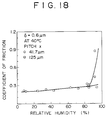
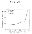
- the coefficient ⁇ of friction relies only upon the film thickness of an attracted water molecule layer and increases suddenly at a particular film thickness.
- the friction between the magnetic tape 4 and the guide face 11, for example, of the fixed drum relies not only upon shearing at a coupling portion provided by direct contact of the two metals with each other but also upon destruction of the attracted water molecules around the coupling portion, and based on this fact, the present invention provides a structure which effectively prevents, even in a high humidity condition, production of an attracted water layer having a film thickness which brings about such a disadvantage.
- a magnetic tape guide face 11 of a guide member 7 for a magnetic tape that is, a guide drum or a guide pin
- the height ⁇ of crests that is, a maximum height Rmax
- the pitch x of the crests satisfies the following equation 3: 0.050 mm ⁇ x ⁇ (329 ⁇ ) 1/4 mm (3)
- the radius of the guide member 7 for a magnetic tape is set to 0.7 mm to 12 mm.
- the present invention exhibits a significant advantage particularly when it is applied to a digital video tape recorder wherein the error rate is suppressed to the order of 10-5.
- a magnetic tape guide apparatus is useful when it is applied to a digital tape recorder wherein a color video signal is digitized and recorded onto a magnetic tape and particularly the error rate is reduced lower than the order of 10 ⁇ 5.
- the magnetic recording and reproducing apparatus that is, the digital video tape recorder, will be described in accordance with the following order.
- component type digital video tape recorders of the D1 format and composite type digital video tape recorders of the D2 format for broadcasting stations have been put into practical use.
- the former D1 format digital video tape recorders convert a brightness signal and first and second color difference signals by analog to digital conversion with the sampling frequencies of 13.5 MHz and 6.75 MHz, respectively, and then perform predetermined processing to record the signals onto a magnetic tape. Since the sampling frequencies of the components make the ratio of 4:2:2, the system is called 4:2:2 system.
- the latter D2 format digital video tape recorders effect sampling of a composite color video signal with a signal of a frequency which is equal to four times the frequency of a color subcarrier signal to effect analog to digital conversion of the composite color video signal and then performs predetermined signal processing, whereafter it records the thus processed signal onto a magnetic tape.
- the digital video tape recorders mentioned above are designed on the assumption that they are both used for broadcasting stations, they give priority to the picture quality and are constructed so that a digital color video signal wherein one sample is converted into, for example, 8 bits by analog to digital conversion is recorded substantially without compressing it.
- a signal of the shortest wavelength of 0.5 ⁇ m is recorded within the track width of, for example, 5 ⁇ m so that the recording density of 4 x 105 bit/mm2 or 8 x 105 bit/mm2 or more is realized, and by additionally employing a method which compresses recording information in such a form that it involves little reproduction distortion, the present invention is applied to a digital video tape recorder which can record and reproduce for a long time even when a narrow magnetic tape having a tape width W T of 8 mm or less is used.
- Fig. 2 there is shown general construction of an entire recording system of the digital video tape recorder.
- the recording system shown has input terminals 1Y, 1U and 1V to which a digital brightness signal Y and digital color difference signals U and V formed from three primary color signals R, G and B, for example, from a color video camera are supplied, respectively.
- the clock rates of the input signals are equal to the frequencies of component signals of the D1 format.
- the sampling frequencies of the digital brightness signal Y and the digital color difference signals U and V are 13.5 MHz and 6.75 MHz, respectively, and the number of bits per one sample of the signals is 8 bits.
- the amount of data of signals supplied to the input terminals 1Y, 1U and 1V is about 216 Mbps (megabits/second).
- the amount of data is compressed to about 167 Mbps by an effective information extraction circuit 102 which removes data for a blanking time from the input signals but extracts only information in an effective region.
- the brightness signal Y is supplied to a frequency conversion circuit 103, by which the sampling frequency is reduced from 13.5 MHz to three fourths of the same.
- a thinning out filter is used as the frequency conversion circuit 103 so as to prevent loopback distortion.
- An output signal of the frequency conversion circuit 103 is supplied to a blocking circuit 105, by which the order of the brightness data is changed into the order of blocks.
- the blocking circuit 105 is provided for a block coding circuit 108 provided at a succeeding stage.
- Fig. 3 illustrates the structure of a block which is a unit of coding.
- the block shown is a three-dimensional block, and as shown in Fig. 3, a large number of unit blocks of 4 lines ⁇ 4 picture elements ⁇ 2 frames are formed, for example, by dividing a screen which spans two frames. It is to be noted that, in Fig. 3, each solid line indicates a line of an odd-numbered field while each broken line indicates a line of an even-numbered field.
- the two color difference signals U and V are supplied to a sub-sampling and sub-line circuit 104, by which the sampling frequencies of them are reduced from 6.75 MHz to one half of the same and then the two digital color difference signals are selected alternately line by line so that they are composed into data of one channel. Consequently, a line sequential digital color difference signal is obtained from the sub-sampling and sub-line circuit 104.
- Fig. 4 The construction of picture elements of the signal obtained by sub-sampling and sub-lining by the sub-sampling and sub-line circuit 104 is illustrated in Fig. 4.
- the mark ⁇ indicates a sub-sampled picture element of the first color difference signal U;
- the mark ⁇ indicates a sub-sampled picture element of the second color difference signal; and
- the mark ⁇ indicates the position of a picture element thinned out by sub-sampling.
- the line sequential output signal of the sub-sampling and sub-line circuit 104 is supplied to a blocking circuit 106.
- the color difference data of the order of operation of the television signal is converted into data of the order of blocks, similarly as in the blocking circuit 105.
- the blocking circuit 106 converts the color difference data into data of the block structure of 4 lines ⁇ 4 picture elements ⁇ 2 frames, similarly to the blocking circuit 105.
- Output signals of the blocking circuits 105 and 106 are supplied to a composing circuit 107.
- the composing circuit 107 the brightness signal and the color difference signal after conversion into the signals of the order of blocks are converted into data of one channel, and an output signal of the composing circuit 107 is supplied to a block coding circuit 108.
- a block coding circuit 108 a coding circuit (called ADRC (Adaptive Dynamic Range Coding) circuit) adaptive to a dynamic range for each block, a DCT (Discrete Cosine Transform) circuit and so forth can be applied.
- An output signal of the block coding circuit 108 is supplied to a framing circuit 109, in which it is converted into data of a frame structure. In the framing circuit 109, crossing-over between clocks of the picture element system and clocks of the recording system is performed.
- an output signal of the framing circuit 109 is supplied to a parity generation circuit 110 for an error correction code, in which a parity of an error correction code is generated.
- An output signal of the parity generating circuit 110 is supplied to a channel encoder 111, in which such channel coding as to decrease a low frequency portion of recording data is performed.
- An output signal of the channel encoder 111 is supplied to a pair of magnetic heads 113A and 113B by way of a pair of recording amplifiers 112A and 112B and a pair of respective rotary transformers not shown so that it is recorded onto a magnetic tape not shown. It is to be noted that an audio signal is compressed and coded separately from the video signal and supplied to the channel encoder 111.
- the amount of input data of 216 Mbps is reduced to about 167 Mbps by extraction only of data in the effective scanning period and is further reduced to 84 Mbps by frequency conversion and sub-sampling/sub-lining.
- the data is then compressed to about 25 Mbps by compression coding by the block coding circuit 108, and the final amount of data is 31.56 Mbps due to addition of additional information of a parity, an audio signal and so forth after then.
- reproduction data from the magnetic heads 113A and 113B are first supplied to a channel decoder 115 by way of the rotary transformers and a pair of reproduction amplifiers 114A and 114B, respectively.
- the channel decoder 115 decodes the channel-coded data, and an output signal of the channel decoder 115 is supplied to a TBC circuit (time base correction circuit) 116.
- TBC circuit 116 time base variation components of the reproduction signal are removed.
- Reproduction data from the TBC circuit 116 is supplied to an ECC circuit 117, in which error correction and error modification are performed using an error correction code.
- An output signal of the ECC circuit 117 is supplied to a deframing circuit 118.
- deframing circuit 118 By the deframing circuit 118, components of the block coded data are separated from one another and crossing-over from clocks of the recording system to clocks of the picture element system is performed.
- the data separated by the deframing circuit 118 are supplied to a block decoding circuit 119, by which the data are decoded into restoration data corresponding to original data for each block unit.
- the decoded data is supplied to a distribution circuit 120.
- the decoded data is separated into a brightness signal and a color difference signal by the distribution circuit 120.
- the brightness signal and the color difference signal are supplied to a pair of deblocking circuits 121 and 122, respectively.
- the deblocking circuits 121 and 122 convert the decoded data of the order of blocks into data of the raster scanning order, reversely to the blocking circuits 105 and 106 on the recording side.
- the decoded block signal from the deblocking circuit 121 is supplied to an interpolation filter 123.
- the digital brightness signal Y from the interpolation filter 123 is extracted to an output terminal 126Y.
- the digital color difference signal from the deblocking circuit 121 is supplied to another distribution circuit 124, in which the line sequential digital color difference signal U and V is separated into digital color difference signals U and V.
- the color difference signals U and V from the distribution circuit 124 are supplied to another interpolation circuit 125, in which they are interpolated.
- the interpolation circuit 125 interpolates the lines and the picture elements, which have been thinned out, using the restored picture element data.
- a pair of digital color difference signals U and V of the sampling rate of 2fs are obtained from the interpolation circuit 125 and extracted to output terminals 126U and 126V, respectively.
- An ADRC encoder is employed as the block coding circuit 108 in Fig. 2.
- the ADRC encoder detects a maximum value MAX and a minimum value MIN of a plurality of picture element data included in each block, detects a dynamic range DR of the block from the maximum value MAX and the minimum value MIN, effects coding of the data in accordance with the dynamic range DR, and requantizes the coded data with a number of bits smaller than the number of bits of the original picture element data.
- the block coding circuit 108 may alternatively be constructed such that picture element data of each block are first processed by DCT processing and then coefficient data obtained by the DCT processing are quantized, whereafter the quantized data are coded by run-length Huffman coding to compress and code them.
- a digital video signal or a digital color difference signal wherein, for example, one sample is quantized into 8 bits is inputted to an input terminal 27 from the composing circuit 107 of Fig. 2.
- the blocked data from the input terminal 27 is supplied to a maximum/minimum value detection circuit 29 and a delay circuit 30.
- the maximum/minimum value detection circuit 29 detects a minimum value MIN and a maximum value MAX for each block.
- the delay circuit 30 delays the input data by a time required for a maximum value and a minimum value to be detected.
- Picture element data from the delay circuit 30 are supplied to a pair of comparison circuits 31 and 32.
- the maximum value MAX from the maximum/minimum value detection circuit 29 is supplied to a subtraction circuit 33 while the minimum value MIN is supplied to an addition circuit 34.
- the bit shift circuit 35 is constructed so as to shift the dynamic range DR by 4 bits in order to effect a dividing operation of 1/16.
- a threshold value of MAX - ⁇ is obtained from the subtraction circuit 33 while another threshold value of MIN + ⁇ is obtained from the addition circuit 34.
- the threshold values from the subtraction circuit 33 and the addition circuit 34 are supplied to a pair of comparison circuits 31 and 32, respectively. It is to be noted that the value ⁇ which defines the threshold values is not limited to a quantization step width but may be a fixed value corresponding to a noise level.
- An output signal of the comparison circuit 31 is supplied to an AND gate 36 while an output signal of the other comparison circuit 32 is supplied to another AND gate 37.
- the input data from delay circuit 30 are supplied to the AND gates 36 and 37.
- the output signal of the comparison circuit 31 presents a high level when the input data thereto is higher than the threshold value thereto, and accordingly, picture element data of the input data included in a maximum level range of MAX to MAX - ⁇ are extracted to the output terminal of the AND gate 36.
- the output signal of the other comparison circuit 32 presents a high level when the input data thereto is lower than the threshold value thereto, and accordingly, picture element data of the input data included in a minimum level range of MIN to MIN + ⁇ are extracted to the output terminal of the AND gate 37.
- An output signal of the AND gate 36 is supplied to an averaging circuit 38 while an output signal of the AND gate 37 is supplied to another averaging circuit 39.
- Each of the averaging circuit 38 and 39 calculates an average value for each block, and a reset signal having the period of one block is supplied from a terminal 40 to the averaging circuits 38 and 39.
- An average value MAX' of picture element data belonging to the maximum level range of MAX to MAX - ⁇ is obtained from the averaging circuit 38 while another average value MIN' of picture element data belonging to the minimum level range of MIN to MIN + ⁇ is obtained from the other averaging circuit 39.
- the average value MIN' is subtracted from the average value MAX' by a subtraction circuit 41 so that a dynamic range DR' is obtained from the subtraction circuit 41.
- the average value MIN' is supplied to another subtraction circuit 42, in which the average value MIN' is subtracted from the input data inputted thereto by way of a delay circuit 43 so that data PDI after removal of minimum values therefrom are formed.
- the data PDI and the modified dynamic range DR' are supplied to a quantization circuit 44.
- the ADRC is variable length ADRC wherein the number n of bits allocated to quantization is one of 0 bit (no code signal is to be transmitted), 1 bit, 2 bits, 3 bits and 4 bits, and edge matching quantization is performed.
- the allocated bit number n is determined for each block by a bit number determination circuit 45, and the data of the bit number n is supplied to the quantization circuit 44.
- the bit number n is made small for a block having a small dynamic range DR', but the bit number n is made large for another block having a large dynamic range DR' so that efficient coding may be performed.
- T1 to T4 T1 ⁇ T2 ⁇ T3 ⁇ T4
- variable length ADRC the amount of information to be generated can be controlled (so-called buffering) by varying the threshold values T1 to T4. Accordingly, the variable length ADRC can be applied to such a transmission line as of a digital audio video tape recorder of the present embodiment for which it is required that the amount of information to be generated for one field or one frame be set to a predetermined value.
- a buffering circuit 46 for determining the threshold values T1 to T4 to make the amount of information to be generated a predetermined value a plurality of, for example, 32, sets of threshold values (T1, T2, T3, T4) are prepared.
- i 1, 1, 2, ..., 31.
- the threshold values T1 to T4 from the buffering circuit 46 are supplied to a comparison circuit 47 while the dynamic range DR' is supplied to the comparison circuit 47 by way of a delay circuit 48.
- the delay circuit 48 delays the dynamic range DR' by a time required for a set of threshold values to be determined by the buffering circuit 46.
- the comparison circuit 47 the dynamic range DR' of the block and the threshold values are successively compared with each other, and a result of the comparison is supplied to the bit number determination circuit 45, in which the allocated bit number n of the block is determined.
- the quantization circuit 44 the data PDI after removal of minimum values therefrom, which are received by way of a delay circuit 49, are converted into a code signal DT by edge matching quantization using the dynamic range DR' and the allocated bit number n.
- the quantization circuit 44 may be constituted, for example, from a ROM.
- the modified dynamic ranges DR' and the modified average value MIN' are outputted from the block coding circuit 108 of Fig. 6 by way of a pair of delay circuits 48 and 50, respectively, and further, the code signal DT and the parameter Pi indicative of the set of threshold values are outputted from the block coding circuit 108.
- the present block coding circuit 108 since a signal quantized once by non-edge matching quantization is newly quantized by edge matching quantization based on dynamic range information, the image deterioration involved in dubbing is reduced.
- the channel encoder 111 includes a plurality of M sequence scramble circuits 51 in the form of adaptive scramble circuits to which the output of the parity generation circuit 110 shown in Fig. 2 is supplied and which are constructed so that an M sequence with which an output which presents least high frequency components and dc components for the input signal is obtained may be selected.
- a precoder 52 for a partial response class 4 detection system is connected to each adaptive scramble circuit 51 and performs calculation processing of 1/(1-D2) (D denotes a delay time of a unit delay circuit).
- the output of the precoder 52 is recorded by the magnetic heads 113A and 113B by way of the recording amplifiers 112A and 112B and reproduced by the magnetic heads 113A and 113B, respectively, and the reproduction outputs are amplified by the reproduction amplifiers 114A and 114B.
- the channel decoder 115 includes a reproduction side calculation circuit 53 of the partial response class 4, which performs calculation of 1 + D for the outputs of the reproduction amplifiers 114A and 114B.
- a so-called bitervi decoding circuit 54 is connected to the calculation circuit 53 and effects calculation for the output of the calculation circuit 53 using correlation, probability or the like of data to achieve decoding of data which is tough against noise.
- the output of the bitervi decoding circuit 54 is supplied to a descramble circuit 55, in which the data, which have been rearranged by the scrambling processing by the recording circuit, are returned into data of the original sequence to restore the original data.
- the bitervi decoding circuit 54 employed in the present embodiment, a gain of 3 dB when converted into a reproduction C/N value is obtained, which is improved comparing with that by decoding for each bit.
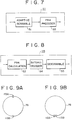
- the magnetic heads 113A and 113B described above are either mounted at an angular distance of 180° on a drum 76 as shown, for example, in Fig. 9A or mounted on the drum 76 in the form of, for example, an integrated structure as shown in Fig. 9B.
- a magnetic tape (not shown) is wrapped obliquely over a wrapping angular range a little larger or a little smaller than 180° on a circumferential face of the drum 76.
- the magnetic heads 113A and 113B contact almost alternately with the magnetic tape, but in the head arrangement shown in Fig. 9B, the magnetic heads 113A and 113B scan the magnetic tape simultaneously with each other.
- the magnetic heads 113A and 113B are constructed such that the extending angles of gaps thereof (called azimuth angles) are different from each other.
- azimuth angles the azimuth angles of ⁇ 20° are set to the magnetic heads 113A and 113B, and due to the difference between the azimuth angles, a signal is recorded onto a magnetic tape such that, as seen from a recording pattern in Fig. 11, on adjacent tracks TA and TB, it is inclined in the opposite directions to each other with angles corresponding to the azimuth angles. Accordingly, upon reproduction, the amount of crosstalk between adjacent tracks can be reduced by an azimuth loss.
- Figs. 12 and 13 show more detailed construction when the magnetic heads 113A and 113B are formed into an integrated structure (so-called double azimuth head).
- the magnetic heads 113A and 113B of the integrated structure are mounted on an upper guide drum 76 which is rotated at a high speed of, for example, 150 rps (NTSC system) while a lower guide drum 77 is fixed. Accordingly, data of one field are divided into and recorded onto 5 tracks on a magnetic head 78. The length of tracks can be reduced by the present segment system.
- the wrapping angle ⁇ of the magnetic tape 78 is, for example, 166°, and the drum diameter ⁇ is 16.5 mm.
- vibrations of the magnetic tape 78 are caused by eccentricity or the like of a rotating portion of the upper drum 76, and such vibrations cause an error in linearity of a track.
- the magnetic tape 78 is held downwardly, and as indicated by an arrow mark u in Fig. 14B, the magnetic tape 78 is drawn upwardly. Consequently, the magnetic tape 78 is vibrated, resulting in linearity of a track.
- the amount of such error in linearity can be decreased by simultaneous recording with the double azimuth head.
- the double azimuth head is advantageous in that, since the distance between the heads is small, pairing adjustment can be performed with a higher degree of accuracy. Recording and reproduction of a narrow track can be performed by such tape and head system.
- the present invention can be applied to a magnetic tape guide apparatus for the magnetic heads shown, for example, in Figs. 9, 12 and 13 of the digital video tape recorder described above.
- the drums 76 for guiding the magnetic tape 78 is worked to roughen the surface thereof, that is, the magnetic tape guide face 11 thereof as shown in Fig. 1 by forming fine grooves along a circumferential direction on a circumferential face of a tubular metal member made of, for example, aluminum, an aluminum alloy or stainless steel by means of an NC (numerically controlled) machine tool.
- the height ⁇ of crests of the roughened face is selected to range from 0.2 ⁇ m to 3.0 ⁇ m.
- the reason why the height ⁇ is selected to be equal to or higher than 0.2 ⁇ m is that, where the height ⁇ is lower than 0.2 ⁇ m, if the humidity becomes high, a sudden rise of frictional resistance takes place almost irrespective of the pitch x which is selected when the humidity is comparatively low.
- the height ⁇ exceeds 0.3 ⁇ m, then this may possibly have a bad influence on the roundness of the drum.
- the width W T of a magnetic tape for use with the digital video tape recorders is selected to be, for example, 6 mm, and in this connection, the radius of the guide drums 76 and 77 is set to be equal to or less than 12 mm taking a tracking error into consideration.
- ⁇ > 3.0 ⁇ m a significant influence is had on the roundness, and there is the possibility that stabilized transport of a magnetic tape may be obstructed.
- a pair of drums made of an aluminum ally were prepared wherein the height ⁇ of crests on the surfaces of the drums, that is, the surface maximum roughness, is 1 ⁇ m and the pitch of the crests, that is, the working pitch x, is 47 ⁇ m and 75 ⁇ m, and a transport test was conducted slidably contacting a magnetic thin metal film magnetic tape on the market with the drums.
- Table 1 Pitch x 47 ⁇ m 75 ⁇ m Coefficient of Friction ⁇ 40°C 11%RH 0.21 0.21 40°C 85%RH 0.32 0.29 40°C 95%RH 0.73 0.43
- the difference in coefficient of friction originating in the pitch x little takes place within the range of 85 %RH (relative humidity) or so at 40 °C, and damage to the magnetic tape side does not present a difference between the pitches and the magnetic tape suffers from little damage.
- N 2T sin(1/2r) (6)
- ⁇ max ⁇ .
- W T 6 mm.
- the present invention since an increase of friction in a high humidity condition can be suppressed effectively, the present invention exhibits considerable contribution to reduction of the error rate and can be suitably applied particularly to a digital video tape recorder which is aimed to the error rate of 10 ⁇ 5 order.
Landscapes
- Television Signal Processing For Recording (AREA)
- Signal Processing For Digital Recording And Reproducing (AREA)
- Magnetic Record Carriers (AREA)
- Conveying Record Carriers (AREA)
Applications Claiming Priority (2)
| Application Number | Priority Date | Filing Date | Title |
|---|---|---|---|
| JP55668/92 | 1992-03-13 | ||
| JP5566892 | 1992-03-13 |
Publications (2)
| Publication Number | Publication Date |
|---|---|
| EP0563640A1 true EP0563640A1 (fr) | 1993-10-06 |
| EP0563640B1 EP0563640B1 (fr) | 1997-09-03 |
Family
ID=13005245
Family Applications (1)
| Application Number | Title | Priority Date | Filing Date |
|---|---|---|---|
| EP93103898A Expired - Lifetime EP0563640B1 (fr) | 1992-03-13 | 1993-03-10 | Dispositif de guidage pour une bande magnétique |
Country Status (4)
| Country | Link |
|---|---|
| US (1) | US5914840A (fr) |
| EP (1) | EP0563640B1 (fr) |
| KR (1) | KR100258042B1 (fr) |
| DE (1) | DE69313493T2 (fr) |
Families Citing this family (5)
| Publication number | Priority date | Publication date | Assignee | Title |
|---|---|---|---|---|
| US7106794B2 (en) * | 2000-08-11 | 2006-09-12 | Broadcom Corporation | System and method for Huffman shaping in a data communication system |
| JP2002313057A (ja) * | 2001-04-18 | 2002-10-25 | Fuji Photo Film Co Ltd | 磁気テープカセット |
| US20030089819A1 (en) * | 2001-11-14 | 2003-05-15 | Bloomquist Darrel R. | Irregular surfaced tape guide |
| JP2003331557A (ja) * | 2002-05-10 | 2003-11-21 | Fuji Photo Film Co Ltd | 記録テープカセット |
| CA2514078C (fr) * | 2002-12-31 | 2012-07-10 | Ossur Hf | Pansement de plaie |
Citations (6)
| Publication number | Priority date | Publication date | Assignee | Title |
|---|---|---|---|---|
| DE2830615A1 (de) * | 1978-07-12 | 1980-01-31 | Basf Ag | Fuehrungseinrichtung fuer einen duennen bandfoermigen aufzeichnungstraeger, insbesondere fuer ein magnetband |
| DE2840069B2 (de) * | 1977-09-14 | 1981-05-27 | Yozaburo Tokyo Umehara | Bandführungseinrichtung für ein Aufzeichnungs- und/oder Wiedergabegerät, sowie Herstellverfahren dafür |
| EP0050737A1 (fr) * | 1980-10-27 | 1982-05-05 | BASF Aktiengesellschaft | Dispositif de renvoi pour un support d'enregistrement, en particulier pour une bande magnétique |
| EP0057409A2 (fr) * | 1981-01-29 | 1982-08-11 | Johann Bischl | Elément de guidage |
| EP0187319A1 (fr) * | 1984-12-24 | 1986-07-16 | BASF Aktiengesellschaft | Mécanisme de guidage de bande pour dispositifs d'entraînement de bande, particulièrement dispositifs de bande magnétique, et cassettes à bande avec ce mécanisme |
| US4669019A (en) * | 1980-08-30 | 1987-05-26 | Sony Corporation | Magnetic head drum assembly |
Family Cites Families (8)
| Publication number | Priority date | Publication date | Assignee | Title |
|---|---|---|---|---|
| US4437222A (en) * | 1977-09-14 | 1984-03-20 | Yozaburo Umehara | Method of manufacturing tape guides for recording and/or reproducing apparatus |
| JPS5552552A (en) * | 1978-10-09 | 1980-04-17 | Shiro Okamura | Reproducing device |
| JPS56115788U (fr) * | 1980-02-06 | 1981-09-04 | ||
| JPS578948A (en) * | 1980-06-18 | 1982-01-18 | Hitachi Ltd | Magnetic tape guide device |
| JPS5852679U (ja) * | 1981-10-06 | 1983-04-09 | ティーディーケイ株式会社 | 磁気テ−プカ−トリツジ用テ−プガイド |
| JPS6289289A (ja) * | 1985-10-15 | 1987-04-23 | Masamitsu Tanaka | 軽量テ−プ案内筒及びその製造方法 |
| US4745508A (en) * | 1985-11-13 | 1988-05-17 | Minnesota Mining And Manufacturing Company | Plastic supply tape guide for videocassette |
| JPS62256254A (ja) * | 1986-04-28 | 1987-11-07 | Hitachi Ltd | 回転ヘツド装置 |
-
1993
- 1993-02-24 KR KR1019930002539A patent/KR100258042B1/ko not_active Expired - Fee Related
- 1993-03-10 DE DE69313493T patent/DE69313493T2/de not_active Expired - Lifetime
- 1993-03-10 EP EP93103898A patent/EP0563640B1/fr not_active Expired - Lifetime
- 1993-03-11 US US08/029,549 patent/US5914840A/en not_active Expired - Lifetime
Patent Citations (6)
| Publication number | Priority date | Publication date | Assignee | Title |
|---|---|---|---|---|
| DE2840069B2 (de) * | 1977-09-14 | 1981-05-27 | Yozaburo Tokyo Umehara | Bandführungseinrichtung für ein Aufzeichnungs- und/oder Wiedergabegerät, sowie Herstellverfahren dafür |
| DE2830615A1 (de) * | 1978-07-12 | 1980-01-31 | Basf Ag | Fuehrungseinrichtung fuer einen duennen bandfoermigen aufzeichnungstraeger, insbesondere fuer ein magnetband |
| US4669019A (en) * | 1980-08-30 | 1987-05-26 | Sony Corporation | Magnetic head drum assembly |
| EP0050737A1 (fr) * | 1980-10-27 | 1982-05-05 | BASF Aktiengesellschaft | Dispositif de renvoi pour un support d'enregistrement, en particulier pour une bande magnétique |
| EP0057409A2 (fr) * | 1981-01-29 | 1982-08-11 | Johann Bischl | Elément de guidage |
| EP0187319A1 (fr) * | 1984-12-24 | 1986-07-16 | BASF Aktiengesellschaft | Mécanisme de guidage de bande pour dispositifs d'entraînement de bande, particulièrement dispositifs de bande magnétique, et cassettes à bande avec ce mécanisme |
Also Published As
| Publication number | Publication date |
|---|---|
| EP0563640B1 (fr) | 1997-09-03 |
| KR930020394A (ko) | 1993-10-19 |
| DE69313493D1 (de) | 1997-10-09 |
| US5914840A (en) | 1999-06-22 |
| KR100258042B1 (ko) | 2000-06-01 |
| DE69313493T2 (de) | 1998-04-02 |
Similar Documents
| Publication | Publication Date | Title |
|---|---|---|
| EP0483875B1 (fr) | Procédé et appareil pour l'enregistrement magnétique de signaux vidéo numériques et milieu d'enregistrement magnétique à cet effet | |
| EP0482655B1 (fr) | Méthode pour l'enregistrement magnétique de signaux vidéo | |
| EP0563640B1 (fr) | Dispositif de guidage pour une bande magnétique | |
| EP0539922B1 (fr) | Enregistreur à bande vidéo numérique | |
| JP3198607B2 (ja) | 磁気記録再生方法 | |
| EP0483873B1 (fr) | Dispositif pour l'enregistrement magnétique de données numériques | |
| US5347406A (en) | Digital video recording apparatus for recording digital video signals of reduced bit rate on magnetic tape having particular thickness, energy product and surface roughness | |
| US5384666A (en) | Digital picture signal recording apparatus in which a field interval is recorded in a plurality of tracks exhibiting a track pitch no greater than 5.5 μm by a rotary drum having a diameter no greater than 25 mm and a rotary speed no less than 150 rps | |
| EP0505983B1 (fr) | Tête magnétique et une tête d'enregistrement magnétique digital | |
| CA2073194C (fr) | Appareil d'enregistrement magnetique de signaux d'imagerie numerique | |
| US6014291A (en) | Composite magnetic head having thin conductor film | |
| US5906880A (en) | Magnetic recording medium | |
| EP0503672B1 (fr) | Support d'enregistrement magnétique pour l'enregistrement d'un signal vidéo digital | |
| US5401572A (en) | Magnetic recording medium and magnetic recording method for digital image signal | |
| EP0488377B1 (fr) | Support d'enregistrement magnétique et méthode pour enregistrer magnétiquement des signaux d'image analogues ou, de manière préférentielle, digitaux | |
| JP3430704B2 (ja) | 磁気テープガイド装置 | |
| JPH08297892A (ja) | 磁気テープガイド装置 | |
| JPH0620347A (ja) | 磁気テープガイド装置 | |
| JPH08129808A (ja) | 磁気テープガイド装置 | |
| JP3030938B2 (ja) | 磁気記録媒体 | |
| JP3185314B2 (ja) | 磁気記録媒体の製造方法 | |
| JPH05182172A (ja) | 垂直磁気記録媒体及びその製造方法、並びにこれを用いた垂直磁気記録及び/又は再生方法 | |
| JPH0581639A (ja) | デイジタル画像信号の磁気記録方法 | |
| JPH05274612A (ja) | 磁気記録方法 | |
| JPH0536038A (ja) | 複合型磁気ヘツド |
Legal Events
| Date | Code | Title | Description |
|---|---|---|---|
| PUAI | Public reference made under article 153(3) epc to a published international application that has entered the european phase |
Free format text: ORIGINAL CODE: 0009012 |
|
| AK | Designated contracting states |
Kind code of ref document: A1 Designated state(s): DE FR GB |
|
| 17P | Request for examination filed |
Effective date: 19940307 |
|
| GRAG | Despatch of communication of intention to grant |
Free format text: ORIGINAL CODE: EPIDOS AGRA |
|
| 17Q | First examination report despatched |
Effective date: 19961024 |
|
| GRAH | Despatch of communication of intention to grant a patent |
Free format text: ORIGINAL CODE: EPIDOS IGRA |
|
| GRAH | Despatch of communication of intention to grant a patent |
Free format text: ORIGINAL CODE: EPIDOS IGRA |
|
| GRAA | (expected) grant |
Free format text: ORIGINAL CODE: 0009210 |
|
| AK | Designated contracting states |
Kind code of ref document: B1 Designated state(s): DE FR GB |
|
| REF | Corresponds to: |
Ref document number: 69313493 Country of ref document: DE Date of ref document: 19971009 |
|
| ET | Fr: translation filed | ||
| PLBE | No opposition filed within time limit |
Free format text: ORIGINAL CODE: 0009261 |
|
| 26N | No opposition filed | ||
| REG | Reference to a national code |
Ref country code: GB Ref legal event code: IF02 |
|
| PGFP | Annual fee paid to national office [announced via postgrant information from national office to epo] |
Ref country code: FR Payment date: 20110404 Year of fee payment: 19 |
|
| PGFP | Annual fee paid to national office [announced via postgrant information from national office to epo] |
Ref country code: DE Payment date: 20110325 Year of fee payment: 19 Ref country code: GB Payment date: 20110321 Year of fee payment: 19 |
|
| GBPC | Gb: european patent ceased through non-payment of renewal fee |
Effective date: 20120310 |
|
| REG | Reference to a national code |
Ref country code: FR Ref legal event code: ST Effective date: 20121130 |
|
| PG25 | Lapsed in a contracting state [announced via postgrant information from national office to epo] |
Ref country code: GB Free format text: LAPSE BECAUSE OF NON-PAYMENT OF DUE FEES Effective date: 20120310 Ref country code: FR Free format text: LAPSE BECAUSE OF NON-PAYMENT OF DUE FEES Effective date: 20120402 |
|
| REG | Reference to a national code |
Ref country code: DE Ref legal event code: R119 Ref document number: 69313493 Country of ref document: DE Effective date: 20121002 |
|
| PG25 | Lapsed in a contracting state [announced via postgrant information from national office to epo] |
Ref country code: DE Free format text: LAPSE BECAUSE OF NON-PAYMENT OF DUE FEES Effective date: 20121002 |