EP0564264B1 - Beleuchtungsvorrichtung für einen Projektionsbelichtungsapparat - Google Patents
Beleuchtungsvorrichtung für einen Projektionsbelichtungsapparat Download PDFInfo
- Publication number
- EP0564264B1 EP0564264B1 EP93302508A EP93302508A EP0564264B1 EP 0564264 B1 EP0564264 B1 EP 0564264B1 EP 93302508 A EP93302508 A EP 93302508A EP 93302508 A EP93302508 A EP 93302508A EP 0564264 B1 EP0564264 B1 EP 0564264B1
- Authority
- EP
- European Patent Office
- Prior art keywords
- optical
- light source
- light
- integrator
- deflecting member
- Prior art date
- Legal status (The legal status is an assumption and is not a legal conclusion. Google has not performed a legal analysis and makes no representation as to the accuracy of the status listed.)
- Expired - Lifetime
Links
- 238000005286 illumination Methods 0.000 title claims abstract description 38
- 230000003287 optical effect Effects 0.000 claims abstract description 131
- 238000009826 distribution Methods 0.000 claims description 47
- 238000003384 imaging method Methods 0.000 claims description 25
- 238000004519 manufacturing process Methods 0.000 claims description 8
- 238000012545 processing Methods 0.000 claims description 4
- 239000000758 substrate Substances 0.000 claims description 4
- 230000001131 transforming effect Effects 0.000 abstract 1
- 238000000034 method Methods 0.000 description 13
- 210000001747 pupil Anatomy 0.000 description 13
- 230000008859 change Effects 0.000 description 8
- 230000006870 function Effects 0.000 description 6
- 230000002093 peripheral effect Effects 0.000 description 6
- 230000008569 process Effects 0.000 description 5
- 238000001444 catalytic combustion detection Methods 0.000 description 4
- 238000003780 insertion Methods 0.000 description 4
- 230000037431 insertion Effects 0.000 description 4
- 239000004065 semiconductor Substances 0.000 description 4
- 230000007246 mechanism Effects 0.000 description 3
- 230000004075 alteration Effects 0.000 description 2
- 230000012447 hatching Effects 0.000 description 2
- 239000004973 liquid crystal related substance Substances 0.000 description 2
- 230000015654 memory Effects 0.000 description 2
- 238000000206 photolithography Methods 0.000 description 2
- 230000008901 benefit Effects 0.000 description 1
- 230000000903 blocking effect Effects 0.000 description 1
- 239000012141 concentrate Substances 0.000 description 1
- 239000000470 constituent Substances 0.000 description 1
- 230000007423 decrease Effects 0.000 description 1
- 230000003247 decreasing effect Effects 0.000 description 1
- 238000001514 detection method Methods 0.000 description 1
- 238000005516 engineering process Methods 0.000 description 1
- 230000002708 enhancing effect Effects 0.000 description 1
- 230000006872 improvement Effects 0.000 description 1
- 230000004048 modification Effects 0.000 description 1
- 238000012986 modification Methods 0.000 description 1
- 238000012544 monitoring process Methods 0.000 description 1
- 230000009467 reduction Effects 0.000 description 1
- 238000009877 rendering Methods 0.000 description 1
- 230000004044 response Effects 0.000 description 1
- 238000004904 shortening Methods 0.000 description 1
- XLYOFNOQVPJJNP-UHFFFAOYSA-N water Substances O XLYOFNOQVPJJNP-UHFFFAOYSA-N 0.000 description 1
Images







Classifications
-
- G—PHYSICS
- G03—PHOTOGRAPHY; CINEMATOGRAPHY; ANALOGOUS TECHNIQUES USING WAVES OTHER THAN OPTICAL WAVES; ELECTROGRAPHY; HOLOGRAPHY
- G03F—PHOTOMECHANICAL PRODUCTION OF TEXTURED OR PATTERNED SURFACES, e.g. FOR PRINTING, FOR PROCESSING OF SEMICONDUCTOR DEVICES; MATERIALS THEREFOR; ORIGINALS THEREFOR; APPARATUS SPECIALLY ADAPTED THEREFOR
- G03F7/00—Photomechanical, e.g. photolithographic, production of textured or patterned surfaces, e.g. printing surfaces; Materials therefor, e.g. comprising photoresists; Apparatus specially adapted therefor
- G03F7/70—Microphotolithographic exposure; Apparatus therefor
- G03F7/70058—Mask illumination systems
- G03F7/70091—Illumination settings, i.e. intensity distribution in the pupil plane or angular distribution in the field plane; On-axis or off-axis settings, e.g. annular, dipole or quadrupole settings; Partial coherence control, i.e. sigma or numerical aperture [NA]
- G03F7/70108—Off-axis setting using a light-guiding element, e.g. diffractive optical elements [DOEs] or light guides
-
- G—PHYSICS
- G03—PHOTOGRAPHY; CINEMATOGRAPHY; ANALOGOUS TECHNIQUES USING WAVES OTHER THAN OPTICAL WAVES; ELECTROGRAPHY; HOLOGRAPHY
- G03F—PHOTOMECHANICAL PRODUCTION OF TEXTURED OR PATTERNED SURFACES, e.g. FOR PRINTING, FOR PROCESSING OF SEMICONDUCTOR DEVICES; MATERIALS THEREFOR; ORIGINALS THEREFOR; APPARATUS SPECIALLY ADAPTED THEREFOR
- G03F7/00—Photomechanical, e.g. photolithographic, production of textured or patterned surfaces, e.g. printing surfaces; Materials therefor, e.g. comprising photoresists; Apparatus specially adapted therefor
- G03F7/70—Microphotolithographic exposure; Apparatus therefor
- G03F7/70216—Mask projection systems
- G03F7/70241—Optical aspects of refractive lens systems, i.e. comprising only refractive elements
Definitions
- This invention relates to an illumination device and a projection exposure apparatus.using the same. More particularly, the invention is concerned with an illumination device usable in a microdevice manufacturing exposure apparatus (called a stepper) for illuminating a pattern formed on a reticle in a manner easily attaining high resolution. In another aspect, the invention is concerned with a projection exposure apparatus using such an illumination device.
- a microdevice manufacturing exposure apparatus called a stepper
- the depth of focus of a stepper is in inverse proportion to the square of the NA.
- enhancing the resolution into a submicron order necessarily results in a problem of decreased depth of focus.
- Annular light patterns are achieved in the article by placing a stop having an annular aperture with a central circular blocking region adjacent the light exit surface of the integrator. Light exits the integrators, but can only pass through the annular portion of the stop. A proportion of the light is blocked, leading to reduced illumination levels on the final substrate.
- the present invention improves the efficiency of annular illumination devices by directing a greater proportion of the light from the source into the required annular region when high resolution is required.
- EP-A-0507487 an earlier European patent application which was published after the priority date of the present patent, describes an illumination system wherein an annular bundle of rays is passed through a conical lens 77 to increase the radius of the annular bundle. Annular lenses then concentrate the ray bundle to form a high-intensity annular ray of large radius and small radial thickness. The annular ray is used as a light source to illuminate a mask for projection at high resolution.
- Practical semiconductor device manufacturing processes include on one hand a process wherein high resolution of a pattern is required and, on the other hand, a process wherein a not so high resolution of a pattern is required.
- the present invention aims to provide a projection exposure apparatus which can meet the requirement of various resolution performances to be satisfied in various processes.
- the present invention provides an illumination system wherein light from a primary light source is projected to an optical integrator whereby a secondary light source is formed, and wherein lights from the secondary light source are projected to a surface, to be illuminated, by an optical system whereby they are superposed one upon another, characterized in that: a deflecting member having a conical light deflection surface is demountably disposed between the primary light source and the optical integrator, the deflecting member serving to transform the light from the deflecting member serving to transform the light from the primary light source into an annular light pattern which is projected to the optical integrator to form an annular secondary light source when the deflecting member is present.
- the invention provides a method of manufacturing microdevices such as semiconductor memories, liquid crystal panels, magnetic heads or CCDs, for example, using an illumination device such as above.
- the invention provides an exposure apparatus for manufacture of microdevices that uses an illumination device such as above.
- the deflecting member usable in the present invention may be of the type that it refracts light at its light deflecting surface to shape or divide the light, or that it reflects the light at its deflecting surface to shape or divide the light.
- Figure 1 is a schematic view of a main portion of a first embodiment of the present invention.
- Figures 2A, 2B and 2C are schematic views, respectively, for explaining a portion of Figure 1.
- Figures 3A, 3B and 3C are schematic views, respectively, for explaining a portion of Figure 1.
- Figure 4 is a schematic view for explaining the optical function of a lens system 9 of Figure 1.
- Figure 5 is a schematic view for further explaining the optical function of the lens system 9 of Figure 1.
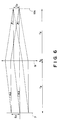
- Figure 6 is a schematic view for further explaining the optical function of the lens system 9 of Figure 1.
- Figure 7 is a schematic view of a portion of a second embodiment of the present invention.
- Figures 8, 9 and 10 are schematic views, respectively, each for explaining a portion of a third embodiment of the present invention.
- Figures 11A and 11B are schematic views, respectively, each for explaining the optical function of the third embodiment.
- Figures 12A and 12B are schematic views, respectively, each for further explaining the optical function of the third embodiment.
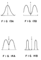
- Figures 13A and 13B are graphs, respectively, each showing an example of light intensity distribution in the third embodiment of the present invention.
- Figures 14A and 14B are graphs, respectively, each showing a further example of light intensity distribution in the third embodiment of the present invention.
- Figures 15A - 15C are schematic views, respectively, each showing a main portion of a fourth embodiment of the present invention.
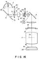
- Figure 16 is a schematic view of a main portion of a fifth embodiment of the present invention.
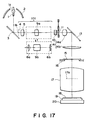
- Figure 17 is a schematic view of a main portion of a sixth embodiment of the present invention.
- Figure 18 is a schematic view for explaining a portion of Figure 17.
- Figure 19 is a schematic view for further explaining a portion of Figure 17.
- Figures 20A - 20C are schematic views, respectively, each for explaining the state of incidence of light upon a light entrance plane 10a of an optical integrator 10 of Figure 17.
- Figure 21 is a schematic view of an apertured stop.
- Figure 22 is a schematic view of a main portion of a seventh embodiment of the present invention.
- Figure 1 is a schematic view of an illumination device and a projection exposure apparatus using the same, according to an embodiment of the present invention.
- the invention is applied to a reduction projection type exposure apparatus, called a stepper.
- This exposure apparatus can be used for manufacture of microdevices such as semiconductor memories, CCDs, liquid crystal panels or magnetic head, for example.
- a light source such as a high luminance ultra high pressure Hg lamp, for example, for emitting ultraviolet light or deep UV light.
- the light source 1 has its light emitting portion 1a disposed adjacent to the first focal point of an elliptical mirror 2.
- the light emanating from the light source 1 is reflected and collected by the elliptical mirror 2, and then it is reflected by a cold mirror 3 by which an image 1b of the light emitting portion 1a (an image of light source) is formed in the neighbourhood of the second focal point 4 of the elliptical mirror 2.
- the cold mirror 3 has a multilayered film and it mainly serves to transmit infrared light but to reflect ultraviolet light.
- Denoted at 101 is an imaging system having two lens systems 5 and 9. It serves to image the light source image 1b, formed in the neighbourhood of the second focal point 4, upon an entrance plane 10a of an optical integrator 10 through the cooperation of an optical device 8.
- the optical device 8 comprises a prism member 6 having a conical prism, for deflecting received light to a predetermined direction, and a parallel flat plate 7 for projecting received light directly.
- Denoted at 8a is a holding member by which the prism member 6 and the parallel plate 7 of the optical device 8 can be alternately and selectively placed on the light path.
- the imaging system 101 is defined as an telecentric system on the exit side.
- the optical device 8 is disposed in the neighbourhood of the pupil plane of the imaging system, where the opening of the elliptical mirror is imaged.
- the optical integrator 10 comprises a plurality of small lenses which are arrayed two-dimensionally, and it serves to define a secondary light source 10c in the neighbourhood of the exit surface 10b thereof.
- Denoted at 11 is a stop member having a plurality of apertures.
- the stop member is provided with a mechanism by which the shape of aperture on the light path can be changed.
- the stop member 11 is disposed in such region in which discrete secondary light source elements do not overlap.
- Denoted at 14a is a lens system for collecting the light from the exit surface 10b of the optical integrator 10 and for illuminating, through the stop member 11 and a mirror 13 as well as a collimator lens 14b, a reticle (surface to be illuminated) 15 placed on a reticle stage 16.
- the lens system 14a and the collimator lens 14b constitute a condensing lens system 14.
- Denoted at 17 is a projection optical system for projecting, in a reduced scale, a pattern formed on the reticle 15 upon the surface of a wafer 18 which is placed on a wafer chuck 19.
- Denoted at 20 is a water stage on which the wafer chuck 19 is mounted.
- an image of the secondary light source 10c formed in the neighbourhood of the exit surface 10b of the optical integrator 10 is formed in the neighbourhood of a pupil 17a of the projection optical system 17.
- Figures 2A and 3A each illustrates the light path from the elliptical mirror 2 ( Figure 1) to the optical integrator 10, the path being extended.
- the mirror 3 is not shown in Figure 2A or 3A.
- the illustrations of Figures 2A - 2C and 3A - 3C explain that the light intensity distribution upon the entrance surface 10a of the optical integrator 10 is changed by alternately selecting the elements 6 and 7 of the optical device 8.
- Figures 2A - 2C correspond to a case where the parallel plate 7 of the optical device 8 is disposed on the light path
- Figures 3A - 3C correspond to a case where the prism member 6 of the optical device 8 is disposed on the light path.
- the illumination system of Figure 2A is adapted for a first state of projection in which a very high resolution is not required but in which a larger depth of focus is assured.
- the illumination system of Figure 3A is adapted for a second state of projection in which a high resolution is required mainly.
- Figures 2C and 3C each is a schematic representation of light intensity distribution upon the light entrance surface 10a of the optical integrator 10.
- the zone depicted by hatching in the drawings denotes the region of higher light intensity, as compared with the remaining region.
- Figures 2B and 3B illustrate distribution of light intensity I along the X-axis direction ( Figure 2C or 3C).
- the parallel plate 7 of the optical device 8 is disposed on the light path, and the light source image 1b as formed at the second focal point 4 of the elliptical mirror 2 is imaged by the imaging system 101 upon the light entrance surface 10a of the optical integrator 10.
- the light intensity distribution in section upon the light entrance surface 10a of the optical integrator 10 has an approximately Gaussian shape which is rotationally symmetric.
- the prism member 6 of the optical device 8 is placed on the light path, and the light source image (point image) 1b formed at the second focal point 4 of the elliptical mirror 2 is imaged, into a ring-like shape, on the light entrance surface 10a of the optical integrator 10 by the imaging system 101.
- the light intensity distribution on the light entrance surface 10a of the integrator 10 has a ring-like shape such as shown in Figures 3B or 3C wherein the light intensity is lower at the optical axis portion but is higher at the peripheral portion. Why this is so will now be explained below.
- Figure 4 schematically illustrates the disposition of the parallel flat plate 7, the lens system 9 and the light entrance surface 10a of the optical integrator 10 of Figure 2A.
- these elements are so disposed that the optical distance between the parallel plate 7 and the forward principal point of the lens system 9 as well as the optical distance between the backward principal point of the lens system 9 and the light entrance surface 10a of the integrator 10 are, if the focal length of the lens system 9 is denoted by f 0 , both equal to a distance f 0 .
- the light intensity distribution on the entrance surface 10a of the integrator 10 is changed into a ring-like intensity distribution having lower intensity at the optical axis portion and higher intensity at the peripheral portion.
- the light intensity distribution on the entrance surface 10a of the integrator 10 corresponds to the light intensity distribution of an effective light source which is defined at the pupil plane 17a of the projection optical system 17, by using the prism member 6 in place of the parallel plate 7 such an effective light source having light intensity distribution having lower intensity at a central portion (optical axis portion) and higher intensity at a peripheral portion is defined on the pupil plane of the projection optical system.
- the stop member 11 is provided in the neighbourhood of the exit surface 10b of the optical integrator 10.
- This stop member has a plurality of apertures and is provided with a mechanism for changing, as desired, the aperture shape thereof.
- the aperture shape which is variable is predetermined and it corresponds to the shape of the secondary light source to be formed at the pupil plane 17a of the projection optical system 17.
- the stop member may have a ring-like aperture of a property for passing a larger quantity of light at its peripheral portion than at its central portion.
- the selection of the prism member 6 of the optical device 8 singly or the selection of the prism member 6 together with the changing the aperture shape of the stop member 11 in combination assures a desired shape of effective light source while a attaining high efficiency of light utilization.
- stop member 11 is not a requisition in this embodiment.
- the structure shown in Figure 2A is selected (like an illumination system of conventional type), whereby a Gaussian shape light intensity distribution is provided at the entrance surface 10a of the optical integrator 10 (first state).
- the structure shown in Figure 3A is selected to provide a ring-like light intensity distribution at the entrance surface 10a of the integrator 10. Also, the aperture shape of the stop member 11 is changed. By this, an illumination device for high resolution projection is assured (second state).
- the insertion of the parallel plate 7 in the first state of Figure 2A is to minimize the difference in optical path length between the lens systems 5 and 9, as compared with that in the case where the prism member 6 is inserted in the second state. If the prism member 6 has a small thickness or is a slight change in optical path length between the lens systems 5 and 9 does not influence the optical performance of the optical integrator 10 or of any other optical elements following it, the parallel plate 7 may be omitted.
- Figures 5 and 6 are schematic representations for explaining the relationship of the incidence height (heights t 1 and t 2 from the optical axis) at the entrance surface 10a of the optical integrator 10, relative to the position (exit heights S 1 and S 2 ) and deflection angle ( ⁇ 1 and ⁇ 2 ) of light passing through the parallel plate 7, where in the present embodiment the focal length f of the lens system 9 constituting the imaging system 101 is changed.
- the focal length of the lens system 9 may be so set to define a prism angle of 5 - 20 deg.
- Figure 7 is a schematic view of a main portion of a second embodiment of the present invention.
- a half mirror 30 is disposed on the light path at the position before (light source 1 side) of the optical integrator 10, so that a portion of the light from the imaging system 101 is directed to a photodetector 31 which may comprise a CCD or a quadrant sensor.
- the remaining portion is of the same structure as of the first embodiment.
- the light intensity distribution at the light entrance surface 10a of the optical integrator 10 is measured indirectly to monitor the same. This allows adjustment of the imaging system 101 while monitoring changes in light intensity and/or light intensity distribution at the entrance surface 10a.
- a mechanism 60 for rotating the optical member 6 about the optical axis or for shifting the same with respect to the optical axis may be used. This enables to change the light intensity distribution at the entrance surface 10a of the integrator 10 into a desired shape easily.
- Figure 8 is a schematic view of a main portion of a third embodiment of the present invention.
- the lens system 9 is replaced by a lens system 33 of a different focal length which is disposed at the entrance face 10a side of the optical integrator 10.
- the remaining portion is of the same structure as of the first embodiment.
- Figures 11A - 12B schematically illustrate the light path from the optical device 8 (prism 6 and parallel plate 7) to the integrator 10.
- Figures 13A, 13B, 14A and 14B show light intensity distribution at the entrance surface 10a of the integrator 10, defined by using the prism member 6 or the parallel plate 7.
- Figure 11A shows the arrangement where in the first embodiment conventional the illumination is to be done.
- the angle of light rays that can enter the optical integrator is determined and, in the example of Figure 11A, the angle is ⁇ 1 .
- the optical system before the integrator 10 is designed so that the angle of incidence upon the integrator 10 becomes not greater than the angle ⁇ .
- the degree of convergence is limited due to Lagrange's invariant. For example, it is not possible to improve the degree of convergence beyond that of Figure 13A. An attempt to obtaining higher degree of convergence simply ends in that the angle of incidence upon the integrator 10 goes beyond the angle ⁇ .
- Figure 11B shows the state where in the first embodiment the prism member 6 is inserted into the light path.
- Figure 13B shows corresponding light intensity distribution at the entrance surface 10a.
- the maximum incidence angle of the light upon the entrance surface 10a, at the point S 1 is ⁇ 1 the same as the Figure 11A example.
- the effective light angle of the light actually enters is ⁇ 2 .
- Figure 14A shows corresponding light intensity distribution at the entrance surface 10a.
- Figure 12B shows an example wherein the degree of convergence is improved on the basis of such optical principle just described.
- Corresponding light intensity distribution is shown in Figure 13B.
- the prism member 6 has an enlarged prism angle so as to obtain light intensity distribution of ring-like shape.
- the insertion of the prism member 6 as described causes shift of the angle of incidence at the entrance surface 10a of the integrator 10 while the maximum incidence angle being unchanged.
- the incidence angle is loosened.
- Figures 15A - 15C are schematic views of a portion of a fourth embodiment of the present invention.
- the position of the optical device 8 (the position of prism member 6 and/or parallel plate 7) is shifted from the pupil of the imaging system 101 and the focal length of the optical system 9 is changed, to thereby converge the light intensity distribution at the entrance surface 10a of the optical integrator 10.
- the remaining portion is of the same structure as of the first embodiment.
- FIGs 15A - 15C reference character P denotes the pupil plane of the lens system 9.
- Figure 15A shows the first state of illumination in the first embodiment.
- the angle of incidence upon the integrator 10 is ⁇ .
- Figure 15B shows the second state of illumination in the first embodiment, and the incidence angle is ⁇ the same as in the Figure 11A example.
- the prism member 6 is shifted from the pupil plane P and the beam diameter on the plane P is reduced such as shown in Figure 15C, then it is possible to make the incidence angle ⁇ ' smaller than the angle ⁇ 2 of the Figure 11A and 11B examples.
- the focal length of the lens system 9 is changed so as to assure that the light intensity distribution at the entrance surface 10a of the integrator 10 is collected and converged locally.
- Figure 16 is a schematic view of a main portion of a fifth embodiment of the present invention.
- the lens system 5 constituting the imaging system 101 is omitted and the opening 2a of the elliptical mirror 2 is imaged by the lens system 9 upon the entrance surface 10a of the optical integrator 10.
- the optical device 8 is disposed in the neighbourhood of the second focal point of the elliptical mirror 2. The remaining portion is of the same structure as of the first embodiment.
- an image of the light emitting portion 1a of the light source 1 is formed on the entrance surface 10a of the integrator 10, and the optical device 8 is disposed in the neighbourhood of the imaging position of the opening 2a of the elliptical mirror 2 (the position of the image of the opening 2a) which is between the light source 1 and the integrator 10.
- the image of the opening 2a of the elliptical mirror 2 is formed on the entrance surface 10a of the integrator 10, and the optical device 8 is disposed at the imaging position of the light emitting portion 1a (the second focal point position of the elliptical mirror 2) which is between the light source 1 and the optical integrator 10.
- the forward focal point position of the lens system 9 is placed substantially at the second focal point position of the elliptical mirror 2, and by the lens system 9, the light from the light source image 1b at the second focal point is transformed into substantially parallel light which is then directed to the entrance surface 10a of the integrator 10. Parallel light from the lens system 9 is projected on the entrance surface 10a of the integrator 10.
- Figure 17 is a schematic view of a main portion of a sixth embodiment of the present invention.
- the optical device 8 comprises at least two prism members 6a and 6b disposed along the optical axis and, for changing the light intensity distribution at the entrance surface 10a of the integrator 10, namely, for rendering the illumination system into the second state, the optical device 8 (prism members 6a and 6b) is mounted on the optical axis and, additionally, a portion of the lens system 9a constituting the imaging system 101 is replaced by another lens system 9b so as to reduce the incidence angle of off-axis principal ray to the entrance surface 10a. This is done for efficient utilization of light.
- the lens system 9a in the first state the lens system 9a is placed on the light path (the optical device 8 is not used), so at to provide light intensity distribution at the entrance surface 10a of the integrator 10, that is, light intensity distribution at the pupil plane 17a of the projection optical system 17, which distribution is of a rotationally symmetric shape wherein the intensity is higher at the central portion than at the peripheral portion.
- the second state is defined by placing the optical device 8 (prism members 6a and 6b) on the light path and by replacing the lens system 9a by the lens system 9b having a different focal length.
- This makes smaller the angle of incidence of the principal ray upon the entrance surface 10a of the integrator 10, whereby at this entrance surface 10a, namely, at the pupil plane 17a of the projection optical system 17, such light intensity distribution in which the intensity is higher in the peripheral portion than in the central portion is provided.
- lens system 5 collects the light from the light source image 1b formed in the neighbourhood of the second focal point 4, and it emits parallel light.
- the imaging system 101 (lens systems 5 and 9a) is telecentric on the exit side. At least a portion of the collecting lens 14 is made movable along the optical axis, to adjust the light intensity distribution on the reticle 15.
- the lens system 9a which is a constituent element of the imaging system 101 is replaced by the optical device 8 (including two prisms 6a and 6b) and the lens system 9b, to change the light intensity distribution at the entrance surface 10a of the integrator 10.
- the aperture shape of the stop member 11 is changed to change the light intensity distribution of the image of the secondary light source which image is formed at the pupil plane 17a of the projection optical system 17.
- Figures 18 and 19 each schematically illustrate the light path from the elliptical mirror 2 to the optical integrator 10 of Figure 17, the path being extended.
- the mirror 3 is not shown in Figure 18 or 19.
- the illustrations of Figures 18 and 19 explain that the components of the optical device 8 are interchanged to change the light intensity distribution on the entrance surface 10a of the integrator 10.
- Figure 18 shows the state in which the lens system 9a is placed on the light path.
- Figure 19 shows the state in which the lens system 9a is removed and, in place thereof, the prism members 6a and 6b of the optical device 8 and the lens system 9b are placed on the light path.
- the illumination system of Figure 18 is in the first state of projection in which a very high resolution is not required but a large depth of focus is assured, as in the illumination method of conventional type.
- the illumination system of Figure 19 is in the second state of projection, according to the present invention, mainly for attaining high resolution.
- the portion (B) of Figure 18 and the portion (B) of Figure 19 schematically each shows corresponding light intensity distribution on the entrance surface 10a of the integrator 10.
- the zone depicted by hatching denotes the region of higher intensity as compared with the remaining region.
- the distribution of light intensity I along the X-axis direction are depicted.
- Figures 20A, 20B and 20C are schematic representations, for explaining the light rays impinging on the optical integrator 10, in the systems of Figure 18 and 19.
- Reference characters + ⁇ and - ⁇ each denotes the range (angle) of light rays that can enter the optical integrator 10 (that can emerge from the integrator without being eclipsed).
- Grid portion in each illustration depicts the zone in which the light intensity is higher than that of the light entering the integrator 10.
- Figure 18, (A) shows the optical arrangement in ordinary illumination.
- the light intensity distribution at the entrance face 10a of the integrator 10 is like a Gaussian distribution such as shown in Figure 18, (B).
- the incidence angle thereof is such as shown in Figure 20A.
- a stop 121 having an aperture 121a such as shown in Figure 21 is inserted at the back of or in front of the integrator 10.
- this method only the light in the hatched zone of the light intensity distribution of Figure 18, (A), can be used and, therefore, the illuminance decreases considerably.
- the lens system 9a is replaced by the lens system 9b of smaller focal length (the optical components are disposed so that, if the focal length of the lens system 9b is f 9b , the optical distance between the prism 6a and the lens system 9b and the optical distance between the lens system 9b and the entrance surface 10a of the integrator 10 are both equal to f 9b ), such that the light intensity distribution as shown in Figure 19, (B), is provided at the entrance surface 10a of the integrator 10.
- the prism member 6b having an appropriate prism angle is inserted in front of the integrator 10, by which the incidence angle of light rays (incidence angle of off-axis light) is made smaller such as shown in Figure 20C. This assures efficient impingement or entrance of light into the integrator 10. '£hus, almost all the input light can be used for the illumination.
- the present embodiment uses the optical arrangement such as shown in Figure 19, (A), by which illumination for high resolution is assured without a substantial loss of illuminance at the surface to be illuminated.
- the prism member 6a or 6b provided within the imaging system 101 is a conical prism.
- the lens elements of the lens system 9a may be displaced (like a zoom lens system) to define the same condition as by the lens system 9b. Only some of the lens elements may be moved like a zoom lens system or, alternatively, some lens elements may be replaced by different lens elements.
- the stop member 121 for high resolution such as shown in Figure 21 may be used as desired, or it may be omitted.
- the focal length of the lens system 9a is changed to change the magnification of the imaging system 101
- the focal length of the lens system 5 may be changed.
- both of the focal lengths of the lens systems 5 and 9 may be changed.
- an additional imaging system may be disposed between the optical system 14 and the reticle such that a plane which is optically conjugate with the reticle 15 surface with respect to the additional imaging system may be illuminated.
- Figure 22 is a schematic view of a main portion of a seventh embodiment of the present invention.
- a half mirror 43 is disposed between the integrator 10 and the surface 15 to be illuminated, so as to allow detection of the amount of exposure of the surface being illuminated.
- the remaining portion is of substantially the same structure as of the first embodiment.
- denoted at 44 is the reticle pattern surface or a plane which is optically conjugate with the reticle pattern surface.
- Denoted at 45 is a pinhole member which is disposed at a position optically conjugate with the plane 44.
- Denoted at 33 is a photosensor (e.g., CCD or quadrant sensor).
- the half mirror 43 is placed between the lens system 13a and the collimator lens 14b, it may be disposed at any position between the integrator 10 and the surface 15.
- an illumination system suited to such pattern in consideration of fineness and/or orientation of a pattern of a reticle to be projected and transferred, an illumination system suited to such pattern can be selected.
Landscapes
- Physics & Mathematics (AREA)
- General Physics & Mathematics (AREA)
- Exposure And Positioning Against Photoresist Photosensitive Materials (AREA)
- Exposure Of Semiconductors, Excluding Electron Or Ion Beam Exposure (AREA)
- Eye Examination Apparatus (AREA)
- Non-Portable Lighting Devices Or Systems Thereof (AREA)
- Photographic Developing Apparatuses (AREA)
- Light Sources And Details Of Projection-Printing Devices (AREA)
Claims (17)
- Beleuchtungssystem, wobei Licht von einer primären Lichtquelle (1) auf einen optischen Integrator (10) projiziert wird, wodurch eine sekundäre Lichtquelle ausgebildet wird, und wobei Lichter von der sekundären Lichtquelle auf eine Oberfläche projiziert werden, die von einem optischen System (13,14) zu beleuchten ist (15;18), wobei sie miteinander überlagert werden,
dadurch gekennzeichnet, daß
sich ein Ablenkteil (6) mit einer konischen, Licht ablenkenden Oberfläche entfernbar zwischen der primären Lichtquelle (1) und dem optischen Integrator (10) befindet, wobei das Ablenkteil der Umwandlung des Lichts von der primären Lichtquelle (1) in ein ringförmiges Lichtmuster dient, das auf den optischen Integrator (10) projiziert wird, um eine ringförmige, sekundäre Lichtquelle auszubilden, wenn das Ablenkteil (6) vorhanden ist. - System nach Anspruch 1, ferner
dadurch gekennzeichnet, daß
ein optisches Abbildungssystem (2, 3, 5, 9) einschließlich einer Kollimatorlinse (5) und einer Sammellinse (9) zum Abbilden der primären Lichtquelle (1) auf den optischen Integrator (10) bereitgestellt ist, wobei das Ablenkteil in einem Weg des parallelen Lichts zwisehen der Kollimatorlinse (5) und der Sammellinse (9) entfernbar untergebracht ist. - System nach Anspruch 2, wobei das optische Abbildungssystem eine variable Abbildungsvergrößerung aufweist.
- System nach Anspruch 3, wobei die Sammellinse (9) eines von mehreren Linsensystemen (9, 33; 9a, 9b) darstellt, die austauschbar verwendbar sind, und wobei die Abbildungsvergrößerung durch Ändern des Linsensystems geändert werden kann.
- System nach Anspruch 3, wobei das optische Abbildungssystem (2, 3, 5, 9) eine kontinuierliche Brennweitenverstellungsfunktion aufweist.
- System nach einem der Ansprüche 1 - 5, ferner mit einer Bewegungseinrichtung (600) zum Bewegen des Ablenkteils (6) in eine Richtung, die eine optische Achse kreuzt.
- System nach einem der Ansprüche 1 - 6, wobei ein zweites Ablenkteil (32; 6b) zwischen der Sammellinse (9) und dem optischen Integrator (10) bereitgestellt ist, um den Einfallswinkel des ringförmigen Lichts auf den optischen Integrator zu reduzieren.
- System nach Anspruch 7, wobei das zweite Ablenkteil eine Feldlinse (32) aufweist.
- System nach Anspruch 7, wobei das zweite Ablenkteil ein konisches Prisma (6b) aufweist.
- System nach Anspruch 1, ferner
gekennzeichnet durch
einen elliptischen Spiegel (2) zur Reflexion von Licht von der primären Lichtquelle (1) und ein zweites optisches System (9) zur Projektion des Bildes der primären Lichtquelle auf den optischen Integrator (10) mittels des elliptischen Spiegels, wobei das Ablenkteil (6) zwischen dem zweiten optischen Teil (9) und dem Bild (lb) der primären Lichtquelle entfernbar untergebracht ist. - System nach einem der Ansprüche 1 - 10, wobei das Ablenkteil ein konisches Prisma (6) aufweist.
- System nach einem der Ansprüche 1 - 11, wobei es ein Stopteil (11) gibt, das einen Stop bei einer Öffnung außerhalb der optischen Achse vorsieht, um die Form der sekundären Lichtquelle zu definieren.
- System nach Anspruch 12, wobei das Stopteil (11) eine Funktion des Variierens der Form der Öffnung aufweist.
- System nach einem der Ansprüche 1 - 12, wobei es eine Korrektureinrichtung (14) gibt, um eine Beleuchtungsungleichförmigkeit auf der zu beleuchtenden Oberfläche (15, 18) zu korrigieren.
- System nach einem der Ansprüche 1 - 12, das eine Meßeinrichtung (30, 31) zur Messung einer Lichtintensitätsverteilung auf dem optischen Integrator (10) aufweist.
- Projektionsbelichtungsgerät mit einem Beleuchtungssystem nach einem der Ansprüche 1 - 15, und einem optischen Projektionssystem (17) zur Projektion eines Musters einer Maske, das von dem Beleuchtungssystem auf das Substrat (18) geleuchtet wird.
- Verfahren zur Herstellung einer Mikrovorrichtung, mit den SchrittenÜbertragen eines Schaltungsmusters auf ein Substrat unter Verwendung eines Projektionsbelichtungsgerätes nach Anspruch 16, undVerarbeiten des Substrats, um eine funktionsfähige Mikrovorrichtung entsprechend dem projizierten Muster zu realisieren.
Applications Claiming Priority (3)
| Application Number | Priority Date | Filing Date | Title |
|---|---|---|---|
| JP108632/92 | 1992-03-31 | ||
| JP10863292 | 1992-03-31 | ||
| JP10863292A JP3278896B2 (ja) | 1992-03-31 | 1992-03-31 | 照明装置及びそれを用いた投影露光装置 |
Publications (2)
| Publication Number | Publication Date |
|---|---|
| EP0564264A1 EP0564264A1 (de) | 1993-10-06 |
| EP0564264B1 true EP0564264B1 (de) | 1999-10-06 |
Family
ID=14489725
Family Applications (1)
| Application Number | Title | Priority Date | Filing Date |
|---|---|---|---|
| EP93302508A Expired - Lifetime EP0564264B1 (de) | 1992-03-31 | 1993-03-31 | Beleuchtungsvorrichtung für einen Projektionsbelichtungsapparat |
Country Status (5)
| Country | Link |
|---|---|
| US (2) | US5345292A (de) |
| EP (1) | EP0564264B1 (de) |
| JP (1) | JP3278896B2 (de) |
| AT (1) | ATE185429T1 (de) |
| DE (1) | DE69326630T2 (de) |
Families Citing this family (85)
| Publication number | Priority date | Publication date | Assignee | Title |
|---|---|---|---|---|
| US6411377B1 (en) * | 1991-04-02 | 2002-06-25 | Hitachi, Ltd. | Optical apparatus for defect and particle size inspection |
| US5424803A (en) * | 1991-08-09 | 1995-06-13 | Canon Kabushiki Kaisha | Projection exposure apparatus and semiconductor device manufacturing method |
| JPH0567558A (ja) * | 1991-09-06 | 1993-03-19 | Nikon Corp | 露光方法 |
| US6078380A (en) * | 1991-10-08 | 2000-06-20 | Nikon Corporation | Projection exposure apparatus and method involving variation and correction of light intensity distributions, detection and control of imaging characteristics, and control of exposure |
| JP3278896B2 (ja) * | 1992-03-31 | 2002-04-30 | キヤノン株式会社 | 照明装置及びそれを用いた投影露光装置 |
| NL194929C (nl) * | 1992-10-20 | 2003-07-04 | Samsung Electronics Co Ltd | Projectiebelichtingssysteem. |
| JP3316937B2 (ja) * | 1992-11-24 | 2002-08-19 | 株式会社ニコン | 照明光学装置、露光装置、及び該露光装置を用いた転写方法 |
| JP2894922B2 (ja) * | 1993-05-14 | 1999-05-24 | 日本電気株式会社 | 投影露光方法および装置 |
| US5552856A (en) * | 1993-06-14 | 1996-09-03 | Nikon Corporation | Projection exposure apparatus |
| JP3291849B2 (ja) * | 1993-07-15 | 2002-06-17 | 株式会社ニコン | 露光方法、デバイス形成方法、及び露光装置 |
| JP3275575B2 (ja) * | 1993-10-27 | 2002-04-15 | キヤノン株式会社 | 投影露光装置及び該投影露光装置を用いたデバイスの製造方法 |
| JP3057998B2 (ja) * | 1994-02-16 | 2000-07-04 | キヤノン株式会社 | 照明装置及びそれを用いた投影露光装置 |
| JP3456597B2 (ja) * | 1994-04-14 | 2003-10-14 | 株式会社ニコン | 露光装置 |
| EP0687956B2 (de) | 1994-06-17 | 2005-11-23 | Carl Zeiss SMT AG | Beleuchtungseinrichtung |
| JP3060357B2 (ja) * | 1994-06-22 | 2000-07-10 | キヤノン株式会社 | 走査型露光装置及び該走査型露光装置を用いてデバイスを製造する方法 |
| JP3458549B2 (ja) | 1994-08-26 | 2003-10-20 | ソニー株式会社 | パターン形成方法および該方法を用いた半導体デバイス製造方法と装置 |
| KR100210569B1 (ko) * | 1995-09-29 | 1999-07-15 | 미따라이 하지메 | 노광방법 및 노광장치, 그리고 이를 이용한 디바이스제조방법 |
| JPH10153866A (ja) * | 1996-11-22 | 1998-06-09 | Nikon Corp | 照明装置および該照明装置を備えた露光装置 |
| US6628370B1 (en) | 1996-11-25 | 2003-09-30 | Mccullough Andrew W. | Illumination system with spatially controllable partial coherence compensating for line width variances in a photolithographic system |
| US6259513B1 (en) * | 1996-11-25 | 2001-07-10 | Svg Lithography Systems, Inc. | Illumination system with spatially controllable partial coherence |
| DE19653983A1 (de) | 1996-12-21 | 1998-06-25 | Zeiss Carl Fa | REMA-Objektiv für Mikrolithographie-Projektionsbelichtungsanlagen |
| US7130129B2 (en) | 1996-12-21 | 2006-10-31 | Carl Zeiss Smt Ag | Reticle-masking objective with aspherical lenses |
| US5981954A (en) * | 1997-01-16 | 1999-11-09 | Canon Kabushiki Kaisha | Electron beam exposure apparatus |
| JP3689516B2 (ja) * | 1997-01-29 | 2005-08-31 | キヤノン株式会社 | 電子ビーム露光装置 |
| JPH10214779A (ja) * | 1997-01-31 | 1998-08-11 | Canon Inc | 電子ビーム露光方法及び該方法を用いたデバイス製造方法 |
| US6107636A (en) | 1997-02-07 | 2000-08-22 | Canon Kabushiki Kaisha | Electron beam exposure apparatus and its control method |
| US6027865A (en) * | 1997-02-10 | 2000-02-22 | Texas Instruments Incorporated | Method for accurate patterning of photoresist during lithography process |
| EP0874283B1 (de) * | 1997-04-23 | 2003-09-03 | Nikon Corporation | Optischer Belichtungsapparat und optisches Reinigungsverfahren |
| JP3787417B2 (ja) * | 1997-06-11 | 2006-06-21 | キヤノン株式会社 | 電子ビーム露光方法及び電子ビーム露光装置 |
| AU8356298A (en) * | 1997-07-22 | 1999-02-16 | Nikon Corporation | Projection exposure method, projection aligner, and methods of manufacturing andoptically cleaning the aligner |
| JP3264224B2 (ja) | 1997-08-04 | 2002-03-11 | キヤノン株式会社 | 照明装置及びそれを用いた投影露光装置 |
| AU1262799A (en) * | 1997-12-05 | 1999-06-28 | Nikon Corporation | Exposure method and exposure device |
| EP0949541B1 (de) * | 1998-04-08 | 2006-06-07 | ASML Netherlands B.V. | Lithographischer Apparat |
| DE69931690T2 (de) * | 1998-04-08 | 2007-06-14 | Asml Netherlands B.V. | Lithographischer Apparat |
| DE19830438A1 (de) * | 1998-07-08 | 2000-01-13 | Zeiss Carl Fa | Verfahren zur Dekontamination von Mikrolithographie-Projektionsbelichtungsanlagen |
| US6480263B1 (en) * | 1998-10-22 | 2002-11-12 | Asml Netherlands B.V. | Apparatus and method for phase shift photomasking |
| US6563567B1 (en) * | 1998-12-17 | 2003-05-13 | Nikon Corporation | Method and apparatus for illuminating a surface using a projection imaging apparatus |
| US6392742B1 (en) | 1999-06-01 | 2002-05-21 | Canon Kabushiki Kaisha | Illumination system and projection exposure apparatus |
| US6600550B1 (en) | 1999-06-03 | 2003-07-29 | Nikon Corporation | Exposure apparatus, a photolithography method, and a device manufactured by the same |
| US6867922B1 (en) | 1999-06-14 | 2005-03-15 | Canon Kabushiki Kaisha | Projection optical system and projection exposure apparatus using the same |
| JP3359302B2 (ja) | 1999-06-14 | 2002-12-24 | キヤノン株式会社 | 投影露光装置 |
| JP2000356741A (ja) | 1999-06-14 | 2000-12-26 | Canon Inc | 投影光学系 |
| JP4717974B2 (ja) | 1999-07-13 | 2011-07-06 | 株式会社ニコン | 反射屈折光学系及び該光学系を備える投影露光装置 |
| TW587199B (en) | 1999-09-29 | 2004-05-11 | Asml Netherlands Bv | Lithographic method and apparatus |
| JP2001343589A (ja) * | 2000-03-31 | 2001-12-14 | Canon Inc | 投影光学系、および該投影光学系による投影露光装置、デバイス製造方法 |
| JP3927753B2 (ja) | 2000-03-31 | 2007-06-13 | キヤノン株式会社 | 露光装置及びデバイス製造方法 |
| JP4545874B2 (ja) * | 2000-04-03 | 2010-09-15 | キヤノン株式会社 | 照明光学系、および該照明光学系を備えた露光装置と該露光装置によるデバイスの製造方法 |
| JP2001326171A (ja) * | 2000-05-18 | 2001-11-22 | Canon Inc | 照明装置 |
| US6879390B1 (en) * | 2000-08-10 | 2005-04-12 | Kla-Tencor Technologies Corporation | Multiple beam inspection apparatus and method |
| CN100397557C (zh) * | 2001-12-17 | 2008-06-25 | 赛博光学半导体公司 | 半导体晶片载体映射传感器 |
| US6888615B2 (en) * | 2002-04-23 | 2005-05-03 | Asml Holding N.V. | System and method for improving linewidth control in a lithography device by varying the angular distribution of light in an illuminator as a function of field position |
| JP3950732B2 (ja) * | 2002-04-23 | 2007-08-01 | キヤノン株式会社 | 照明光学系、照明方法及び露光装置 |
| JP3950731B2 (ja) * | 2002-04-23 | 2007-08-01 | キヤノン株式会社 | 照明光学系、当該照明光学系を有する露光装置及びデバイス製造方法 |
| JP4235410B2 (ja) | 2002-08-01 | 2009-03-11 | キヤノン株式会社 | 露光方法 |
| KR20170018113A (ko) | 2003-04-09 | 2017-02-15 | 가부시키가이샤 니콘 | 노광 방법 및 장치, 그리고 디바이스 제조 방법 |
| EP1469347A1 (de) * | 2003-04-17 | 2004-10-20 | ASML Netherlands B.V. | Lithographischer Projektionsapparat und Verfahren zur Herstellung einer Vorrichtung |
| JP2004343082A (ja) * | 2003-04-17 | 2004-12-02 | Asml Netherlands Bv | 凹面および凸面を含む集光器を備えたリトグラフ投影装置 |
| DE10322375A1 (de) * | 2003-05-13 | 2004-12-02 | Carl Zeiss Smt Ag | Polarisationsoptimiertes Axiconsystem und Beleuchtungssystem mit einem solchen Axiconsystem |
| US7511886B2 (en) | 2003-05-13 | 2009-03-31 | Carl Zeiss Smt Ag | Optical beam transformation system and illumination system comprising an optical beam transformation system |
| JP2004347777A (ja) * | 2003-05-21 | 2004-12-09 | Olympus Corp | 全反射蛍光顕微鏡 |
| JP3977311B2 (ja) | 2003-10-10 | 2007-09-19 | キヤノン株式会社 | 照明装置及び当該照明装置を有する露光装置 |
| TW201834020A (zh) * | 2003-10-28 | 2018-09-16 | 日商尼康股份有限公司 | 照明光學裝置、曝光裝置、曝光方法以及元件製造方法 |
| TW201809801A (zh) | 2003-11-20 | 2018-03-16 | 日商尼康股份有限公司 | 光學照明裝置、曝光裝置、曝光方法、以及元件製造方法 |
| US7542217B2 (en) * | 2003-12-19 | 2009-06-02 | Carl Zeiss Smt Ag | Beam reshaping unit for an illumination system of a microlithographic projection exposure apparatus |
| US20070019179A1 (en) | 2004-01-16 | 2007-01-25 | Damian Fiolka | Polarization-modulating optical element |
| US8270077B2 (en) | 2004-01-16 | 2012-09-18 | Carl Zeiss Smt Gmbh | Polarization-modulating optical element |
| CN101793993B (zh) | 2004-01-16 | 2013-04-03 | 卡尔蔡司Smt有限责任公司 | 光学元件、光学布置及系统 |
| TWI395068B (zh) | 2004-01-27 | 2013-05-01 | 尼康股份有限公司 | 光學系統、曝光裝置以及曝光方法 |
| TWI389174B (zh) | 2004-02-06 | 2013-03-11 | 尼康股份有限公司 | 偏光變換元件、光學照明裝置、曝光裝置以及曝光方法 |
| US7324280B2 (en) * | 2004-05-25 | 2008-01-29 | Asml Holding N.V. | Apparatus for providing a pattern of polarization |
| US7274434B2 (en) * | 2004-11-24 | 2007-09-25 | Asml Netherlands B.V. | Lithographic apparatus and device manufacturing method |
| JP2006303196A (ja) * | 2005-04-20 | 2006-11-02 | Canon Inc | 測定装置及びそれを有する露光装置 |
| EP2660854B1 (de) | 2005-05-12 | 2017-06-21 | Nikon Corporation | Optisches Projektionssystem, Belichtungsvorrichtung und Belichtungsverfahren |
| JP2006324311A (ja) * | 2005-05-17 | 2006-11-30 | Canon Inc | 波面収差測定装置及びそれを有する露光装置 |
| WO2007022922A2 (de) | 2005-08-23 | 2007-03-01 | Carl Zeiss Smt Ag | Austauschvorrichtung für ein optisches element |
| US20070109520A1 (en) * | 2005-11-17 | 2007-05-17 | Whitney Theodore R | Modular illuminator for a scanning printer |
| JP2008181980A (ja) | 2007-01-23 | 2008-08-07 | Canon Inc | 照明装置の光強度分布の調整方法及び評価方法、照明装置、露光装置及びデバイス製造方法 |
| TWM324785U (en) * | 2007-04-16 | 2008-01-01 | Young Optics Inc | Illumination system |
| JP5267029B2 (ja) | 2007-10-12 | 2013-08-21 | 株式会社ニコン | 照明光学装置、露光装置及びデバイスの製造方法 |
| US8379187B2 (en) | 2007-10-24 | 2013-02-19 | Nikon Corporation | Optical unit, illumination optical apparatus, exposure apparatus, and device manufacturing method |
| US9116346B2 (en) | 2007-11-06 | 2015-08-25 | Nikon Corporation | Illumination apparatus, illumination method, exposure apparatus, and device manufacturing method |
| US20090257043A1 (en) * | 2008-04-14 | 2009-10-15 | Nikon Corporation | Illumination optical system, exposure apparatus, device manufacturing method, and exposure optical system |
| JP2010087388A (ja) * | 2008-10-02 | 2010-04-15 | Ushio Inc | 露光装置 |
| US9235134B2 (en) * | 2010-08-16 | 2016-01-12 | Micron Technology, Inc. | Lens heating compensation in photolithography |
| JP2014056139A (ja) * | 2012-09-13 | 2014-03-27 | Ricoh Co Ltd | 画像投影装置 |
Family Cites Families (43)
| Publication number | Priority date | Publication date | Assignee | Title |
|---|---|---|---|---|
| IT939738B (it) * | 1970-08-12 | 1973-02-10 | Rank Organisation Ltd | Dispositivo di illuminazione per la stampa fotolitografica dei componenti di microcircuiti |
| US3887816A (en) * | 1973-04-26 | 1975-06-03 | Litton Medical Products | Optical system for x-ray scanning equipment |
| DE2835363A1 (de) * | 1978-08-11 | 1980-03-13 | Siemens Ag | Verfahren zum uebertragen von strukturen fuer halbleiterschaltungen |
| JPS5681813A (en) * | 1979-12-08 | 1981-07-04 | Nippon Telegr & Teleph Corp <Ntt> | Mask lighting optical system |
| JPS5825638A (ja) * | 1981-08-08 | 1983-02-15 | Canon Inc | 露光装置 |
| US4498742A (en) * | 1981-09-10 | 1985-02-12 | Nippon Kogaku K.K. | Illumination optical arrangement |
| JPS5843416A (ja) * | 1981-09-10 | 1983-03-14 | Nippon Kogaku Kk <Nikon> | ミラ−集光型逆エキスパンドアフオ−カル照明光学系 |
| JPS58160914A (ja) * | 1982-03-18 | 1983-09-24 | Nippon Kogaku Kk <Nikon> | ミラ−集光型照明光学系 |
| JPS58147708A (ja) * | 1982-02-26 | 1983-09-02 | Nippon Kogaku Kk <Nikon> | 照明用光学装置 |
| JPS59100805A (ja) * | 1982-12-01 | 1984-06-11 | Canon Inc | 物体観察装置 |
| JPS59141226A (ja) * | 1983-02-02 | 1984-08-13 | Canon Inc | 観察装置 |
| JPS59143146A (ja) * | 1983-02-07 | 1984-08-16 | Nippon Kogaku Kk <Nikon> | ミラ−集光型照明光学系 |
| US5091744A (en) * | 1984-02-13 | 1992-02-25 | Canon Kabushiki Kaisha | Illumination optical system |
| US4619508A (en) * | 1984-04-28 | 1986-10-28 | Nippon Kogaku K. K. | Illumination optical arrangement |
| JPH0682598B2 (ja) * | 1984-10-11 | 1994-10-19 | 日本電信電話株式会社 | 投影露光装置 |
| FR2572515B1 (fr) * | 1984-10-25 | 1993-06-18 | Canon Kk | Dispositif de detection de position |
| JPH0782981B2 (ja) * | 1986-02-07 | 1995-09-06 | 株式会社ニコン | 投影露光方法及び装置 |
| US4939630A (en) * | 1986-09-09 | 1990-07-03 | Nikon Corporation | Illumination optical apparatus |
| DE3750174T2 (de) * | 1986-10-30 | 1994-11-17 | Canon K.K., Tokio/Tokyo | Belichtungseinrichtung. |
| JPH0786647B2 (ja) * | 1986-12-24 | 1995-09-20 | 株式会社ニコン | 照明装置 |
| US4902899A (en) * | 1987-06-01 | 1990-02-20 | International Business Machines Corporation | Lithographic process having improved image quality |
| JPS6461716A (en) * | 1987-08-31 | 1989-03-08 | Canon Kk | Illuminator |
| DE68924303T2 (de) * | 1988-06-14 | 1996-02-29 | Nippon Electric Co | Optische Kopfanordnung. |
| JP2699433B2 (ja) * | 1988-08-12 | 1998-01-19 | 株式会社ニコン | 投影型露光装置及び投影露光方法 |
| US4924257A (en) * | 1988-10-05 | 1990-05-08 | Kantilal Jain | Scan and repeat high resolution projection lithography system |
| JPH0812843B2 (ja) * | 1989-03-15 | 1996-02-07 | 日本精工株式会社 | 光学結像装置及び方法 |
| US5153773A (en) * | 1989-06-08 | 1992-10-06 | Canon Kabushiki Kaisha | Illumination device including amplitude-division and beam movements |
| EP0437376B1 (de) * | 1990-01-12 | 1997-03-19 | Sony Corporation | Phasenverschiebungsmaske und Verfahren zur Herstellung |
| US5144362A (en) * | 1990-11-14 | 1992-09-01 | Mitsubishi Denki Kabushiki Kaisha | Projection aligner |
| JP3360686B2 (ja) * | 1990-12-27 | 2002-12-24 | 株式会社ニコン | 照明光学装置および投影露光装置並びに露光方法および素子製造方法 |
| US5305054A (en) * | 1991-02-22 | 1994-04-19 | Canon Kabushiki Kaisha | Imaging method for manufacture of microdevices |
| JPH0541342A (ja) * | 1991-08-05 | 1993-02-19 | Nippon Telegr & Teleph Corp <Ntt> | 微細パタン投影露光装置 |
| JP2673915B2 (ja) * | 1991-05-24 | 1997-11-05 | 日本電信電話株式会社 | 微細パタン投影露光装置 |
| JPH04369209A (ja) * | 1991-06-17 | 1992-12-22 | Nikon Corp | 露光用照明装置 |
| JP3243818B2 (ja) * | 1992-02-14 | 2002-01-07 | 株式会社ニコン | 投影露光装置及び方法、並びに素子製造方法 |
| JP3230264B2 (ja) * | 1992-02-03 | 2001-11-19 | 株式会社ニコン | 投影露光装置及び方法、並びに素子製造方法 |
| JP2803934B2 (ja) * | 1991-12-10 | 1998-09-24 | 三菱電機株式会社 | 投影露光装置及び露光方法 |
| JP2677731B2 (ja) * | 1991-12-17 | 1997-11-17 | 三菱電機株式会社 | 投影露光装置 |
| JP3075381B2 (ja) * | 1992-02-17 | 2000-08-14 | 株式会社ニコン | 投影露光装置及び転写方法 |
| US5309198A (en) * | 1992-02-25 | 1994-05-03 | Nikon Corporation | Light exposure system |
| JP3295956B2 (ja) * | 1992-03-05 | 2002-06-24 | 株式会社ニコン | 露光装置及び半導体素子の製造方法 |
| JP3278896B2 (ja) * | 1992-03-31 | 2002-04-30 | キヤノン株式会社 | 照明装置及びそれを用いた投影露光装置 |
| US5333035A (en) * | 1992-05-15 | 1994-07-26 | Nikon Corporation | Exposing method |
-
1992
- 1992-03-31 JP JP10863292A patent/JP3278896B2/ja not_active Expired - Fee Related
-
1993
- 1993-03-31 EP EP93302508A patent/EP0564264B1/de not_active Expired - Lifetime
- 1993-03-31 AT AT93302508T patent/ATE185429T1/de not_active IP Right Cessation
- 1993-03-31 US US08/040,991 patent/US5345292A/en not_active Expired - Lifetime
- 1993-03-31 DE DE69326630T patent/DE69326630T2/de not_active Expired - Lifetime
-
1995
- 1995-06-05 US US08/461,751 patent/US5726740A/en not_active Expired - Lifetime
Also Published As
| Publication number | Publication date |
|---|---|
| US5345292A (en) | 1994-09-06 |
| DE69326630D1 (de) | 1999-11-11 |
| JP3278896B2 (ja) | 2002-04-30 |
| EP0564264A1 (de) | 1993-10-06 |
| US5726740A (en) | 1998-03-10 |
| ATE185429T1 (de) | 1999-10-15 |
| DE69326630T2 (de) | 2000-04-06 |
| JPH05283317A (ja) | 1993-10-29 |
Similar Documents
| Publication | Publication Date | Title |
|---|---|---|
| EP0564264B1 (de) | Beleuchtungsvorrichtung für einen Projektionsbelichtungsapparat | |
| EP0576297B1 (de) | Vorrichtung zur Senkrechten oder Schrägeinfallenden Beleuchtung einer Maske | |
| US6259512B1 (en) | Illumination system and exposure apparatus having the same | |
| EP0783135B1 (de) | Bilderzeugungsgerät und -Verfahren zur Herstellung von Mikrovorrichtungen | |
| US5673102A (en) | Image farming and microdevice manufacturing method and exposure apparatus in which a light source includes four quadrants of predetermined intensity | |
| EP0867772B1 (de) | Beleuchtungssystem und Belichtungsapparat | |
| JP3559330B2 (ja) | レチクルマスキングシステムを有する光学系の照明手段 | |
| US5719617A (en) | Illumination system for superposing light beams one upon another on a surface using a projecting system having different focal point positions | |
| US20010043318A1 (en) | Illumination optical system for use in projection exposure apparatus | |
| US6857764B2 (en) | Illumination optical system and exposure apparatus having the same | |
| US6323937B1 (en) | Projection exposure apparatus, and device manufacturing method using the same | |
| US6285440B1 (en) | Illumination system and projection exposure apparatus using the same | |
| JP2002198309A (ja) | 熱的な負荷の少ない照明系 | |
| US7242457B2 (en) | Exposure apparatus and exposure method, and device manufacturing method using the same | |
| JP2673915B2 (ja) | 微細パタン投影露光装置 | |
| JP3323863B2 (ja) | 投影露光装置及び半導体素子の製造方法 | |
| JP3548567B2 (ja) | 投影露光装置及び半導体素子の製造方法 | |
| JP3459826B2 (ja) | 投影露光装置及び半導体素子の製造方法 | |
| HK1101221B (en) | Lighting optical device, exposure system, and exposure method | |
| HK1101221A1 (zh) | 照明光学装置、曝光装置和曝光方法 |
Legal Events
| Date | Code | Title | Description |
|---|---|---|---|
| PUAI | Public reference made under article 153(3) epc to a published international application that has entered the european phase |
Free format text: ORIGINAL CODE: 0009012 |
|
| AK | Designated contracting states |
Kind code of ref document: A1 Designated state(s): AT BE CH DE DK ES FR GB GR IE IT LI LU MC NL PT SE |
|
| 17P | Request for examination filed |
Effective date: 19940223 |
|
| 17Q | First examination report despatched |
Effective date: 19960508 |
|
| GRAG | Despatch of communication of intention to grant |
Free format text: ORIGINAL CODE: EPIDOS AGRA |
|
| GRAG | Despatch of communication of intention to grant |
Free format text: ORIGINAL CODE: EPIDOS AGRA |
|
| GRAG | Despatch of communication of intention to grant |
Free format text: ORIGINAL CODE: EPIDOS AGRA |
|
| GRAH | Despatch of communication of intention to grant a patent |
Free format text: ORIGINAL CODE: EPIDOS IGRA |
|
| GRAH | Despatch of communication of intention to grant a patent |
Free format text: ORIGINAL CODE: EPIDOS IGRA |
|
| GRAA | (expected) grant |
Free format text: ORIGINAL CODE: 0009210 |
|
| AK | Designated contracting states |
Kind code of ref document: B1 Designated state(s): AT BE CH DE DK ES FR GB GR IE IT LI LU MC NL PT SE |
|
| PG25 | Lapsed in a contracting state [announced via postgrant information from national office to epo] |
Ref country code: SE Free format text: THE PATENT HAS BEEN ANNULLED BY A DECISION OF A NATIONAL AUTHORITY Effective date: 19991006 Ref country code: LI Free format text: LAPSE BECAUSE OF FAILURE TO SUBMIT A TRANSLATION OF THE DESCRIPTION OR TO PAY THE FEE WITHIN THE PRESCRIBED TIME-LIMIT Effective date: 19991006 Ref country code: IT Free format text: LAPSE BECAUSE OF FAILURE TO SUBMIT A TRANSLATION OF THE DESCRIPTION OR TO PAY THE FEE WITHIN THE PRE;WARNING: LAPSES OF ITALIAN PATENTS WITH EFFECTIVE DATE BEFORE 2007 MAY HAVE OCCURRED AT ANY TIME BEFORE 2007. THE CORRECT EFFECTIVE DATE MAY BE DIFFERENT FROM THE ONE RECORDED.SCRIBED TIME-LIMIT Effective date: 19991006 Ref country code: GR Free format text: LAPSE BECAUSE OF NON-PAYMENT OF DUE FEES Effective date: 19991006 Ref country code: FR Free format text: LAPSE BECAUSE OF FAILURE TO SUBMIT A TRANSLATION OF THE DESCRIPTION OR TO PAY THE FEE WITHIN THE PRESCRIBED TIME-LIMIT Effective date: 19991006 Ref country code: ES Free format text: THE PATENT HAS BEEN ANNULLED BY A DECISION OF A NATIONAL AUTHORITY Effective date: 19991006 Ref country code: CH Free format text: LAPSE BECAUSE OF FAILURE TO SUBMIT A TRANSLATION OF THE DESCRIPTION OR TO PAY THE FEE WITHIN THE PRESCRIBED TIME-LIMIT Effective date: 19991006 Ref country code: BE Free format text: LAPSE BECAUSE OF FAILURE TO SUBMIT A TRANSLATION OF THE DESCRIPTION OR TO PAY THE FEE WITHIN THE PRESCRIBED TIME-LIMIT Effective date: 19991006 Ref country code: AT Free format text: LAPSE BECAUSE OF FAILURE TO SUBMIT A TRANSLATION OF THE DESCRIPTION OR TO PAY THE FEE WITHIN THE PRESCRIBED TIME-LIMIT Effective date: 19991006 |
|
| REF | Corresponds to: |
Ref document number: 185429 Country of ref document: AT Date of ref document: 19991015 Kind code of ref document: T |
|
| REG | Reference to a national code |
Ref country code: CH Ref legal event code: EP |
|
| REF | Corresponds to: |
Ref document number: 69326630 Country of ref document: DE Date of ref document: 19991111 |
|
| PG25 | Lapsed in a contracting state [announced via postgrant information from national office to epo] |
Ref country code: PT Free format text: LAPSE BECAUSE OF FAILURE TO SUBMIT A TRANSLATION OF THE DESCRIPTION OR TO PAY THE FEE WITHIN THE PRESCRIBED TIME-LIMIT Effective date: 20000106 Ref country code: DK Free format text: LAPSE BECAUSE OF FAILURE TO SUBMIT A TRANSLATION OF THE DESCRIPTION OR TO PAY THE FEE WITHIN THE PRESCRIBED TIME-LIMIT Effective date: 20000106 |
|
| REG | Reference to a national code |
Ref country code: IE Ref legal event code: FG4D |
|
| EN | Fr: translation not filed | ||
| PG25 | Lapsed in a contracting state [announced via postgrant information from national office to epo] |
Ref country code: LU Free format text: LAPSE BECAUSE OF NON-PAYMENT OF DUE FEES Effective date: 20000331 Ref country code: IE Free format text: LAPSE BECAUSE OF NON-PAYMENT OF DUE FEES Effective date: 20000331 |
|
| REG | Reference to a national code |
Ref country code: CH Ref legal event code: PL |
|
| PLBE | No opposition filed within time limit |
Free format text: ORIGINAL CODE: 0009261 |
|
| STAA | Information on the status of an ep patent application or granted ep patent |
Free format text: STATUS: NO OPPOSITION FILED WITHIN TIME LIMIT |
|
| 26N | No opposition filed | ||
| PG25 | Lapsed in a contracting state [announced via postgrant information from national office to epo] |
Ref country code: MC Free format text: LAPSE BECAUSE OF NON-PAYMENT OF DUE FEES Effective date: 20000930 |
|
| REG | Reference to a national code |
Ref country code: IE Ref legal event code: MM4A |
|
| REG | Reference to a national code |
Ref country code: GB Ref legal event code: IF02 |
|
| PGFP | Annual fee paid to national office [announced via postgrant information from national office to epo] |
Ref country code: NL Payment date: 20110316 Year of fee payment: 19 |
|
| PGFP | Annual fee paid to national office [announced via postgrant information from national office to epo] |
Ref country code: GB Payment date: 20110311 Year of fee payment: 19 Ref country code: DE Payment date: 20110331 Year of fee payment: 19 |
|
| REG | Reference to a national code |
Ref country code: NL Ref legal event code: V1 Effective date: 20121001 |
|
| GBPC | Gb: european patent ceased through non-payment of renewal fee |
Effective date: 20120331 |
|
| PG25 | Lapsed in a contracting state [announced via postgrant information from national office to epo] |
Ref country code: GB Free format text: LAPSE BECAUSE OF NON-PAYMENT OF DUE FEES Effective date: 20120331 |
|
| REG | Reference to a national code |
Ref country code: DE Ref legal event code: R119 Ref document number: 69326630 Country of ref document: DE Effective date: 20121002 |
|
| PG25 | Lapsed in a contracting state [announced via postgrant information from national office to epo] |
Ref country code: NL Free format text: LAPSE BECAUSE OF NON-PAYMENT OF DUE FEES Effective date: 20121001 |
|
| PG25 | Lapsed in a contracting state [announced via postgrant information from national office to epo] |
Ref country code: DE Free format text: LAPSE BECAUSE OF NON-PAYMENT OF DUE FEES Effective date: 20121002 |