EP0568678B1 - Configuration concernant le transfert de donnees - Google Patents
Configuration concernant le transfert de donnees Download PDFInfo
- Publication number
- EP0568678B1 EP0568678B1 EP92924081A EP92924081A EP0568678B1 EP 0568678 B1 EP0568678 B1 EP 0568678B1 EP 92924081 A EP92924081 A EP 92924081A EP 92924081 A EP92924081 A EP 92924081A EP 0568678 B1 EP0568678 B1 EP 0568678B1
- Authority
- EP
- European Patent Office
- Prior art keywords
- data
- transfer
- control unit
- unit
- units
- Prior art date
- Legal status (The legal status is an assumption and is not a legal conclusion. Google has not performed a legal analysis and makes no representation as to the accuracy of the status listed.)
- Expired - Lifetime
Links
Images
Classifications
-
- G—PHYSICS
- G06—COMPUTING OR CALCULATING; COUNTING
- G06F—ELECTRIC DIGITAL DATA PROCESSING
- G06F13/00—Interconnection of, or transfer of information or other signals between, memories, input/output devices or central processing units
- G06F13/14—Handling requests for interconnection or transfer
- G06F13/20—Handling requests for interconnection or transfer for access to input/output bus
- G06F13/28—Handling requests for interconnection or transfer for access to input/output bus using burst mode transfer, e.g. direct memory access DMA, cycle steal
Definitions
- the present invention relates to an arrangement for the transfer of data between data-transmitting and data-receiving units connected to a common data bus, in conjunction with which the arrangement comprises a directly addressable memory and a unit for direct memory access (DMA) so arranged as to control the transfer of data between the aforementioned data-transmitting and data-receiving units.
- DMA direct memory access
- the control card which executes data transfers at high speed between a connected in-out (I/O) unit and a system bus often contains a small data buffer for the intermediate storage of data prior to transfer. The reason for this is to avoid the slow I/O unit taking up a large part of the available band width on the system bus.
- a common solution involves connecting a buffer memory, a First-In-First-Out (FIFO) memory, between the I/O unit and the system bus, by so doing eliminating delays in the transfer of data without occupying more of the band width than is necessary.
- FIFO First-In-First-Out
- This copy of the transferred data is used mainly as a cache, where frequently used and/or the most recently used data are directly accessible in the control card's own memory.
- the object of the invention is to make available an arrangement by means of which the data in transfers between an I/O unit connected to a control card and a system bus, to which the aforementioned control card is connected, are stored in a local memory for the control card (a so-called cache) at the same time as the aforementioned data transfer takes place.
- a control unit is connected to the aforementioned data-transmitting, data-receiving and DMA units and is so arranged, in conjunction with the transfer of data from a data-transmitting unit to a data-receiving unit, as to cause the data transfer also to include the simultaneous transfer of data to the directly addressable memory.
- the invention represents a further development of existing technology in the area of DMA (see US Patent 3,812,465, Christiansen) and ordinary integrated control units for multi-channel DMA.
- These control units for DMA are designed to control the transfer of data between an I/O unit and a locally connected memory.
- the aforementioned arrangement modifies and complements the function of the control unit for DMA in such a way that the object of the invention is satisfied.
- the simultaneous transfer of data between an I/O unit and a system bus and the updating of a local memory for the control card are achieved by utilizing a separate DMA channel, the DREQ signal of which is activated when both the DREQ signal from the control unit for the connected I/O unit and the DREQ signal from the control unit for the system bus are activated simultaneously.
- the control unit for the DMA indicates that a data transfer can start by activating the DACK signal belonging to the channel via which data transfer takes place, both the DACK signal for the control unit of the I/O unit and the DACK signal for the system bus control unit are activated, and data are transferred between the I/O unit and the system bus.
- Simultaneous updating of the local memory of the control card is achieved through the normal write-to-memory cycle in the control unit for DMA.
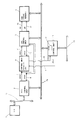
- the designation 1 is used in the drawing for an I/O unit, and 2 for an associated control unit.
- the I/O unit 1 is a secondary memory unit in the example shown here, although all I/O units which transfer data are possible.
- the control unit 2 is so arranged as to handle the transfer of data between the special interface of the I/O unit 1 and a general interface intended for connection to a bus 14, where direct memory access (DMA) is used for data transfer.
- DMA direct memory access
- the expression interface is used here to denote both the circuit solutions and the rules (protocols) required for data transfer.
- the I/O unit 1 is connected in the example illustrated in the drawing to the control unit 2 with the previously disclosed SCSI interface, although the use of other interfaces is possible.
- the designation 3 is used for a control unit for a system bus 13, and 4 for a directly addressable memory.
- the control unit 3 is so arranged as to handle the transfer of data between the system bus 13 and the local bus 14, where DMA can be used for the transfer of data.
- the control unit 3 includes a First-In-First-Out (FIFO) memory 3' for the equalization of the transfer rates between the system bus 13 and the local bus 14.
- FIFO First-In-First-Out
- the interface used for the system bus 13 is of the EISA (Extended Industry System Architecture) type, although control units for buses with other interfaces can be used.
- the memory 4 is connected via the bus 14 and is used here as a cache, although other applications are also possible.
- a control unit for multi-channel DMA is designated in the drawing as 5, and 6 is used to designate a control unit so arranged as to permit the transfer of data between the control unit 2 and the control unit 3.
- the embodiment illustrated in the drawing makes use of three channels, each of which has a DREQ n signal, namely on lines 7, 9 and 11 for DREQ 0 , DREQ 1 and DREQ 2 , in order to indicate that the control unit connected to the signal is ready to transfer data, as well as a DACK n signal, namely on lines 8, 10 and 12 for DACK 0 , DACK 1 and DACK 2 , which is activated by the DMA control unit 5 when transfer can take place.
- the control unit 5 uses write and read signals, WR and RD, intended for the local memory 4.
- the transfer of data between the control unit 2 of the I/O unit 1 and the control unit 3 of the system bus 13 is achieved by activating the DREQ 2 signal 11 connected to the DMA control unit 5 only when the DREQ 0 and DREQ 1 signals are active at the same time.
- the two DACK signals, DACK 0 and DACK 2 are activated in the same way when the DMA control unit 5 activates the DACK 2 signal.
- the possibility of transferring data between two DMA units, each of which is capable of transferring data only to and from a single memory, is thus achieved by using the DMA control unit 5 for bus arbitration and causing the control unit 6 to synchronize the DREQ signals from the two control units 2 and 3 in such a way that the transfer of data only takes place when both units are ready.
- a dedicated DMA channel is used for this purpose.
- the control unit 6 will terminate the transfer of data in those cases in which a local memory is not involved.
- the invention also includes other applications with a DMA control unit and DMA slaves used in conjunction with a control unit for a system bus. These then have the effect of changing the control in such a way that transfer takes place directly or indirectly between the slaves. The DMA control unit and the slaves involved are thus "tricked” into believing that normal DMA transfer is taking place.
- control unit 6 may be constructed in many different ways within the scope of the invention in order to operate in the manner described.
Landscapes
- Engineering & Computer Science (AREA)
- Theoretical Computer Science (AREA)
- Physics & Mathematics (AREA)
- General Engineering & Computer Science (AREA)
- General Physics & Mathematics (AREA)
- Bus Control (AREA)
- Multi Processors (AREA)
- Information Transfer Systems (AREA)
Claims (3)
- Agencement pour le transfert de données entre des unités d'émission de données et de réception de données (1) connectées à un bus de données commun (15), en conjonction avec lesquelles l'agencement comprend une mémoire directement adressable (4) et une unité pour un accès mémoire direct (5) agencées de manière à commander le transfert de données entre les unités d'émission de données et de réception de données (1) mentionnées ci-avant, caractérisé en ce qu'une unité de commande (6) est connectée aux unités d'émission de données et de réception de données (1) ainsi qu'à l'unité d'accès direct mémoire ou DMA (5) mentionnées ci-avant et est agencée de telle sorte que, en conjonction avec le transfert de données depuis une unité d'émission de données jusqu'à une unité de réception de données, elle ait pour effet que le transfert de données inclue également le transfert simultané de données jusqu'à la mémoire directement adressable (4).
- Agencement selon la revendication 1, caractérisé en ce que l'unité de commande (6) est agencée de manière à synchroniser le signal de requête de données ou DREQ et le signal d'accusé de réception de données ou DACK provenant des esclaves alloués aux unités de données et à la mémoire directement adressable (4) de telle sorte que le transfert de données se produise seulement lorsque l'unité de réception de données et la mémoire directement adressable (4) sont toutes deux prêtes pour que celui-ci s'effectue.
- Agencement selon la revendication 2, caractérisé en ce que l'unité de commande (6) est connectée d'une part aux connexions DREQ et DACK des unités d'émission de données et d'autre part à l'unité de DMA via un agencement supplémentaire constitué par des connexions DREQ-DACK disponibles classiquement sur l'unité de commande de DMA (5) et est agencée de manière à activer le signal DREQ sur la connexion supplémentaire de l'unité de commande de DMA (5) lorsque les signaux DREQ des unités de transfert de données sont tous actifs et de manière à activer les signaux DACK des unités de transfert de données lorsque l'unité de commande de DMA a activé la connexion supplémentaire.
Applications Claiming Priority (3)
| Application Number | Priority Date | Filing Date | Title |
|---|---|---|---|
| SE9103450A SE9103450L (sv) | 1991-11-21 | 1991-11-21 | Anordning foer oeverfoering av data mellan datasaendande och datamottagande enheter anslutna till en gemensam databuss. |
| SE9103450 | 1991-11-21 | ||
| PCT/SE1992/000783 WO1993010499A1 (fr) | 1991-11-21 | 1992-11-13 | Configuration concernant le transfert de donnees |
Publications (2)
| Publication Number | Publication Date |
|---|---|
| EP0568678A1 EP0568678A1 (fr) | 1993-11-10 |
| EP0568678B1 true EP0568678B1 (fr) | 1998-06-10 |
Family
ID=20384396
Family Applications (1)
| Application Number | Title | Priority Date | Filing Date |
|---|---|---|---|
| EP92924081A Expired - Lifetime EP0568678B1 (fr) | 1991-11-21 | 1992-11-13 | Configuration concernant le transfert de donnees |
Country Status (5)
| Country | Link |
|---|---|
| EP (1) | EP0568678B1 (fr) |
| DE (1) | DE69225883T2 (fr) |
| FI (1) | FI103078B1 (fr) |
| SE (1) | SE9103450L (fr) |
| WO (1) | WO1993010499A1 (fr) |
Families Citing this family (1)
| Publication number | Priority date | Publication date | Assignee | Title |
|---|---|---|---|---|
| KR100708096B1 (ko) * | 2000-07-21 | 2007-04-16 | 삼성전자주식회사 | 버스 시스템 및 그 실행 순서 조정방법 |
Family Cites Families (4)
| Publication number | Priority date | Publication date | Assignee | Title |
|---|---|---|---|---|
| US4782439A (en) * | 1987-02-17 | 1988-11-01 | Intel Corporation | Direct memory access system for microcontroller |
| JPH0233645A (ja) * | 1988-07-22 | 1990-02-02 | Mitsubishi Electric Corp | コンピュータ |
| JPH02226454A (ja) * | 1989-01-13 | 1990-09-10 | Internatl Business Mach Corp <Ibm> | コンピユータ・システムおよびそのデータ転送方法 |
| JPH077955B2 (ja) * | 1989-05-13 | 1995-01-30 | 株式会社東芝 | データ通信制御装置 |
-
1991
- 1991-11-21 SE SE9103450A patent/SE9103450L/ not_active IP Right Cessation
-
1992
- 1992-11-13 EP EP92924081A patent/EP0568678B1/fr not_active Expired - Lifetime
- 1992-11-13 DE DE69225883T patent/DE69225883T2/de not_active Expired - Fee Related
- 1992-11-13 WO PCT/SE1992/000783 patent/WO1993010499A1/fr not_active Ceased
-
1993
- 1993-07-21 FI FI933288A patent/FI103078B1/fi active
Also Published As
| Publication number | Publication date |
|---|---|
| DE69225883D1 (de) | 1998-07-16 |
| SE468570B (sv) | 1993-02-08 |
| FI933288A7 (fi) | 1993-07-21 |
| FI103078B (fi) | 1999-04-15 |
| DE69225883T2 (de) | 1998-10-08 |
| WO1993010499A1 (fr) | 1993-05-27 |
| SE9103450L (sv) | 1993-02-08 |
| SE9103450D0 (sv) | 1991-11-21 |
| FI103078B1 (fi) | 1999-04-15 |
| EP0568678A1 (fr) | 1993-11-10 |
| FI933288A0 (fi) | 1993-07-21 |
Similar Documents
| Publication | Publication Date | Title |
|---|---|---|
| EP1646925B1 (fr) | Appareil et procede d'acces direct en memoire dans un systeme de memoire basee sur un concentrateur | |
| US4860244A (en) | Buffer system for input/output portion of digital data processing system | |
| JP3598321B2 (ja) | 異なる周波数で動作するバス間でやりとりされるバッファリングデータ | |
| US5274795A (en) | Peripheral I/O bus and programmable bus interface for computer data acquisition | |
| MY109414A (en) | Bus interface logic for computer system having dual bus architecture | |
| US6892266B2 (en) | Multicore DSP device having coupled subsystem memory buses for global DMA access | |
| CA2007737C (fr) | Operations de transfert de donnees entre deux bus asynchrones | |
| US5717875A (en) | Computing device having semi-dedicated high speed bus | |
| JPH09160866A (ja) | バス・インタフェース論理システム及び同期方法 | |
| US4878173A (en) | Controller burst multiplexor channel interface | |
| EP0568678B1 (fr) | Configuration concernant le transfert de donnees | |
| JPH08314854A (ja) | データ転送システムおよびこれに関連する装置 | |
| EP0192578A3 (fr) | Système à bus multiple comprenant un microprocesseur ayant des interfaces et des antémémoires séparées d'instructions et de données | |
| US6609179B1 (en) | Method and apparatus for controlling memory access | |
| US5003461A (en) | Cluster controller memory arbiter | |
| JPH09223103A (ja) | 情報処理システム | |
| EP0439594B1 (fr) | Appareil pour connecter un bus de processeur principal connecte a un processeur principal a un bus peripherique connecte a plusieurs appareils perpheriques | |
| JPH0553902A (ja) | メモリ制御回路 | |
| JP2574821B2 (ja) | ダイレクトメモリアクセス・コントローラ | |
| JPS6217879Y2 (fr) | ||
| JP2682789B2 (ja) | コンピュータ入出力キャッシュ・システム | |
| JPH02211571A (ja) | 情報処理装置 | |
| KR960032662A (ko) | 동기/비동기 버스 접속장치 | |
| JPH07244633A (ja) | インタフェース装置 | |
| KR950020095A (ko) | 데이타 전송능력을 개선한 디.엠.에이(dma) 컨트롤러 |
Legal Events
| Date | Code | Title | Description |
|---|---|---|---|
| PUAI | Public reference made under article 153(3) epc to a published international application that has entered the european phase |
Free format text: ORIGINAL CODE: 0009012 |
|
| 17P | Request for examination filed |
Effective date: 19930707 |
|
| AK | Designated contracting states |
Kind code of ref document: A1 Designated state(s): DE GB |
|
| GRAG | Despatch of communication of intention to grant |
Free format text: ORIGINAL CODE: EPIDOS AGRA |
|
| 17Q | First examination report despatched |
Effective date: 19970623 |
|
| GRAG | Despatch of communication of intention to grant |
Free format text: ORIGINAL CODE: EPIDOS AGRA |
|
| GRAH | Despatch of communication of intention to grant a patent |
Free format text: ORIGINAL CODE: EPIDOS IGRA |
|
| RAP1 | Party data changed (applicant data changed or rights of an application transferred) |
Owner name: ICL SYSTEMS AKTIEBOLAG |
|
| GRAH | Despatch of communication of intention to grant a patent |
Free format text: ORIGINAL CODE: EPIDOS IGRA |
|
| GRAA | (expected) grant |
Free format text: ORIGINAL CODE: 0009210 |
|
| AK | Designated contracting states |
Kind code of ref document: B1 Designated state(s): DE GB |
|
| REF | Corresponds to: |
Ref document number: 69225883 Country of ref document: DE Date of ref document: 19980716 |
|
| PLBE | No opposition filed within time limit |
Free format text: ORIGINAL CODE: 0009261 |
|
| STAA | Information on the status of an ep patent application or granted ep patent |
Free format text: STATUS: NO OPPOSITION FILED WITHIN TIME LIMIT |
|
| 26N | No opposition filed | ||
| REG | Reference to a national code |
Ref country code: GB Ref legal event code: IF02 |
|
| PGFP | Annual fee paid to national office [announced via postgrant information from national office to epo] |
Ref country code: GB Payment date: 20031001 Year of fee payment: 12 |
|
| PGFP | Annual fee paid to national office [announced via postgrant information from national office to epo] |
Ref country code: DE Payment date: 20031027 Year of fee payment: 12 |
|
| PG25 | Lapsed in a contracting state [announced via postgrant information from national office to epo] |
Ref country code: GB Free format text: LAPSE BECAUSE OF NON-PAYMENT OF DUE FEES Effective date: 20041113 |
|
| PG25 | Lapsed in a contracting state [announced via postgrant information from national office to epo] |
Ref country code: DE Free format text: LAPSE BECAUSE OF NON-PAYMENT OF DUE FEES Effective date: 20050601 |
|
| GBPC | Gb: european patent ceased through non-payment of renewal fee |
Effective date: 20041113 |