EP0568995A2 - Halbleiteranordnung mit Kontaktpodesten - Google Patents
Halbleiteranordnung mit Kontaktpodesten Download PDFInfo
- Publication number
- EP0568995A2 EP0568995A2 EP93107292A EP93107292A EP0568995A2 EP 0568995 A2 EP0568995 A2 EP 0568995A2 EP 93107292 A EP93107292 A EP 93107292A EP 93107292 A EP93107292 A EP 93107292A EP 0568995 A2 EP0568995 A2 EP 0568995A2
- Authority
- EP
- European Patent Office
- Prior art keywords
- bump
- metal material
- semiconductor chip
- layers
- layer
- Prior art date
- Legal status (The legal status is an assumption and is not a legal conclusion. Google has not performed a legal analysis and makes no representation as to the accuracy of the status listed.)
- Withdrawn
Links
Images


Classifications
-
- H—ELECTRICITY
- H10—SEMICONDUCTOR DEVICES; ELECTRIC SOLID-STATE DEVICES NOT OTHERWISE PROVIDED FOR
- H10W—GENERIC PACKAGES, INTERCONNECTIONS, CONNECTORS OR OTHER CONSTRUCTIONAL DETAILS OF DEVICES COVERED BY CLASS H10
- H10W72/00—Interconnections or connectors in packages
- H10W72/01—Manufacture or treatment
- H10W72/012—Manufacture or treatment of bump connectors, dummy bumps or thermal bumps
-
- H—ELECTRICITY
- H10—SEMICONDUCTOR DEVICES; ELECTRIC SOLID-STATE DEVICES NOT OTHERWISE PROVIDED FOR
- H10W—GENERIC PACKAGES, INTERCONNECTIONS, CONNECTORS OR OTHER CONSTRUCTIONAL DETAILS OF DEVICES COVERED BY CLASS H10
- H10W72/00—Interconnections or connectors in packages
- H10W72/20—Bump connectors, e.g. solder bumps or copper pillars; Dummy bumps; Thermal bumps
-
- H—ELECTRICITY
- H10—SEMICONDUCTOR DEVICES; ELECTRIC SOLID-STATE DEVICES NOT OTHERWISE PROVIDED FOR
- H10W—GENERIC PACKAGES, INTERCONNECTIONS, CONNECTORS OR OTHER CONSTRUCTIONAL DETAILS OF DEVICES COVERED BY CLASS H10
- H10W72/00—Interconnections or connectors in packages
- H10W72/01—Manufacture or treatment
- H10W72/012—Manufacture or treatment of bump connectors, dummy bumps or thermal bumps
- H10W72/01231—Manufacture or treatment of bump connectors, dummy bumps or thermal bumps using blanket deposition
-
- H—ELECTRICITY
- H10—SEMICONDUCTOR DEVICES; ELECTRIC SOLID-STATE DEVICES NOT OTHERWISE PROVIDED FOR
- H10W—GENERIC PACKAGES, INTERCONNECTIONS, CONNECTORS OR OTHER CONSTRUCTIONAL DETAILS OF DEVICES COVERED BY CLASS H10
- H10W72/00—Interconnections or connectors in packages
- H10W72/01—Manufacture or treatment
- H10W72/012—Manufacture or treatment of bump connectors, dummy bumps or thermal bumps
- H10W72/01231—Manufacture or treatment of bump connectors, dummy bumps or thermal bumps using blanket deposition
- H10W72/01233—Manufacture or treatment of bump connectors, dummy bumps or thermal bumps using blanket deposition in liquid form, e.g. spin coating, spray coating or immersion coating
- H10W72/01235—Manufacture or treatment of bump connectors, dummy bumps or thermal bumps using blanket deposition in liquid form, e.g. spin coating, spray coating or immersion coating by plating, e.g. electroless plating or electroplating
-
- H—ELECTRICITY
- H10—SEMICONDUCTOR DEVICES; ELECTRIC SOLID-STATE DEVICES NOT OTHERWISE PROVIDED FOR
- H10W—GENERIC PACKAGES, INTERCONNECTIONS, CONNECTORS OR OTHER CONSTRUCTIONAL DETAILS OF DEVICES COVERED BY CLASS H10
- H10W72/00—Interconnections or connectors in packages
- H10W72/01—Manufacture or treatment
- H10W72/012—Manufacture or treatment of bump connectors, dummy bumps or thermal bumps
- H10W72/01251—Changing the shapes of bumps
-
- H—ELECTRICITY
- H10—SEMICONDUCTOR DEVICES; ELECTRIC SOLID-STATE DEVICES NOT OTHERWISE PROVIDED FOR
- H10W—GENERIC PACKAGES, INTERCONNECTIONS, CONNECTORS OR OTHER CONSTRUCTIONAL DETAILS OF DEVICES COVERED BY CLASS H10
- H10W72/00—Interconnections or connectors in packages
- H10W72/01—Manufacture or treatment
- H10W72/012—Manufacture or treatment of bump connectors, dummy bumps or thermal bumps
- H10W72/01251—Changing the shapes of bumps
- H10W72/01255—Changing the shapes of bumps by using masks
-
- H—ELECTRICITY
- H10—SEMICONDUCTOR DEVICES; ELECTRIC SOLID-STATE DEVICES NOT OTHERWISE PROVIDED FOR
- H10W—GENERIC PACKAGES, INTERCONNECTIONS, CONNECTORS OR OTHER CONSTRUCTIONAL DETAILS OF DEVICES COVERED BY CLASS H10
- H10W72/00—Interconnections or connectors in packages
- H10W72/20—Bump connectors, e.g. solder bumps or copper pillars; Dummy bumps; Thermal bumps
- H10W72/221—Structures or relative sizes
- H10W72/222—Multilayered bumps, e.g. a coating on top and side surfaces of a bump core
-
- H—ELECTRICITY
- H10—SEMICONDUCTOR DEVICES; ELECTRIC SOLID-STATE DEVICES NOT OTHERWISE PROVIDED FOR
- H10W—GENERIC PACKAGES, INTERCONNECTIONS, CONNECTORS OR OTHER CONSTRUCTIONAL DETAILS OF DEVICES COVERED BY CLASS H10
- H10W72/00—Interconnections or connectors in packages
- H10W72/20—Bump connectors, e.g. solder bumps or copper pillars; Dummy bumps; Thermal bumps
- H10W72/221—Structures or relative sizes
- H10W72/222—Multilayered bumps, e.g. a coating on top and side surfaces of a bump core
- H10W72/223—Multilayered bumps, e.g. a coating on top and side surfaces of a bump core characterised by the structure of the outermost layers, e.g. multilayered coatings
-
- H—ELECTRICITY
- H10—SEMICONDUCTOR DEVICES; ELECTRIC SOLID-STATE DEVICES NOT OTHERWISE PROVIDED FOR
- H10W—GENERIC PACKAGES, INTERCONNECTIONS, CONNECTORS OR OTHER CONSTRUCTIONAL DETAILS OF DEVICES COVERED BY CLASS H10
- H10W72/00—Interconnections or connectors in packages
- H10W72/20—Bump connectors, e.g. solder bumps or copper pillars; Dummy bumps; Thermal bumps
- H10W72/231—Shapes
- H10W72/234—Cross-sectional shape, i.e. in side view
-
- H—ELECTRICITY
- H10—SEMICONDUCTOR DEVICES; ELECTRIC SOLID-STATE DEVICES NOT OTHERWISE PROVIDED FOR
- H10W—GENERIC PACKAGES, INTERCONNECTIONS, CONNECTORS OR OTHER CONSTRUCTIONAL DETAILS OF DEVICES COVERED BY CLASS H10
- H10W72/00—Interconnections or connectors in packages
- H10W72/20—Bump connectors, e.g. solder bumps or copper pillars; Dummy bumps; Thermal bumps
- H10W72/251—Materials
- H10W72/252—Materials comprising solid metals or solid metalloids, e.g. PbSn, Ag or Cu
-
- H—ELECTRICITY
- H10—SEMICONDUCTOR DEVICES; ELECTRIC SOLID-STATE DEVICES NOT OTHERWISE PROVIDED FOR
- H10W—GENERIC PACKAGES, INTERCONNECTIONS, CONNECTORS OR OTHER CONSTRUCTIONAL DETAILS OF DEVICES COVERED BY CLASS H10
- H10W72/00—Interconnections or connectors in packages
- H10W72/90—Bond pads, in general
- H10W72/921—Structures or relative sizes of bond pads
- H10W72/923—Bond pads having multiple stacked layers
-
- H—ELECTRICITY
- H10—SEMICONDUCTOR DEVICES; ELECTRIC SOLID-STATE DEVICES NOT OTHERWISE PROVIDED FOR
- H10W—GENERIC PACKAGES, INTERCONNECTIONS, CONNECTORS OR OTHER CONSTRUCTIONAL DETAILS OF DEVICES COVERED BY CLASS H10
- H10W72/00—Interconnections or connectors in packages
- H10W72/90—Bond pads, in general
- H10W72/951—Materials of bond pads
- H10W72/952—Materials of bond pads comprising metals or metalloids, e.g. PbSn, Ag or Cu
Definitions
- the present invention relates to a semiconductor device having bumps for connection between a semiconductor chip and an external electrode.
- the wireless bonding is a method for connecting all pads on a semiconductor chip to external terminals by respectively associated bumps, which includes the flip chip method and the TAB (Tape Automated Bonding) method.
- Fig. 1 is a cross section to show a structure of a conventional semiconductor chip on which a Au (gold) bump is formed.
- the conventional semiconductor chip is formed by depositing a Ti (titanium)-W (tungsten) alloy 32 on an Al (aluminum) pad 31, a Au layer 33 on the Ti-W alloy 32, and a Au bump 34 on the Au layer 33 by electroplating.
- a bump forming process is described for example in Reference "Semiconductor Fabrication Technology Handbook (handoutai-jissou-gijyutsu Handbook), Chapter 2, Section 9, p.128-138, Flip Chip Bonding, Auther. Soga Fusao, Sept., 1986".
- the mounting (packaging) method using the Au-Sn (gold-tin) eutectic method is such that Sn is deposited by plating on a pad on an external electrode and the Au-Sn eutectic alloy reaction is undergone between the pad and an associated Au bump on semiconductor chip, whereby a surface portion of Au bump melts to effect connection therebetween.
- Fig. 2 shows a state of a Au bump in defective contact with an opposing pad.
- Fig. 2 shows an example in which a semiconductor chip 42 is mounted on a wiring substrate 41. Since a bump 44 is not in contact with a Sn plating 47 on a pad 46, no Au-Sn eutectic alloy reaction takes place at the surface of the bump 44, whereby resulting in defective contact therebetween.
- the conventional semiconductor devices had a problem of low yield in mounting of semiconductor chip due to the defective contact. It is an object of the present invention to solve such a problem.
- a bump is formed by alternately building up two types of metal materials capable of making an eutectic alloy.
- a bump-formed semiconductor chip comprises: a semiconductor chip in which semiconductor elements are formed; and a bump electrically connected with a semiconductor element selected from said semiconductor elements; wherein said bump comprises a layer made of a first metal material and a layer made of a second metal material capable of eutectic-reacting with said first metal material.
- a bump-formed wiring member comprises: a wiring member electrically connected with a semiconductor element formed in a semiconductor chip, in which a desired wiring is formed of a conductor; and a bump electrically connected with said wiring; wherein said bump comprises a layer made of a first metal material and a layer made of a second metal material capable of eutectic-reacting with said first metal material.
- a semiconductor device comprises: a semiconductor chip in which semiconductor elements are formed; a bump electrically connected with a semiconductor element selected from said semiconductor elements; and an external electrode electrically connected with said bump; wherein said bump comprises a layer made of a first metal material and a layer made of a second metal material capable of eutectic-reacting with said first metal material.
- the mounting method of semiconductor chip of the present invention there are bumps formed by alternately building up the two types of metal materials capable of forming an eutectic alloy, so that the eutectic alloy reaction takes place at each boundary surface between layers. Melting of each boundary surface between layers may fully soften the entire bump. Then, an external electrode (semiconductor chip) will moderately encroach on a bump with press in bonding, absorbing unevenness of bump height on the semiconductor chip (external electrode) and a deviation in parallel among the semiconductor chip, the external electrode, and the bumps. In other words, a moderate pressure can assure reliable connection of semiconductor chip on the substrate.
- connection is made using the eutectic alloy reaction, whereby the mounting can be carried out with less damage.
- the mounting method of the present invention is not so sensitive to the bump height dispersion, so that the yield in mounting may be improved.
- Fig. 3 is a schematic cross section to show a structure of a semiconductor chip in the present embodiment.
- a Ti-W alloy 12 is formed on an Al pad 11 on a semiconductor chip 10, securing adherence to the Al pad 11 and serving as a barrier metal to prevent the Al pad 11 and a Au contact layer 13 from forming an intermetallic compound in heat during connection therebetween.
- the Au contact layer 13 is formed on the Ti-W alloy 12, which assures superior plating feasibility in plating of upper Au layer 14 thereon and keeping adherence to the Ti-W alloy 12.
- a protective layer 17 such as SiN covers an area except for the Al pad 11 on the semiconductor chip 10.
- Au layers 14 and Sn layers 15 are alternately built up on the Au contact layer 13 by the electroplating method.
- a multilayered bump 16 is composed of the Au layers 14 and the Sn layers 15.
- the uppermost layer in the bump 16a does not always have to be the Sn layer 15, but may be a Au layer 14.
- the uppermost Au layer 14 would melt by the Au-Sn eutectic alloy reaction during mounting, which allows sure connection with a moderate pressure.
- Sn plating should be provided on a tape or electrode pad.
- the electroplating method is used for formation of the Sn layer 15, but the vacuum evaporation method may also be employed for deposition of Sn layer 15 (in thickness of 0.1-2.0 ⁇ m).
- the bump 16 is formed by alternately building up the Au layers and the Sn layers in the present embodiment as described, the Au-Sn eutectic alloy reaction may take place at each boundary surface between layers in mounting. Then, the entire bump 16 may fully soften. Even if a plurality of bumps provided on a semiconductor chip have a slight dispersion of bump height, secure connection may be obtained with a moderate pressure.
- the bumps are formed on the semiconductor chip in the above description, but the bumps may also be formed on an external electrode such as a wiring (circuit) substrate or a tape used in the TAB method.
- Fig. 5 to Fig. 7 show steps of mounting in the flip chip mounting method.
- the Ti-W alloy 12, the Au contact layer 13, and the protective layer 17 as shown in Fig. 3 and Fig. 4 are omitted.
- a wiring substrate 21 has a conductor portion 211 of desired pattern and three wiring side pads 212a,212b,212c connected therewith and made of Au. Also, three bumps 25a, 25b, 25c are formed on pads 221 of a semiconductor chip 22. Each of these bumps 25a-25c is formed by alternately building up three Au layers 23 and three Sn layers 24 (six layers in total). The uppermost layer (as turning the semiconductor chip 22 upside-down, the lowermost layer in Fig.5 to Fig.7.) in each bump 25a-25c is the Sn layer 24.
- the wiring substrate 21 is first placed under the semiconductor chip 22, and the semiconductor chip 22 is located with the bumps 25a-25c face down.
- the semiconductor chip 22 is aligned with the wiring substrate 21 such that the bumps 25a-25c may contact with corresponding wiring side pads 212a-212c, and the semiconductor chip 22 is then pressed.
- Fig. 5 shows a step before the bumps 25a-25c come into contact with the wiring side pads 212a-212c.
- Fig. 6 shows a step at which the bumps 25a and 25c on either end are in contact with the corresponding wiring side pads 212a and 212c but the shorter bump 25b is not in contact with the wiring side pad 212b.
- the Au-Sn eutectic reaction takes place only in the interface portion between the tip of bump and the wiring side pad, and, therefore, this step is the end of process, leaving the bump 25b as defective in contact.
- the Au-Sn eutectic reaction takes place not only in the interface between the bump tip and the wiring side pad but also at each boundary surface between layers in bump (in this case, 6 surfaces in total), fully softening the entire bump in the present invention.
- the bump 25b may be brought into contact with the wiring side pad 212 as shown in Fig. 7.
- Fig. 8 to Fig. 10 show steps of mounting a semiconductor chip on a printed circuit board by the TAB method.
- the Ti-W alloy 12, the Au contact layer 13, and the protective layer 17 as shown in Fig. 3 and Fig. 4 are omitted.
- a lead frame 29 formed in tape has at one end thereof a lead frame side pad 291 made of Au.
- a bump 28 is formed on a pad 271 of a semiconductor chip 27.
- the bump 28 is formed by alternately building up three Au layers 23 and three Sn layers 24 (six layers in total). The uppermost layer in the bump 28 is the Sn layer 24.
- the lead frame 29 is first set above the semiconductor chip 22 with the lead frame side pad 291 face down, and the semiconductor chip 22 is set with the bump 28 face up.
- the lead frame side pad 291 is aligned to contact with the corresponding bump 28, and the lead frame 29 is then pressed.
- Fig. 8 shows a step before the bump 28 comes into contact with the lead frame side pad 291.
- Fig. 9 shows a state in which the bump 28 is in contact with the lead frame side pad 291 and is securely connected therewith by the eutectic reaction. Also, in case that a plurality of bumps are simultaneously bonded in the TAB method, the defective contact of bump may be eliminated in the same manner as described with the process in the flip chip mounting method. In case that the uppermost layer of the bump 28 is a Au layer instead of Sn layer, Sn plating must be preliminarily provided on the lead frame side pad 291.
- the semiconductor chip 27 electrically connected with the lead frame 29 is mounted on a printed circuit board 26.
- the printed circuit board 26 has a conductor portion 261 of desired pattern and a wiring side pad 262 connected therewith. The mounting is made by soldering of the other end of the lead frame 29 onto the wiring side pad 262, ending in the state as shown in Fig. 10.
- bump characteristic in the present invention including the height of bump, materials of the respective layers, the number of the respective layers, and so on.
- the materials used for bump may be any two types of metals capable of undergoing the eutectic reaction. Specifically, in addition to the combination of Au and Sn as described, the following combinations may be listed up as examples of the materials for bump.
- the Au series includes combinations of base constituents such as Au:Si, Au:Ge, Au:In, Au:Sb, Au:Ga, and Au:Pb.
- the Ag series includes combinations of base constituents such as Ag:Cu into which Zn, Ni, and/or Cd are added.
- the In series includes combinations of base constituents such as In:Sn, In:Ag, and In:Pb.
- the height of the entire bump changes depending upon various conditions of semiconductor chip and others (area, the number of bumps bonded, etc.), usually 10-300 ⁇ m.
- the height of bump is not limited to this range.
- the number of layers in bump the more the easier the entire bump softens, but the minimum number is one layer for each of the two types of metals capable of undergoing the eutectic reaction.
- the number of layers must be increased as the height of the entire bump and the dispersion thereof become greater. In case that the height of the entire bump is below 300 pm, 3-30 layers are suitable for each metal, taking into consideration readiness of process in bump formation, preferably 3-10 layers.
- a ratio of thicknesses of two metal layers does not have to be 1:1 (need not be identical to each other), but should rather be determined considering an operation temperature (that is, eutectic temperature) in bonding process.
- an operation temperature that is, eutectic temperature
- Au:Sn Sn has a lower melting point than Au. Therefore, an increase of Sn in ratio increases a melt part in bump at a lower temperature. It is preferable that Au:Sn be set at 5:1 to 10:1 in actual applications.
- Fig. 11 and Fig. 12 show a first bump forming method in which a bump is formed using the electroplating method similar to the technique as described in Reference " ".
- the reference shows a bump made only of Au, and, therefore, the bump of the present embodiment is different from that in the reference in that the bump is multilayered with alternate Au and Sn.
- An Al pad 101 is formed in a desired area on a semiconductor chip 100 in which semiconductor elements are formed, and a protective layer 102 made of SiN is further formed over the area excluding the Al pad 101 on the semiconductor chip 100.
- a Ti-W alloy layer 103 and a Au contact layer 104 are consecutively deposited over the entire area by evaporation.
- a photoresist is then applied over the entire surface, and a window for bump formation is opened by the photolithography process.
- a Au layer 110 is then formed in thickness of 18 ⁇ m by electroplating.
- a Sn layer 120 is next formed in thickness of 2 ⁇ m by electroplating. These formation steps of the Au layer 110 and the Sn layer 120 are consecutively repeated to form a bump with a desired height (Fig. 11).
- the photoresist 105 is removed, and the evaporation layers (Ti-W alloy layer 103 and Au contact layer 104) are removed except underneath the bump by chemical etching (Fig. 12).
- the Au layers 110 and the Sn layers 120 are formed in bump height of 80 ⁇ m.
- the bump height must be about 200 ⁇ m, and, therefore, the Au layers 110 and the Sn layers 120 are to be formed in ten layers each.
- Fig. 13 and Fig. 14 show a second bump forming method, in which the bump is formed with a thicker photoresist to prevent the horizontal mushroom-like extent of plating layer.
- Steps up to the evaporation of the Au contact layer 104 are the same as those in the first bump forming method as described above.
- a photoresist 106 of sheet dry film is provided (in thickness of not less than 30 ⁇ m) in place of liquid photoresist.
- a window for bump formation is opened by the photolithography process, and Au layers 111 and Sn layers 121 are alternately formed by electroplating (Fig. 13).
- the photoresist 106 is removed, and the evaporation layers (Ti-W alloy layer 103 and Au contact layer 104) are removed except underneath the bump by chemical etching (Fig. 14).
- Fig. 15 to Fig. 17 show a third bump forming method, in which a bump is formed by evaporation. Steps up to the window opening for bump formation are the same as those in the first bump forming method as described. After the window opening, Au layers 112 and Sn layers 122 are alternately deposited by the evaporation method. Further, a photoresist 107 is formed on an area under which a bump is to be formed (Fig. 15). Unnecessary portions of the Au layers 112 and the Sn layers 122 are removed with the photoresist 107 serving as a mask (Fig. 16).
- the photoresists 105 and 107 are removed, and the evaporation layers (Ti-W alloy layer 103 and Au contact layer 104) are removed except underneath the bump by chemical etching (Fig. 17).
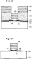
- Fig. 18 and Fig. 19 show a fourth forming method, in which a bump is formed by evaporation and lift-off.
- a photoresist 106 of sheet dry film is used instead of liquid photoresist, in the same manner as in the second bump forming method. Steps up to the window opening for bump formation in the photoresist 106 are the same as those in the second bump forming method.
- Au layers 113 and Sn layers 123 are alternately formed by evaporation (Fig. 18). Then, unnecessary portions of the Au layers 113 and the Sn layers 123 are lifted off by removing the photoresist 106. Further, the evaporation layers (Ti-W alloy layer 103 and Au contact layer 104) are removed except underneath the bump by chemical etching (Fig. 19).
- the evaporation method requires a longer time in formation of layer than the electroplating method, if the thickness is identical. Thus, the evaporation method is inferior in productivity to the electroplating method when it is applied to formation of thicker bump.
- the two method may be suitably combined in formation of bump. For example, in case of forming a bump made of Au (in thickness of 18 ⁇ m):Sn (in thickness of 2 ⁇ m), Au layers may be formed by the electroplating method and Sn layers by the evaporation method.
Landscapes
- Wire Bonding (AREA)
Applications Claiming Priority (2)
| Application Number | Priority Date | Filing Date | Title |
|---|---|---|---|
| JP04113570A JP3141364B2 (ja) | 1992-05-06 | 1992-05-06 | 半導体チップ |
| JP113570/92 | 1992-05-06 |
Publications (2)
| Publication Number | Publication Date |
|---|---|
| EP0568995A2 true EP0568995A2 (de) | 1993-11-10 |
| EP0568995A3 EP0568995A3 (de) | 1993-12-08 |
Family
ID=14615601
Family Applications (1)
| Application Number | Title | Priority Date | Filing Date |
|---|---|---|---|
| EP19930107292 Withdrawn EP0568995A3 (de) | 1992-05-06 | 1993-05-05 | Halbleiteranordnung mit Kontaktpodesten |
Country Status (8)
| Country | Link |
|---|---|
| US (1) | US5461261A (de) |
| EP (1) | EP0568995A3 (de) |
| JP (1) | JP3141364B2 (de) |
| KR (1) | KR930024090A (de) |
| AU (1) | AU663777B2 (de) |
| CA (1) | CA2095058A1 (de) |
| MY (1) | MY131396A (de) |
| TW (1) | TW260825B (de) |
Cited By (3)
| Publication number | Priority date | Publication date | Assignee | Title |
|---|---|---|---|---|
| US5634268A (en) * | 1995-06-07 | 1997-06-03 | International Business Machines Corporation | Method for making direct chip attach circuit card |
| US5796591A (en) * | 1995-06-07 | 1998-08-18 | International Business Machines Corporation | Direct chip attach circuit card |
| EP0887851A3 (de) * | 1997-06-23 | 1999-08-18 | Ford Motor Company | Verfahren zur Bildung von Verbindungen auf elektronischen Modulen |
Families Citing this family (48)
| Publication number | Priority date | Publication date | Assignee | Title |
|---|---|---|---|---|
| US5435482A (en) * | 1994-02-04 | 1995-07-25 | Lsi Logic Corporation | Integrated circuit having a coplanar solder ball contact array |
| AU6761996A (en) * | 1995-07-20 | 1997-02-18 | Dallas Semiconductor Corporation | Method and apparatus for encryption key creation |
| JP3310499B2 (ja) * | 1995-08-01 | 2002-08-05 | 富士通株式会社 | 半導体装置 |
| US5789271A (en) * | 1996-03-18 | 1998-08-04 | Micron Technology, Inc. | Method for fabricating microbump interconnect for bare semiconductor dice |
| US5808360A (en) * | 1996-05-15 | 1998-09-15 | Micron Technology, Inc. | Microbump interconnect for bore semiconductor dice |
| US5912510A (en) * | 1996-05-29 | 1999-06-15 | Motorola, Inc. | Bonding structure for an electronic device |
| US5620611A (en) * | 1996-06-06 | 1997-04-15 | International Business Machines Corporation | Method to improve uniformity and reduce excess undercuts during chemical etching in the manufacture of solder pads |
| WO1998012597A1 (fr) * | 1996-09-20 | 1998-03-26 | Hitachi, Ltd. | Dispositif d'affichage a cristaux liquides, son procede de fabrication et telephone mobile |
| US5841198A (en) * | 1997-04-21 | 1998-11-24 | Lsi Logic Corporation | Ball grid array package employing solid core solder balls |
| US6372624B1 (en) | 1997-08-04 | 2002-04-16 | Micron Technology, Inc. | Method for fabricating solder bumps by wave soldering |
| US6107122A (en) * | 1997-08-04 | 2000-08-22 | Micron Technology, Inc. | Direct die contact (DDC) semiconductor package |
| TW453137B (en) * | 1997-08-25 | 2001-09-01 | Showa Denko Kk | Electrode structure of silicon semiconductor device and the manufacturing method of silicon device using it |
| KR100447895B1 (ko) * | 1997-09-13 | 2004-10-14 | 삼성전자주식회사 | 칩 스케일 패키지 및 그 제조방법 |
| JP4066522B2 (ja) * | 1998-07-22 | 2008-03-26 | イビデン株式会社 | プリント配線板 |
| US6242935B1 (en) | 1999-01-21 | 2001-06-05 | Micron Technology, Inc. | Interconnect for testing semiconductor components and method of fabrication |
| JP3553413B2 (ja) * | 1999-04-26 | 2004-08-11 | 富士通株式会社 | 半導体装置の製造方法 |
| JP4593717B2 (ja) * | 2000-02-23 | 2010-12-08 | 京セラ株式会社 | 回路基板及びそれを用いた回路装置 |
| US6429531B1 (en) * | 2000-04-18 | 2002-08-06 | Motorola, Inc. | Method and apparatus for manufacturing an interconnect structure |
| US6610591B1 (en) | 2000-08-25 | 2003-08-26 | Micron Technology, Inc. | Methods of ball grid array |
| US6348740B1 (en) * | 2000-09-05 | 2002-02-19 | Siliconware Precision Industries Co., Ltd. | Bump structure with dopants |
| DE10063914A1 (de) * | 2000-12-20 | 2002-07-25 | Pac Tech Gmbh | Kontakthöckeraufbau zur Herstellung eines Verbindungsaufbaus zwischen Substratanschlussflächen |
| US20020151164A1 (en) * | 2001-04-12 | 2002-10-17 | Jiang Hunt Hang | Structure and method for depositing solder bumps on a wafer |
| US6902098B2 (en) * | 2001-04-23 | 2005-06-07 | Shipley Company, L.L.C. | Solder pads and method of making a solder pad |
| US6527159B2 (en) * | 2001-07-12 | 2003-03-04 | Intel Corporation | Surface mounting to an irregular surface |
| US7057294B2 (en) * | 2001-07-13 | 2006-06-06 | Rohm Co., Ltd. | Semiconductor device |
| US7547623B2 (en) | 2002-06-25 | 2009-06-16 | Unitive International Limited | Methods of forming lead free solder bumps |
| US7223633B2 (en) * | 2002-11-27 | 2007-05-29 | Intel Corporation | Method for solder crack deflection |
| JP4115306B2 (ja) * | 2003-03-13 | 2008-07-09 | 富士通株式会社 | 半導体装置の製造方法 |
| TWI229436B (en) * | 2003-07-10 | 2005-03-11 | Advanced Semiconductor Eng | Wafer structure and bumping process |
| KR100712534B1 (ko) * | 2005-09-22 | 2007-04-27 | 삼성전자주식회사 | 콘택 저항을 최소화할 수 있는 볼을 갖는 패키지 및 테스트장치, 그리고 그 패키지의 제조 방법 |
| US20070102815A1 (en) * | 2005-11-08 | 2007-05-10 | Kaufmann Matthew V | Bumping process with self-aligned A1-cap and the elimination of 2nd passivation layer |
| WO2007120418A2 (en) * | 2006-03-13 | 2007-10-25 | Nextwire Systems, Inc. | Electronic multilingual numeric and language learning tool |
| JP4219951B2 (ja) * | 2006-10-25 | 2009-02-04 | 新光電気工業株式会社 | はんだボール搭載方法及びはんだボール搭載基板の製造方法 |
| US20090020876A1 (en) * | 2007-07-20 | 2009-01-22 | Hertel Thomas A | High temperature packaging for semiconductor devices |
| US8293587B2 (en) | 2007-10-11 | 2012-10-23 | International Business Machines Corporation | Multilayer pillar for reduced stress interconnect and method of making same |
| US7947592B2 (en) * | 2007-12-14 | 2011-05-24 | Semiconductor Components Industries, Llc | Thick metal interconnect with metal pad caps at selective sites and process for making the same |
| US7994043B1 (en) | 2008-04-24 | 2011-08-09 | Amkor Technology, Inc. | Lead free alloy bump structure and fabrication method |
| JP5535448B2 (ja) | 2008-05-19 | 2014-07-02 | シャープ株式会社 | 半導体装置、半導体装置の実装方法、および半導体装置の実装構造 |
| JP2011138913A (ja) * | 2009-12-28 | 2011-07-14 | Citizen Holdings Co Ltd | 半導体発光素子とその製造方法 |
| TWM397591U (en) * | 2010-04-22 | 2011-02-01 | Mao Bang Electronic Co Ltd | Bumping structure |
| JP5774292B2 (ja) * | 2010-11-04 | 2015-09-09 | セミコンダクター・コンポーネンツ・インダストリーズ・リミテッド・ライアビリティ・カンパニー | 回路装置およびその製造方法 |
| WO2012085724A1 (en) * | 2010-12-21 | 2012-06-28 | Koninklijke Philips Electronics N.V. | Method of fabricating a flip chip electrical coupling, a flip chip electrical coupling, and a device comprising a flip chip electrical coupling |
| US8387854B2 (en) * | 2011-02-25 | 2013-03-05 | Memsic, Inc. | Method for mounting a three-axis MEMS device with precise orientation |
| WO2013147808A1 (en) * | 2012-03-29 | 2013-10-03 | Intel Corporation | Functional material systems and processes for package-level interconnects |
| DE102012216546B4 (de) | 2012-09-17 | 2023-01-19 | Infineon Technologies Ag | Verfahren zum verlöten eines halbleiterchips mit einem träger |
| US20150318254A1 (en) * | 2013-12-17 | 2015-11-05 | Oracle International Corporation | Electroplated solder with eutectic chemical composition |
| US9748196B2 (en) * | 2014-09-15 | 2017-08-29 | Advanced Semiconductor Engineering, Inc. | Semiconductor package structure including die and substrate electrically connected through conductive segments |
| KR102860672B1 (ko) * | 2020-07-30 | 2025-09-17 | 삼성디스플레이 주식회사 | 전자장치 |
Family Cites Families (9)
| Publication number | Priority date | Publication date | Assignee | Title |
|---|---|---|---|---|
| FR1483574A (de) * | 1965-06-24 | 1967-09-06 | ||
| US3436818A (en) * | 1965-12-13 | 1969-04-08 | Ibm | Method of fabricating a bonded joint |
| US3986255A (en) * | 1974-11-29 | 1976-10-19 | Itek Corporation | Process for electrically interconnecting chips with substrates employing gold alloy bumps and magnetic materials therein |
| US3959522A (en) * | 1975-04-30 | 1976-05-25 | Rca Corporation | Method for forming an ohmic contact |
| JPS5839047A (ja) * | 1981-09-02 | 1983-03-07 | Hitachi Ltd | 半導体装置およびその製法 |
| JPS6187396A (ja) * | 1984-10-05 | 1986-05-02 | 株式会社日立製作所 | 電子回路装置とその製造方法 |
| US4875617A (en) * | 1987-01-20 | 1989-10-24 | Citowsky Elya L | Gold-tin eutectic lead bonding method and structure |
| US4922322A (en) * | 1989-02-09 | 1990-05-01 | National Semiconductor Corporation | Bump structure for reflow bonding of IC devices |
| US5197654A (en) * | 1991-11-15 | 1993-03-30 | Avishay Katz | Bonding method using solder composed of multiple alternating gold and tin layers |
-
1992
- 1992-05-06 JP JP04113570A patent/JP3141364B2/ja not_active Expired - Fee Related
-
1993
- 1993-04-28 AU AU38205/93A patent/AU663777B2/en not_active Ceased
- 1993-04-28 CA CA002095058A patent/CA2095058A1/en not_active Abandoned
- 1993-04-30 TW TW082103378A patent/TW260825B/zh active
- 1993-05-03 KR KR1019930007569A patent/KR930024090A/ko not_active Ceased
- 1993-05-03 MY MYPI93000824A patent/MY131396A/en unknown
- 1993-05-05 EP EP19930107292 patent/EP0568995A3/de not_active Withdrawn
-
1994
- 1994-12-19 US US08/358,979 patent/US5461261A/en not_active Expired - Fee Related
Cited By (5)
| Publication number | Priority date | Publication date | Assignee | Title |
|---|---|---|---|---|
| US5634268A (en) * | 1995-06-07 | 1997-06-03 | International Business Machines Corporation | Method for making direct chip attach circuit card |
| US5796591A (en) * | 1995-06-07 | 1998-08-18 | International Business Machines Corporation | Direct chip attach circuit card |
| EP0887851A3 (de) * | 1997-06-23 | 1999-08-18 | Ford Motor Company | Verfahren zur Bildung von Verbindungen auf elektronischen Modulen |
| US6082610A (en) * | 1997-06-23 | 2000-07-04 | Ford Motor Company | Method of forming interconnections on electronic modules |
| US6250541B1 (en) | 1997-06-23 | 2001-06-26 | Visteon Global Technologies, Inc. | Method of forming interconnections on electronic modules |
Also Published As
| Publication number | Publication date |
|---|---|
| CA2095058A1 (en) | 1993-11-07 |
| JP3141364B2 (ja) | 2001-03-05 |
| US5461261A (en) | 1995-10-24 |
| EP0568995A3 (de) | 1993-12-08 |
| JPH05315338A (ja) | 1993-11-26 |
| TW260825B (de) | 1995-10-21 |
| MY131396A (en) | 2007-08-30 |
| AU3820593A (en) | 1993-11-11 |
| AU663777B2 (en) | 1995-10-19 |
| KR930024090A (ko) | 1993-12-21 |
Similar Documents
| Publication | Publication Date | Title |
|---|---|---|
| US5461261A (en) | Semiconductor device with bumps | |
| US5518957A (en) | Method for making a thin profile semiconductor package | |
| US4494688A (en) | Method of connecting metal leads with electrodes of semiconductor device and metal lead therefore | |
| US5008997A (en) | Gold/tin eutectic bonding for tape automated bonding process | |
| US5698465A (en) | Process for manufacturing an interconnect bump for flip-chip integrated circuit including integral standoff and hourglass shaped solder coating | |
| KR100265616B1 (ko) | 도전성 폴리머 및 유전체를 이용한 플립칩 | |
| KR100555706B1 (ko) | 미세 솔더볼 구현을 위한 ubm 및 이를 이용한 플립칩패키지 방법 | |
| US20050116344A1 (en) | Microelectronic element having trace formed after bond layer | |
| JP3015436B2 (ja) | 半導体装置およびその接続方法 | |
| JPH07201864A (ja) | 突起電極形成方法 | |
| US20040209452A1 (en) | Solder terminal and fabricating method thereof | |
| JP2001148401A (ja) | 半導体装置およびその製造方法 | |
| US5053851A (en) | Metal bump for a thermal compression bond and method for making same | |
| US5396702A (en) | Method for forming solder bumps on a substrate using an electrodeposition technique | |
| EP0540519B1 (de) | Verfahren zur Herstellung einer Thermokompressionsverbindung | |
| JPH0195539A (ja) | 半導体装置及びその製造方法 | |
| EP0359228A2 (de) | Eutektische Verbindung mit Gold/Zinn für die automatische Bandmontage-Technik | |
| JP3267422B2 (ja) | バンプ転写体および半導体集積回路装置の製造方法 | |
| JPH05166812A (ja) | 半導体素子 | |
| KR960002770B1 (ko) | 탭(tab) 패키지의 테이프 본딩방법 | |
| JP3967999B2 (ja) | フリップチップ型icの製造方法 | |
| JP2822506B2 (ja) | 半導体装置の製造方法 | |
| JP3351878B2 (ja) | 半導体装置およびその製造方法 | |
| KR100523298B1 (ko) | 금 범프가 형성된 반도체 칩과 그 제조방법 | |
| JP2001237261A (ja) | 半導体装置およびその製造方法 |
Legal Events
| Date | Code | Title | Description |
|---|---|---|---|
| PUAI | Public reference made under article 153(3) epc to a published international application that has entered the european phase |
Free format text: ORIGINAL CODE: 0009012 |
|
| PUAL | Search report despatched |
Free format text: ORIGINAL CODE: 0009013 |
|
| AK | Designated contracting states |
Kind code of ref document: A2 Designated state(s): CH DE FR GB IT LI NL |
|
| AK | Designated contracting states |
Kind code of ref document: A3 Designated state(s): CH DE FR GB IT LI NL |
|
| 17P | Request for examination filed |
Effective date: 19940608 |
|
| 17Q | First examination report despatched |
Effective date: 19950620 |
|
| 18W | Application withdrawn |
Withdrawal date: 19960620 |