EP0569219B1 - Circuit de protection d'entrée pouvant supporter une tension élevée - Google Patents
Circuit de protection d'entrée pouvant supporter une tension élevée Download PDFInfo
- Publication number
- EP0569219B1 EP0569219B1 EP93303468A EP93303468A EP0569219B1 EP 0569219 B1 EP0569219 B1 EP 0569219B1 EP 93303468 A EP93303468 A EP 93303468A EP 93303468 A EP93303468 A EP 93303468A EP 0569219 B1 EP0569219 B1 EP 0569219B1
- Authority
- EP
- European Patent Office
- Prior art keywords
- region
- esd
- circuit
- protection device
- breakdown
- Prior art date
- Legal status (The legal status is an assumption and is not a legal conclusion. Google has not performed a legal analysis and makes no representation as to the accuracy of the status listed.)
- Expired - Lifetime
Links
Images





Classifications
-
- H—ELECTRICITY
- H10—SEMICONDUCTOR DEVICES; ELECTRIC SOLID-STATE DEVICES NOT OTHERWISE PROVIDED FOR
- H10D—INORGANIC ELECTRIC SEMICONDUCTOR DEVICES
- H10D89/00—Aspects of integrated devices not covered by groups H10D84/00 - H10D88/00
- H10D89/60—Integrated devices comprising arrangements for electrical or thermal protection, e.g. protection circuits against electrostatic discharge [ESD]
- H10D89/601—Integrated devices comprising arrangements for electrical or thermal protection, e.g. protection circuits against electrostatic discharge [ESD] for devices having insulated gate electrodes, e.g. for IGFETs or IGBTs
- H10D89/711—Integrated devices comprising arrangements for electrical or thermal protection, e.g. protection circuits against electrostatic discharge [ESD] for devices having insulated gate electrodes, e.g. for IGFETs or IGBTs using bipolar transistors as protective elements
-
- H—ELECTRICITY
- H10—SEMICONDUCTOR DEVICES; ELECTRIC SOLID-STATE DEVICES NOT OTHERWISE PROVIDED FOR
- H10D—INORGANIC ELECTRIC SEMICONDUCTOR DEVICES
- H10D89/00—Aspects of integrated devices not covered by groups H10D84/00 - H10D88/00
- H10D89/60—Integrated devices comprising arrangements for electrical or thermal protection, e.g. protection circuits against electrostatic discharge [ESD]
- H10D89/601—Integrated devices comprising arrangements for electrical or thermal protection, e.g. protection circuits against electrostatic discharge [ESD] for devices having insulated gate electrodes, e.g. for IGFETs or IGBTs
- H10D89/611—Integrated devices comprising arrangements for electrical or thermal protection, e.g. protection circuits against electrostatic discharge [ESD] for devices having insulated gate electrodes, e.g. for IGFETs or IGBTs using diodes as protective elements
Definitions
- the present invention relates generally to electrostatic discharge (ESD) protection of integrated circuits. More particularly, the invention relates to ESD protection of high voltage power (>25V) input terminals, especially for applications where power devices are used in conjunction with printing elements to form a customer replacable unit such as a printhead or print cartridge which will be handled in a wide variety of environments that are hostile to semiconductor components.
- ESD electrostatic discharge
- MOS integrated circuits Numerous conventional systems are known for ESD protection of semiconductor and MOS devices.
- the inputs of MOS integrated circuits are capacitors whose two electrodes are the MOS transistor device channel and the gate electrode material, usually polysilicon.
- the two capacitor electrodes are separated by silicon dioxide, which is usually grown on the device channel by high temperature oxidation processes.
- the MOS transistors use a thin silicon dioxide gate insulator to achieve high performance, and this thin oxide is susceptable to catastrophic, irreversable breakdown if the voltage across the dielectric is raised above 20 to 100 volts, depending on device fabrication details.
- Such circuits use monolithically integrated protective transistors built into the semiconductor circuit to protect the gates of the devices. These protective transistors are arranged to allow a high voltage static discharge transient to pass to ground prior to reaching the protected circuit.
- U.S. Patent 4,990,984 to discloses a conventional protective transistor ESD protection device for an integrated circuit.
- Such systems have at least three disadvantages which prevent them from being applied as protection of high voltage power input terminals.
- the conventional protective transistor for the circuit has only a small current carrying capacity, so that ESD surges which are encountered in the office environment will overwhelm the protective transistor, allowing a part of the ESD surge to reach the protected circuit or causing failure of the ESD protection circuit itself.
- conventional protective transistors are designed to protect logic input terminals, which have a low current signal input voltage of 5V. Accordingly, these protective transistors are designed to break down at 15 to 25V.
- Advanced VLSI technologies utilize reduced gate dielectric thickness and CMOS fabrication, so the industry trend is to reduce the voltage at which ESD input protection structures breakdown, since the gate dielectric becomes more susceptable to breakdown as it becomes thinner.
- US Patent No. 5 027 252 describes use of a three stage protection circuit.
- the first stage is a punch through device under field oxide, and is connected directly to the input pad.
- the second stage is isolated from the first stage by a current limiting diffused resistor and is a thick oxide device with its gate tied to the input pad.
- the diffused resistor is situated between the gate connection and the drain, and the device source is tied to ground.
- a second diffused resistor is then followed by the third stage, where a conventional n-channel device with its gate and source tied to ground is used to discharge any remaining voltage to ground.
- US Patent No. 4 616 243 describes techniques for protecting p-well CMOS logic inputs.
- a polysilicon current limiting resistor is connected to the input pad and is followed by an n-channel device which is placed in a p-well that is specifically tailored to breakdown before normal p-well transistors.
- the breakdown voltage is lowered by raising the doping level of the protective transistor p-well, diffusing the p-well to a shallower depth, or adding diffused features which reduce p-well breakdown by other methods.
- Document EP-A-0 058 557 discloses a lateral bipolar transistor for protecting an element of a semiconductor device.
- a semiconductor device according to the present invention is defined in claim 1.
- a semiconductor or MOS integrated circuit 10 comprises a high voltage input terminal 12 and input impedance 16, a number of semiconductor circuit elements 14 comprising the protected circuit and an electrostatic discharge (ESD) protection device 18.
- the input impedance 16 represents the various parasitic resistances arising from the input terminal and the input line, and, in the illustrated arrangement, has a resistance less than 10 ⁇ .
- the load 14a is a 150 ⁇ resistive heating element for a thermal ink jet printer printhead.
- the heaters 14a of the individual power MOS drivers 14b must be heated the same amount independent of whether a particular resistor 14a is being used alone or in conjunction with other resistors 14a. That is, it is important that the same heat energy, within a few percent, be delivered whether one or more heaters are simultaneously activated by control circuitry 19.
- the input impedance 16 must be less than 100 ⁇ , is desirably less than 10 ⁇ and is preferably less than 1 ⁇ .
- the circuit elements 14 operate at a voltage of 20V-100V and a current of 200mA-800mA. In printers providing densities up to 1200 spi, the circuit elements will operate at a lower current. For example it is anticipated that a 800-1200 spi printhead will operate on a current on the order of 50 mA. While it is recognized that other printers may not require the high current sourcing of the illustrated arrangement, it is obvious that the resistance 16 of the input 12 in a power circuit must be kept low.
- a thermal ink jet printer may contain many blocks of circuit elements 14, such as 32 blocks (for 128 jet printheads) or 48 blocks (for 192 jet printheads). A 384 jet printhead (96 blocks) which is able to fire up to 8 circuit elements 14 at once has also been built.
- the circuit elements 14 are connected in parallel between the parasitic input impedance 16 and ground, while the impedance 16 is connected in serial to input pad 12.
- the load 14a is connected in series with the drain of the power MOS driver 14b.
- the source of the power MOS driver 14b is connected to ground and the gate of power MOS driver 14b is connected to a control circuit 19 (not shown in detail).
- the ESD protection device 18 is also connected in parallel with the circuit elements 14 between the impedance 16 and ground.
- the ESD protection device 18 is a thick oxide transistor, as shown in Figures 6a and 6b.
- Electrostatic discharge (ESD) events occur when a person's body becomes highly charged and the individual then touches a grounded object and discharges. The discharge is very similar to the discharge of a capacitor. It can be anticipated that ESD events depend on many variables. Electrical engineers have studied ESD events and developed a model called the "Human Body Model (HBM)". An HBM ESD event is simulated by discharging a 100 pF capacitor through 1.5 k ⁇ resistance, and the time constant for discharge is about 150 nsec. Therefore, the ESD event is of short duration and high current flow. ESD testing of a device would typically consist of charging up the capacitor to increasingly higher voltages and discharging it through the device until the device fails.
- HBM Human Body Model
- Figures 2 and 3 show a plan and sectional view of the layout of one power MOS driver of a 300 spot per inch (SPI) thermal ink jet printhead.
- SPI spot per inch
- the aluminum drain contacts 34 must be made close to the drift region 25, as shown in Figures 2 and 3.
- the space in between a via 34 and the gate 26 is only 7 ⁇ m. In higher resolution printheads (e.g. 400 spi), the spacing will be even closer.
- FIGS 4 and 5 illustrate the breakdown mechanism.
- the breakdown mechanism is the same for both the power MOS drivers 14b and the ESD protection device 18.
- avalanche breakdown of the drain junction caused by the ESD event will supply the initial carriers (i.e. turning the device "ON") necessary to start the feedback loop.
- the drain 24, which is connected to the high voltage input pad 12 by metallization layer 30 is biased at a high voltage.
- the high voltage at the drain 24 depletes carriers in the drift region 25 and in the substrate region 20.
- the depleted boundary regions 45 are also shown.
- a high electric field exists at the left edge of the drift layer 25. When the field exceeds the breakdown strength of silicon, avalanche breakdown begins. Electron-hole pairs are created at the edge of the drift region and electrons enter the drain 24. Once in the substrate, the holes 43 are drawn to ground, creating a substrate hole current. Due to the resistance R sub of the substrate, a potential appears between the substrate region 20 in the vicinity of the device and ground.
- the bipolar feedback loop is suppressed in the power MOS circuit by locating the input protection device 18 in parallel with the power MOS drivers 14b.
- the protection device 18 is designed to have a lower breakdown point so that avalanche breakdown in the power MOS drivers is prevented.
- the ESD protection device 18 is also designed to survive the bipolar feedback loop by placing the high voltage input pad metallization via contact 30 further away from the avalanche region to prevent eutectic alloying and junction spiking from occurring.
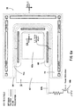
- the structure of the protection device 18 is shown in Figures 6a-6c.
- the input terminal 62 of the metallization layer has an input contact pad 62a and a lead region 62b connected to the protected circuit 14.
- Region 64 of the metallization layer connects the three independent lobes of the protection circuit 18 to ground.
- Each lobe of the protection circuit 18 is an independent protection device for protecting multiple blocks of 2 or more circuits 14.
- Figure 6b shows a top view of the input terminal 12 and the protection device of one lobe of the protection circuit 18.
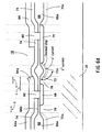
- Figures 6c and 6d show the sectional view through one lobe on the line(6b,c - 6b,c) of Figure 6a.
- the substrate region 20 (which is a p - region) has a first n + diffusion region 68 connected to the input terminal pad 62a and a second n + diffusion region 70 connected to the ground metallization layer 64 through vias 80. Lying atop the first and second n + diffusion regions 68 and 70 is an oxide layer 66 (including regions 66a and 66b) and a phosphorosilicate glass (PSG) layer 74.
- the first n + diffusion region 68 is electrically isolated from the second n + diffusion region 70 by field oxide 66a and a channel stop 72 of the substrate 20.
- the diffusion region 70 is shown located in the p - region 20 of the substrate, it could be located in the substrate adjacent that region.
- the oxide layer 66 has the first or source-drain reoxidized regions 66b when lying over the first or second n + diffusion regions 68 and 70 and has the second or field oxide regions 66a extending over the substrate 20.
- the regions 66a of oxide layer 66 are located to the left of first n + diffusion region 68, to the right of the second n + diffusion region 70, and in the region 72 lying between the first and second n + diffusion regions 68 and 70.
- a p region 72 is formed in the substrate region 20 as a channel stop region. Such p channel stop regions 72 may also be formed in the substrate below the left and right thickened field oxide regions 66a.
- the central p channel stop region 72 is separated from the first n + diffusion region 68 by a first n - drift region 78.
- the leftmost p channel stop region 72 may be separated from the first n + diffusion region 68 by a second n - drift region 76.
- the second n + diffusion region 70 abuts the central p channel stop region 72 and the rightmost p channel stop region 72.
- the spacing between the aluminum contact 80 and avalanche breakdown region 78a is shown in Figure 6c as dimension "z”.
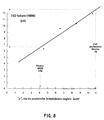
- Figure 8 shows the ESD hardness of the ESD protection device as a function of "z”. Power MOS ESD hardness is also shown in Figure 8.
- the close via spacing in the power MOS device results in low ESD hardness, while the large via spacing in the ESD protection device provides high ESD hardness. Because the ESD protection device takes up small area, there is little penalty for the via spacing used, while there would be a large penalty paid for such a large spacing in the power MOS devices.
- the power MOS device(s) 14b to be protected have drains 24 made of n + diffusion. High drain breakdown is achieved by spacing the drain 24 away from the polysilicon gate electrodes 26 by a lightly doped drift region 25 ( Figure 4). The drift region 25 abuts the silicon region below the gate electrode 26, where a p-type threshold adjustment implant 36 is located.
- the source 22 is also constructed of n + diffusion and surrounds the drain region 24.
- the power MOS device described here would be a "pull down" device and the source is therefore always at ground. Alternative configurations would have the same drain structure but alternative source configurations.
- An offset gate lateral power MOS is used here for illustration, but the concept is more generally applicable to a variety of power device designs such as DMOS, bipolar, and others.
- the objective is to assure that the power MOS devices 14b breakdown at a higher voltage than the ESD protection circuitry 18. This is assured by using the same n - doping for the drift layer 25 of the power MOS device 14b as for the drift layer 78 of the ESD protection circuitry 18, by making the drift layer 25 of the power MOS driver 14b have a lateral dimension equal to or greater than the lateral dimension of the drift layer 78 of the ESD circuitry 18 and by abutting the drift layer 78 of the ESD protection device 18 to a more heavily doped p-type region than the threshold adjustment doping 36 which is present in the power MOS devices.
- the drift region 78 of the ESD protection device 18 abuts the channel stop p-type region 72 and also the threshold adjustment implant 36 in the power MOS driver 14b.
- the general power MOS driver circuit is in particular a power NMOS driver circuit which is suitable for integration with an NMOS logic process architecture.
- the n - drift region 78 of the protection device 18 has a masked n-type depletion implant added to it.
- the depletion implant converts logic devices to be normally "ON” instead of normally “OFF”.
- the effective drift layer becomes more highly n-type in the ESD protection circuit 18 only. This assures that the ESD protection device 18 will breakdown prior to the power MOS drivers 14b.
- the depletion implant extends across the entire lateral dimension of the n - drift region 78 between the first n + diffusion region 68 and the central p + channel stop region 72.
- the depletion implant extends only partially across the via dimension of the n - drift region 78. In this case, depletion doping is added to the half of the drift layer 78 adjacent to diffusion 68.
- a lower resistance n - drift region is substituted in the ESD circuit 18 for the original n - drift region 78 while the relatively higher original resistance of the drift layer 25 of the power MOS devices 14b is retained.
- this fourth arrangement has the disadvantage of requiring an additional mask and processing step, which are necessary to create the lower resistance drift region.
- the well-technology described in the previously-mentioned US Patents 5 027 252 and 4 616 243 can be incorporated into the ESD protective circuit 18 when CMOS-type power MOS drivers are used.
- that arrangement suffers the same problems as the fourth arrangement, in that additional masks and processing steps will be required. Additional masks and processing steps will undesirably raise both the cost and the complexity of chip manufacturing.
- the lateral dimension of the n - drift region 78 of the ESD protective circuit 18, represented by the dimension X of Figure 6c, is made shorter than the lateral dimension of the n - drift region 25 of the power MOS driver, as shown in Figure 3.
- the n - drift layer 25 is several microns long. Therefore it is simple to make the n - drift region 78 of the protective circuit 18 several microns shorter.
- the n - drift layer 25 can be made 4-5 ⁇ m long, while the n - drift layer 78 of the protection device 18 can be made 3-4 ⁇ m.
- the drift layer is made shorter, the potential gradient through it is higher and the avalanche breakdown point is lower.
- the drift region 78 may have a sheet resistance of at least 1 kohm/square and width of at least two microns and may surround the diffusion region 68 (which may be degenerately doped) at least laterally.
- the metallization layer 62a which connects the first n + diffusion region 68 to the input pad 62 is extended to lie over the n - drift layer 78.
- this extension or field plate 64a can be easily added during the normal metallization step by simply altering the metallization layer mask.
- the field plate 64a can be attached to the ground connection layer 64 instead of the input terminal pad 62a.
- the drift layer will accumulate and cause breakdown at a lower voltage. Accumulation of the drift layer will cause the ESD protection device to breakdown at a lower voltage, but has the undesirable effect of attracting hot electrons toward the SiO 2 interface.
- An alternative and preferable configuration is to repel hot electrons by attaching the field plate 64a to ground metallization 64.
- the n - drift region 78 is buried so that the peak n-type dopant concentration is below the surface level of the substrate 20. The effect of that is to move the avalanche breakdown point 78a away from the silicon-field oxide interface.
- a ninth arrangement which is in accordance with the present invention uses a p + doping of the substrate to form the second diffusion region 70 instead of the n + doping used in the previous arrangements.
- a Zener diode is formed rather than a bipolar transistor.
- the bipolar transistor follows the curve 102 as voltage rises above the breakdown point V A .
- the curve 102 is called a "snapback" curve and indicates that after breakdown, the bipolar transistor arrangements (1-8) described above have a reduced voltage drop across the protection circuit as current increases.
- a disadvantage of bipolar action is that the resultant ESD circuit may exhibit thermal runaway in a small region before other segments can conduct.
- Zener diode of the ninth arrangement has an identical breakdown point V A , it follows the curve 104.
- the Zener diode form experiences no snapback, it is able to provide a more robust protection circuit than the bipolar transistor arrangements for the case where parasitic bipolar gain is nonuniform.
- the Zener diode requires another processing step to provide the p + doping.
- the p + layer may be available as a substrate contact.
- the ninth arrangement can be combined with any of the arrangements 3 to 8 described above to further improve the performance of the ninth arrangement.
Landscapes
- Semiconductor Integrated Circuits (AREA)
- Metal-Oxide And Bipolar Metal-Oxide Semiconductor Integrated Circuits (AREA)
Claims (1)
- Dispositif à semi-conducteur comprenant un dispositif de protection contre la décharge électrostatique (ESD) (18) comportant une diode de Zener destinée à protéger un dispositif à semi-conducteur de puissance (14b) qui est formé sur un substrat de silicium (20) et qui est connecté à une borne à tension élevée (12), dans lequel le dispositif de protection contre l'ESD est également formé sur le substrat et est connecté à la borne en parallèle au dispositif à semi-conducteur de puissance; et dans lequel la tension de claquage du dispositif à semi conducteur de puissance est plus grande que la tension de claquage du dispositif de protection contre l'ESD, et la résistance à l'ESD du dispositif de protection contre l'ESD est plus grande que la résistance à l'ESD du dispositif à semi-conducteur de puissance, ledit dispositif de protection contre l'ESD comprenant :au moins une région légèrement dopée p (20) dans le substrat;une région de diffusion n- (68) prévue dans la région légèrement dopée p et connectée à la borne à tension élevée;une région de diffusion p+ (70) prévue dans la région légèrement dopée p ou dans le substrat au voisinage de la région légèrement dopée p et connectée à la terre;une région d'arrêt de canal modérément dopée p (72) prévue dans la région légèrement dopée p entre la région de diffusion n+ et la région de diffusion p+ et au voisinage de la région de diffusion p-;au moins une région d'impulsion n- (78) située entre la région d'arrêt de canal modérément dopée p et la région de diffusion n+.
Applications Claiming Priority (2)
| Application Number | Priority Date | Filing Date | Title |
|---|---|---|---|
| US879626 | 1992-05-06 | ||
| US07/879,626 US5371395A (en) | 1992-05-06 | 1992-05-06 | High voltage input pad protection circuitry |
Publications (3)
| Publication Number | Publication Date |
|---|---|
| EP0569219A2 EP0569219A2 (fr) | 1993-11-10 |
| EP0569219A3 EP0569219A3 (en) | 1995-11-08 |
| EP0569219B1 true EP0569219B1 (fr) | 1998-06-10 |
Family
ID=25374531
Family Applications (1)
| Application Number | Title | Priority Date | Filing Date |
|---|---|---|---|
| EP93303468A Expired - Lifetime EP0569219B1 (fr) | 1992-05-06 | 1993-05-04 | Circuit de protection d'entrée pouvant supporter une tension élevée |
Country Status (4)
| Country | Link |
|---|---|
| US (1) | US5371395A (fr) |
| EP (1) | EP0569219B1 (fr) |
| JP (1) | JPH0621343A (fr) |
| DE (1) | DE69319021T2 (fr) |
Families Citing this family (30)
| Publication number | Priority date | Publication date | Assignee | Title |
|---|---|---|---|---|
| US5428498A (en) * | 1992-09-28 | 1995-06-27 | Xerox Corporation | Office environment level electrostatic discharge protection |
| KR0166101B1 (ko) * | 1993-10-21 | 1999-01-15 | 김주용 | 정전방전 보호회로의 트랜지스터 및 그 제조방법 |
| DE4423591C2 (de) * | 1994-07-06 | 1996-08-29 | Itt Ind Gmbh Deutsche | Schutzstruktur für integrierte Schaltungen |
| US5733794A (en) * | 1995-02-06 | 1998-03-31 | Motorola, Inc. | Process for forming a semiconductor device with ESD protection |
| US5701024A (en) * | 1995-10-05 | 1997-12-23 | Cypress Semiconductor Corp. | Electrostatic discharge (ESD) protection structure for high voltage pins |
| KR100402672B1 (ko) * | 1995-10-31 | 2004-06-04 | 텍사스 인스트루먼츠 인코포레이티드 | CMOS/BiCMOS기술에서ESD방지를위한집적화된횡형구조 |
| JP2787908B2 (ja) * | 1995-12-25 | 1998-08-20 | 日本電気株式会社 | 半導体装置の製造方法 |
| JPH09248912A (ja) * | 1996-01-11 | 1997-09-22 | Canon Inc | インクジェットヘッド及びヘッド用基体、インクジェットカートリッジ、並びにインクジェット装置 |
| US6071768A (en) * | 1996-05-17 | 2000-06-06 | Texas Instruments Incorporated | Method of making an efficient NPN turn-on in a high voltage DENMOS transistor for ESD protection |
| TW320772B (en) * | 1996-09-23 | 1997-11-21 | United Microelectronics Corp | Protection component and production method for low voltage static discharge |
| US5910873A (en) * | 1997-02-19 | 1999-06-08 | National Semiconductor Corporation | Field oxide transistor based feedback circuit for electrical overstress protection |
| US6501136B1 (en) * | 1997-09-16 | 2002-12-31 | Winbond Electronics Corporation | High-speed MOSFET structure for ESD protection |
| US5936284A (en) | 1997-11-03 | 1999-08-10 | Sgs-Thomson Microelectronics S.R.L. | Electrostatic discharge protection circuit and transistor |
| US5960290A (en) * | 1998-10-29 | 1999-09-28 | United Microelectronics Corp. | Method for fabricating a protection circuit of electrostatic discharge on a field device |
| US6114194A (en) * | 1998-11-17 | 2000-09-05 | United Microelectronics Corp. | Method for fabricating a field device transistor |
| US6487507B1 (en) * | 1999-10-15 | 2002-11-26 | Micro Motion, Inc. | Remote signal conditioner for a Coriolis flowmeter |
| JP2002370363A (ja) * | 2001-06-15 | 2002-12-24 | Canon Inc | インクジェット記録ヘッド用基板、インクジェット記録ヘッド、インクジェット記録装置 |
| JP2003072076A (ja) * | 2001-08-31 | 2003-03-12 | Canon Inc | 記録ヘッド及びその記録ヘッドを用いた記録装置 |
| JP4125153B2 (ja) * | 2002-02-20 | 2008-07-30 | キヤノン株式会社 | 半導体装置及びそれを用いた液体吐出装置 |
| US7021748B2 (en) * | 2002-07-19 | 2006-04-04 | Canon Kabushiki Kaisha | Ink jet head substrate, ink jet head using the substrate, and ink jet print apparatus |
| US6940131B2 (en) * | 2003-06-30 | 2005-09-06 | Texas Instruments Incorporated | MOS ESD CDM clamp with integral substrate injection guardring and method for fabrication |
| US7267430B2 (en) * | 2005-03-29 | 2007-09-11 | Lexmark International, Inc. | Heater chip for inkjet printhead with electrostatic discharge protection |
| US7450431B1 (en) * | 2005-08-24 | 2008-11-11 | Xilinx, Inc. | PMOS three-terminal non-volatile memory element and method of programming |
| US7420842B1 (en) | 2005-08-24 | 2008-09-02 | Xilinx, Inc. | Method of programming a three-terminal non-volatile memory element using source-drain bias |
| US7687797B1 (en) | 2005-08-24 | 2010-03-30 | Xilinx, Inc. | Three-terminal non-volatile memory element with hybrid gate dielectric |
| US7544968B1 (en) | 2005-08-24 | 2009-06-09 | Xilinx, Inc. | Non-volatile memory cell with charge storage element and method of programming |
| US7361966B2 (en) * | 2006-02-13 | 2008-04-22 | Lexmark International, Inc. | Actuator chip for inkjet printhead with electrostatic discharge protection |
| US8488288B2 (en) * | 2008-06-27 | 2013-07-16 | National Instruments Corporation | Input protection method with variable tripping threshold and low parasitic elements |
| JP5121976B2 (ja) * | 2011-05-27 | 2013-01-16 | 株式会社東芝 | 半導体装置 |
| JP5537683B2 (ja) * | 2013-01-21 | 2014-07-02 | 株式会社東芝 | 半導体装置 |
Family Cites Families (18)
| Publication number | Priority date | Publication date | Assignee | Title |
|---|---|---|---|---|
| JPS5650527A (en) * | 1979-09-29 | 1981-05-07 | Fujitsu Ltd | Semiconductor integrated circuit device |
| US4602267A (en) * | 1981-02-17 | 1986-07-22 | Fujitsu Limited | Protection element for semiconductor device |
| JPS60767A (ja) * | 1983-06-17 | 1985-01-05 | Hitachi Ltd | 半導体装置 |
| EP0157389B1 (fr) * | 1984-03-31 | 1991-06-26 | Kabushiki Kaisha Toshiba | Dispositif de protection pour un transistor MOS |
| JPS6153761A (ja) * | 1984-08-24 | 1986-03-17 | Hitachi Ltd | 半導体装置 |
| US4803536A (en) * | 1986-10-24 | 1989-02-07 | Xerox Corporation | Electrostatic discharge protection network for large area transducer arrays |
| US4987465A (en) * | 1987-01-29 | 1991-01-22 | Advanced Micro Devices, Inc. | Electro-static discharge protection device for CMOS integrated circuit inputs |
| JPS63248170A (ja) * | 1987-04-02 | 1988-10-14 | Nec Corp | 半導体装置 |
| JPH0712060B2 (ja) * | 1987-07-02 | 1995-02-08 | 日本電気株式会社 | 相補型mosデバイスの入力保護装置 |
| FR2623018B1 (fr) * | 1987-11-06 | 1990-02-09 | Thomson Semiconducteurs | Circuit integre protege contre les decharges electrostatiques avec seuil de protection variable |
| JPH01140757A (ja) * | 1987-11-27 | 1989-06-01 | Nec Corp | 半導体入力保護装置 |
| US4947192A (en) * | 1988-03-07 | 1990-08-07 | Xerox Corporation | Monolithic silicon integrated circuit chip for a thermal ink jet printer |
| JPH0227738A (ja) * | 1988-07-15 | 1990-01-30 | Seiko Epson Corp | 半導体装置 |
| US5055896A (en) * | 1988-12-15 | 1991-10-08 | Siliconix Incorporated | Self-aligned LDD lateral DMOS transistor with high-voltage interconnect capability |
| JP2626229B2 (ja) * | 1989-10-12 | 1997-07-02 | 日本電気株式会社 | 半導体入力保護装置 |
| JPH0734477B2 (ja) * | 1990-05-28 | 1995-04-12 | 株式会社東芝 | 半導体装置の製造方法 |
| EP0473129B1 (fr) * | 1990-08-29 | 1998-05-13 | Texas Instruments Incorporated | Cellule de mémoire rémanente asymétrique, réseaux et procédé pour la fabrication |
| US5075250A (en) * | 1991-01-02 | 1991-12-24 | Xerox Corporation | Method of fabricating a monolithic integrated circuit chip for a thermal ink jet printhead |
-
1992
- 1992-05-06 US US07/879,626 patent/US5371395A/en not_active Expired - Fee Related
-
1993
- 1993-04-28 JP JP5101701A patent/JPH0621343A/ja active Pending
- 1993-05-04 EP EP93303468A patent/EP0569219B1/fr not_active Expired - Lifetime
- 1993-05-04 DE DE69319021T patent/DE69319021T2/de not_active Expired - Fee Related
Also Published As
| Publication number | Publication date |
|---|---|
| EP0569219A3 (en) | 1995-11-08 |
| DE69319021T2 (de) | 1998-12-10 |
| DE69319021D1 (de) | 1998-07-16 |
| US5371395A (en) | 1994-12-06 |
| EP0569219A2 (fr) | 1993-11-10 |
| JPH0621343A (ja) | 1994-01-28 |
Similar Documents
| Publication | Publication Date | Title |
|---|---|---|
| US5371395A (en) | High voltage input pad protection circuitry | |
| US5072273A (en) | Low trigger voltage SCR protection device and structure | |
| JP2699654B2 (ja) | トリガ電圧を低減したscr保護構造および回路 | |
| EP0535536B1 (fr) | Etage d'isolation contrôlé par appauvrissement | |
| US5907462A (en) | Gate coupled SCR for ESD protection circuits | |
| US5404041A (en) | Source contact placement for efficient ESD/EOS protection in grounded substrate MOS integrated circuit | |
| JP3484081B2 (ja) | 半導体集積回路及び保護素子 | |
| US20080044955A1 (en) | Electrostatic discharge protection device for digital circuits and for applications with input/output bipolar voltage much higher than the core circuit power supply | |
| US20070284666A1 (en) | Local ESD Protection for Low-Capicitance Applications | |
| US6521952B1 (en) | Method of forming a silicon controlled rectifier devices in SOI CMOS process for on-chip ESD protection | |
| US7728349B2 (en) | Low capacitance SCR with trigger element | |
| US8143673B1 (en) | Circuit with electrostatic discharge protection | |
| EP0590859B1 (fr) | Protection contre des décharges électrostatiques à un niveau d'environnement de bureau | |
| US5493133A (en) | PNP punchthrough-assisted protection device for special applications in CMOS technologies | |
| US7838937B1 (en) | Circuits providing ESD protection to high voltage laterally diffused metal oxide semiconductor (LDMOS) transistors | |
| US6900969B2 (en) | ESD protection with uniform substrate bias | |
| US6347026B1 (en) | Input and power protection circuit implemented in a complementary metal oxide semiconductor process using salicides | |
| US6455898B1 (en) | Electrostatic discharge input protection for reducing input resistance | |
| KR100380768B1 (ko) | 반도체 장치 | |
| JP2505652B2 (ja) | 低トリガ電圧scr保護装置及び構造 | |
| EP0793272A2 (fr) | Structure de protection comprenant une diode pour un plat de contact | |
| EP0606667A1 (fr) | Dispositif semi-conducteur avec un circuit intégré pourvu de moyens de protection contre des surtensions | |
| EP0568341A2 (fr) | Structure de protection contre des décharges électrostatiques | |
| KR100189036B1 (ko) | 반도체 디바이스 | |
| EP0688054A2 (fr) | Protection contre des décharges électrostatiques pour un dispositif semi-conducteur de circuit intégré |
Legal Events
| Date | Code | Title | Description |
|---|---|---|---|
| PUAI | Public reference made under article 153(3) epc to a published international application that has entered the european phase |
Free format text: ORIGINAL CODE: 0009012 |
|
| AK | Designated contracting states |
Kind code of ref document: A2 Designated state(s): DE FR GB |
|
| PUAL | Search report despatched |
Free format text: ORIGINAL CODE: 0009013 |
|
| AK | Designated contracting states |
Kind code of ref document: A3 Designated state(s): DE FR GB |
|
| 17P | Request for examination filed |
Effective date: 19960508 |
|
| 17Q | First examination report despatched |
Effective date: 19961004 |
|
| GRAG | Despatch of communication of intention to grant |
Free format text: ORIGINAL CODE: EPIDOS AGRA |
|
| GRAG | Despatch of communication of intention to grant |
Free format text: ORIGINAL CODE: EPIDOS AGRA |
|
| GRAH | Despatch of communication of intention to grant a patent |
Free format text: ORIGINAL CODE: EPIDOS IGRA |
|
| GRAH | Despatch of communication of intention to grant a patent |
Free format text: ORIGINAL CODE: EPIDOS IGRA |
|
| GRAA | (expected) grant |
Free format text: ORIGINAL CODE: 0009210 |
|
| AK | Designated contracting states |
Kind code of ref document: B1 Designated state(s): DE FR GB |
|
| REF | Corresponds to: |
Ref document number: 69319021 Country of ref document: DE Date of ref document: 19980716 |
|
| ET | Fr: translation filed | ||
| PLBE | No opposition filed within time limit |
Free format text: ORIGINAL CODE: 0009261 |
|
| STAA | Information on the status of an ep patent application or granted ep patent |
Free format text: STATUS: NO OPPOSITION FILED WITHIN TIME LIMIT |
|
| 26N | No opposition filed | ||
| REG | Reference to a national code |
Ref country code: GB Ref legal event code: IF02 |
|
| PGFP | Annual fee paid to national office [announced via postgrant information from national office to epo] |
Ref country code: GB Payment date: 20020501 Year of fee payment: 10 |
|
| PGFP | Annual fee paid to national office [announced via postgrant information from national office to epo] |
Ref country code: FR Payment date: 20020508 Year of fee payment: 10 Ref country code: DE Payment date: 20020508 Year of fee payment: 10 |
|
| PG25 | Lapsed in a contracting state [announced via postgrant information from national office to epo] |
Ref country code: GB Free format text: LAPSE BECAUSE OF NON-PAYMENT OF DUE FEES Effective date: 20030504 |
|
| PG25 | Lapsed in a contracting state [announced via postgrant information from national office to epo] |
Ref country code: DE Free format text: LAPSE BECAUSE OF NON-PAYMENT OF DUE FEES Effective date: 20031202 |
|
| GBPC | Gb: european patent ceased through non-payment of renewal fee |
Effective date: 20030504 |
|
| PG25 | Lapsed in a contracting state [announced via postgrant information from national office to epo] |
Ref country code: FR Free format text: LAPSE BECAUSE OF NON-PAYMENT OF DUE FEES Effective date: 20040130 |
|
| REG | Reference to a national code |
Ref country code: FR Ref legal event code: ST |