EP0575757A1 - Procédé et dispositif pour découper une plaquette semi-conductrice - Google Patents
Procédé et dispositif pour découper une plaquette semi-conductrice Download PDFInfo
- Publication number
- EP0575757A1 EP0575757A1 EP93108304A EP93108304A EP0575757A1 EP 0575757 A1 EP0575757 A1 EP 0575757A1 EP 93108304 A EP93108304 A EP 93108304A EP 93108304 A EP93108304 A EP 93108304A EP 0575757 A1 EP0575757 A1 EP 0575757A1
- Authority
- EP
- European Patent Office
- Prior art keywords
- wafer
- cutting edge
- displacement
- cutting
- edge
- Prior art date
- Legal status (The legal status is an assumption and is not a legal conclusion. Google has not performed a legal analysis and makes no representation as to the accuracy of the status listed.)
- Granted
Links
Images




Classifications
-
- H—ELECTRICITY
- H10—SEMICONDUCTOR DEVICES; ELECTRIC SOLID-STATE DEVICES NOT OTHERWISE PROVIDED FOR
- H10P—GENERIC PROCESSES OR APPARATUS FOR THE MANUFACTURE OR TREATMENT OF DEVICES COVERED BY CLASS H10
- H10P52/00—Grinding, lapping or polishing of wafers, substrates or parts of devices
-
- B—PERFORMING OPERATIONS; TRANSPORTING
- B23—MACHINE TOOLS; METAL-WORKING NOT OTHERWISE PROVIDED FOR
- B23D—PLANING; SLOTTING; SHEARING; BROACHING; SAWING; FILING; SCRAPING; LIKE OPERATIONS FOR WORKING METAL BY REMOVING MATERIAL, NOT OTHERWISE PROVIDED FOR
- B23D59/00—Accessories specially designed for sawing machines or sawing devices
- B23D59/001—Measuring or control devices, e.g. for automatic control of work feed pressure on band saw blade
- B23D59/002—Measuring or control devices, e.g. for automatic control of work feed pressure on band saw blade for the position of the saw blade
-
- B—PERFORMING OPERATIONS; TRANSPORTING
- B28—WORKING CEMENT, CLAY, OR STONE
- B28D—WORKING STONE OR STONE-LIKE MATERIALS
- B28D5/00—Fine working of gems, jewels, crystals, e.g. of semiconductor material; apparatus or devices therefor
- B28D5/02—Fine working of gems, jewels, crystals, e.g. of semiconductor material; apparatus or devices therefor by rotary tools, e.g. drills
- B28D5/022—Fine working of gems, jewels, crystals, e.g. of semiconductor material; apparatus or devices therefor by rotary tools, e.g. drills by cutting with discs or wheels
- B28D5/028—Fine working of gems, jewels, crystals, e.g. of semiconductor material; apparatus or devices therefor by rotary tools, e.g. drills by cutting with discs or wheels with a ring blade having an inside cutting edge
Definitions
- the present invention relates to a method of slicing a semiconductor wafer and an apparatus therefor, in particular, to a method of slicing a semiconductor wafer and an apparatus therefor in which a bowl-shaped wafer can be manufactured.
- a blade tip portion of an inner peripheral cutting edge or an outer peripheral cutting edge is composed of fine diamond grains.
- the blade tip is abraded partially by use.
- a cutting curve in either direction is drawn according to this partial abrasion. For instance, when a cutting blade is curved upward by the abrasion, a shape of a wafer is curved more upward according to a increase in a cutting resistance as cutting progresses, so that the curving displacement of the upper side becomes the maximum because the cutting resistance is made maximum at the maximum cutting length.
- the cutting resistance becomes small according as a cutting length gradually becomes small, so that the curving displacement becomes also small gradually.
- the above-mentioned method of slicing has a problem in that a wafer is worked in a shape curved upward or downward.
- a curving control of the wafer is executed to eliminate the problem. That is, the blade displacement is detected with a sensor, and the curving control is performed in such a manner that the blade displacement at the position of this sensor becomes zero by moving the air pad.
- an air pad is moved in a manner that the displacement of the center part at the cutting position of a semiconductor material becomes zero, and the semiconductor material is cut.
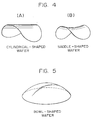
- the conventional method of slicing has a disadvantage in that a wafer is formed like a part of cylinder or a saddle as shown in Figs. 4 (A) and (B) because the air pad is controlled in such a manner that the blade displacement of a sensor position or a center position becomes zero.
- the wafer forming a part of cylinder and the saddle-shaped wafer are disadvantageous for the postprocessing of the wafer unlike a bowl-shaped wafer shown in Fig. 5.
- the present invention aims at proposing a method of slicing a semiconductor wafer and an apparatus therefor which can manufacture a bowl-shaped wafer.
- a method of slicing a semiconductor wafer and an apparatus therefor wherein a cutting edge is mounted on a rotatable spindle, a semiconductor material is pressed on the cutting edge, either one of the cutting edge and the semiconductor material is moved in a manner to relatively approach the other, and the semiconductor material is cut into thin pieces
- said method comprising the steps of sensing an axial displacement of the cutting edge by a sensor and cutting the wafer while correcting the displacement by an air pad, characterized in that said air pad is controlled in such a manner that the displacement value of the cutting edge at the circumferential edge of the wafer to be cut becomes zero from the positional relationship between said sensor and said air pad to the circumferential edge to be cut out of the semiconductor material, this edge is changeable during the cutting.
- the movement value of the air pad is decided in such a manner that the blade displacement at the circumferential edge of the wafer to be cut becomes zero from the positional relationship between said sensor and said air pad to the changeable cutting position, so that the displacement of the wafer to be cut at each cutting position of semiconductor material can be adjusted to zero. Therefore, a bowl-shaped wafer can be manufactured.
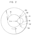
- a chuck body 12 is firmly secured to the upper end portion of a spindle 10, while the lower end portion of a spindle 10 is connected to a rotor(which is not shown).
- the spindle 10 and the chuck body 12 can be rotated by means of the motor.
- the outer peripheral edge of a doughnut-shaped blade 14 is stretched up onto the chuck body 12.
- the blade 14 includes an inner peripheral cutting edge 16 along the inner peripheral cutting edge portion thereof.
- the inner peripheral cutting edge 16 is made up fine diamond grains and the like.
- the blade 14 is also arranged such that the tension of the outer peripheral edge thereof can be adjusted by a well known stretching mechanism (not shown) provided in the chuck body 12.
- the upper end portion of a semiconductor ingot 18 is secured fixedly to a work support base 21.
- the ingot 18 can be moved in a cutting/feeding direction (that is, a direction of X-X) with a cutting/feeding mechanism 22 and the work support base 21 can be moved in the work indexing direction (that is, a direction of Z-Z) with a work indexing mechanism 24.
- the cutting/feeding mechanism 22 and the work dividing mechanism 24 are driven by instruction signals from a control unit 26.
- a pair of air pads 30, 30 of a non-contact type and a pair of blade sensors 32, 32 are arranged on the upper surface of the blade 14.
- the displacement of the blade 14 is detected with the blade sensors 32, 32 and can be corrected with the air pads 30, 30.
- the blade sensor 32, 32 are connected with the control unit 26.
- the control unit 26 controls a air pressure control device 36 to move the air pads 30, 30.
- a slicing method according to the present invention can be effected in the following manner.
- the ingot 18 is moved in the direction of X aiming at the inner peripheral cutting edge 16, and then cutting is started.
- the relationship between the cutting resistance, the cutting length and the ingot delivery speed are that the cutting resistance increases in proportion as the cutting length becomes longer and as the ingot delivery speed becomes higher.
- the cutting resistance increases, it is in the nature that the displacement of the blade 14 becomes larger and the blade 14 becomes to curve easily.
- the sensor 32 detects the displacement of the blade 14 as shown in Fig. 3
- the air pad 30 is controlled in curve according to the curve (c) shown in Fig.
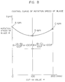
- a curve in Fig. 8 indicates the relationship between the blade rotation speed R and the cut-in value e, the maximum value of the cut-in value is 200mm.
- Curves in Fig. 9 indicate the relationship between the work delivery speed and the cut-in value to make the displacement on the center line of the wafer an oval when the outer peripheral displacement of the wafer is controlled to be zero.
- a curve (a) indicates a case that the blade rotation speed is not controlled.
- a curve (b) indicates a case that the blade rotation speed is controlled.
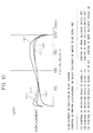
- curves Fig. 10 indicate the relationship between the blade displacement and the cut-in value at the position of the sensor when the outer peripheral displacement of the wafer is controlled to be zero.
- a curve (c) indicates a case that both the blade rotation speed and the work delivery speed are not controlled.
- a curve (d) indicates a case that the blade rotation speed is controlled but the work delivery speed is not controlled.
- a curve (e) indicates a case that the work delivery speed is controlled regardless whether the blade rotation speed is controlled or not.
- the curving control is performed by the blade rotation speed control shown in Fig. 8, the work delivery speed control indicated by the curve (b) in Fig. 9 and the blade displacement control indicated by the curve (e) in Fig. 10.
- the curving control is performed by the work delivery speed control indicated by the curve (a) in Fig. 9 and the blade displacement control indicated by the curve (e) in Fig. 10.
- the curving control is performed by the blade rotation speed control shown in Fig. 8 and the blade displacement control indicated by the curve (d) in Fig.10.
- the displacement of the blade 14 is detected with a pair of sensors 32, 32 to perform the curving control.
- the blade displacement of the center of the cutting position is detected with a eddy-current sensor provided at the center of the cutting position. Then, the displacement of the wafer circumferential edge may be found by the blade displacement.
- the cutting blade displacement value at the circumferential edge of the semiconductor material to be cut is obtained by the cutting blade displacement value detected with the sensor and the air pads control the displacement at the circumferential edge of the semiconductor wafer, so that a bowl-shaped wafer can be manufactured.
Landscapes
- Engineering & Computer Science (AREA)
- Mechanical Engineering (AREA)
- Processing Of Stones Or Stones Resemblance Materials (AREA)
- Mechanical Treatment Of Semiconductor (AREA)
- Finish Polishing, Edge Sharpening, And Grinding By Specific Grinding Devices (AREA)
Applications Claiming Priority (2)
| Application Number | Priority Date | Filing Date | Title |
|---|---|---|---|
| JP132678/92 | 1992-05-25 | ||
| JP4132678A JPH05318460A (ja) | 1992-05-25 | 1992-05-25 | 半導体ウエハのスライシング方法 |
Publications (2)
| Publication Number | Publication Date |
|---|---|
| EP0575757A1 true EP0575757A1 (fr) | 1993-12-29 |
| EP0575757B1 EP0575757B1 (fr) | 1997-03-19 |
Family
ID=15086954
Family Applications (1)
| Application Number | Title | Priority Date | Filing Date |
|---|---|---|---|
| EP93108304A Expired - Lifetime EP0575757B1 (fr) | 1992-05-25 | 1993-05-21 | Procédé et dispositif pour découper une plaquette semi-conductrice |
Country Status (5)
| Country | Link |
|---|---|
| US (1) | US5458526A (fr) |
| EP (1) | EP0575757B1 (fr) |
| JP (1) | JPH05318460A (fr) |
| KR (1) | KR0185235B1 (fr) |
| DE (1) | DE69308937T2 (fr) |
Families Citing this family (8)
| Publication number | Priority date | Publication date | Assignee | Title |
|---|---|---|---|---|
| US5628673A (en) * | 1993-11-26 | 1997-05-13 | Seiko Seiki Kabushiki Kaisha | Dicing machine with non-contact setup function |
| US5632666A (en) * | 1994-10-28 | 1997-05-27 | Memc Electronic Materials, Inc. | Method and apparatus for automated quality control in wafer slicing |
| JP3195504B2 (ja) * | 1994-11-24 | 2001-08-06 | トーヨーエイテック株式会社 | スライシング装置のブレード変位検出装置 |
| JP2943673B2 (ja) * | 1995-10-31 | 1999-08-30 | 日本電気株式会社 | 半導体基板の製造装置及び製造方法 |
| DE19607695A1 (de) * | 1996-02-29 | 1997-09-04 | Wacker Siltronic Halbleitermat | Verfahren zur Herstellung von Halbleiterscheiben |
| CN101804670B (zh) * | 2003-10-16 | 2012-06-27 | 日立金属株式会社 | 工件切断装置和工件切断方法 |
| CN102229010A (zh) * | 2011-04-01 | 2011-11-02 | 浙江恒成硬质合金有限公司 | 切片机 |
| CN117656272A (zh) * | 2021-11-01 | 2024-03-08 | 青岛高测科技股份有限公司 | 硅棒切割系统的切割装置及硅棒切割系统 |
Citations (4)
| Publication number | Priority date | Publication date | Assignee | Title |
|---|---|---|---|---|
| DE3908153A1 (de) * | 1988-03-11 | 1989-09-21 | Mitsubishi Metal Corp | Innenwirksame schneidscheibe |
| EP0456223A1 (fr) * | 1990-05-10 | 1991-11-13 | Tokyo Seimitsu Co.,Ltd. | Machine pour couper et procédé de découpage avec celle-ci |
| EP0476952A2 (fr) * | 1990-09-14 | 1992-03-25 | Shin-Etsu Handotai Company Limited | Procédé et appareil pour la division en tranches d'un lingot monocristallin au moyen d'une scie annulaire |
| EP0513437A1 (fr) * | 1991-05-17 | 1992-11-19 | Mitsubishi Materials Corporation | Dispositif pour ajuster la position de lame de coupe sur des machines à couper |
Family Cites Families (10)
| Publication number | Priority date | Publication date | Assignee | Title |
|---|---|---|---|---|
| US3327696A (en) * | 1964-10-09 | 1967-06-27 | Howard Aiken Ind | Saw stabilizing means and method |
| JPS6147644A (ja) * | 1984-08-13 | 1986-03-08 | Hitachi Ltd | スライサ−用ブレ−ドのそり制御方法 |
| JPH0818329B2 (ja) * | 1986-11-26 | 1996-02-28 | 三菱マテリアル株式会社 | ウエ−ハの切断不良検出方法 |
| US5025593A (en) * | 1988-01-18 | 1991-06-25 | Mazda Motor Corporation | Slicing machine and control method thereof |
| JPH01206006A (ja) * | 1988-02-12 | 1989-08-18 | Mazda Motor Corp | スライシングマシン切刃変位検出装置 |
| JP2598314B2 (ja) * | 1988-11-14 | 1997-04-09 | 住友シチックス株式会社 | 硬脆材料の切断装置 |
| JPH03221410A (ja) * | 1990-01-29 | 1991-09-30 | Tokyo Seimitsu Co Ltd | 柱状体材料の切断方法 |
| JPH03221411A (ja) * | 1990-01-29 | 1991-09-30 | Tokyo Seimitsu Co Ltd | 柱状体材料の切断方法 |
| JPH0439005A (ja) * | 1990-06-06 | 1992-02-10 | Tsusho Sangyo Kenkyusha:Kk | スライシングマシン及びその制御方法 |
| JPH04122609A (ja) * | 1990-09-13 | 1992-04-23 | Tsusho Sangyo Kenkyusha:Kk | スライシングマシン及びその制御方法 |
-
1992
- 1992-05-25 JP JP4132678A patent/JPH05318460A/ja active Pending
-
1993
- 1993-05-21 EP EP93108304A patent/EP0575757B1/fr not_active Expired - Lifetime
- 1993-05-21 DE DE69308937T patent/DE69308937T2/de not_active Expired - Fee Related
- 1993-05-24 US US08/065,755 patent/US5458526A/en not_active Expired - Fee Related
- 1993-05-25 KR KR1019930009105A patent/KR0185235B1/ko not_active Expired - Fee Related
Patent Citations (4)
| Publication number | Priority date | Publication date | Assignee | Title |
|---|---|---|---|---|
| DE3908153A1 (de) * | 1988-03-11 | 1989-09-21 | Mitsubishi Metal Corp | Innenwirksame schneidscheibe |
| EP0456223A1 (fr) * | 1990-05-10 | 1991-11-13 | Tokyo Seimitsu Co.,Ltd. | Machine pour couper et procédé de découpage avec celle-ci |
| EP0476952A2 (fr) * | 1990-09-14 | 1992-03-25 | Shin-Etsu Handotai Company Limited | Procédé et appareil pour la division en tranches d'un lingot monocristallin au moyen d'une scie annulaire |
| EP0513437A1 (fr) * | 1991-05-17 | 1992-11-19 | Mitsubishi Materials Corporation | Dispositif pour ajuster la position de lame de coupe sur des machines à couper |
Non-Patent Citations (2)
| Title |
|---|
| PATENT ABSTRACTS OF JAPAN vol. 010, no. 205 (E-420)17 July 1986 & JP-A-61 047 644 ( HITACHI LTD ) 8 March 1986 * |
| PATENT ABSTRACTS OF JAPAN vol. 155, no. 5 (M-1194)20 December 1991 & JP-A-32 21 410 ( TOKYO SEIMITSU CO LTD ) 30 September 1991 * |
Also Published As
| Publication number | Publication date |
|---|---|
| KR0185235B1 (ko) | 1999-10-01 |
| JPH05318460A (ja) | 1993-12-03 |
| US5458526A (en) | 1995-10-17 |
| DE69308937D1 (de) | 1997-04-24 |
| KR930024111A (ko) | 1993-12-21 |
| DE69308937T2 (de) | 1997-06-26 |
| EP0575757B1 (fr) | 1997-03-19 |
Similar Documents
| Publication | Publication Date | Title |
|---|---|---|
| EP0456223B1 (fr) | Machine pour couper et procédé de découpage avec celle-ci | |
| EP0535296B1 (fr) | Machine à découper en tranches | |
| US5458526A (en) | Method of slicing a semiconductor wafer and an apparatus | |
| JP3848779B2 (ja) | 内面研削装置 | |
| KR100189392B1 (ko) | 공작물의 절단방법 및 장치 | |
| JP2009078326A (ja) | ウェーハ面取り装置、及びウェーハ面取り方法 | |
| JPH01182011A (ja) | スライシングマシンおよびその制御方法 | |
| US5388374A (en) | Apparatus and method for grinding points | |
| JPH1170471A (ja) | ガラス面取り方法およびその装置 | |
| SU1673400A1 (ru) | Способ заточки режущих лезвий | |
| JP2534500B2 (ja) | 研削盤の制御方法 | |
| JPH06169013A (ja) | ダイシング装置及びダイシング装置における切削制御方法 | |
| JPH06106524A (ja) | 半導体ウエハのスライシング方法 | |
| JP3199355B2 (ja) | 内周刃のドレッシング方法 | |
| JPH049139Y2 (fr) | ||
| JP2612130B2 (ja) | スライシングマシンの内周刃ドレッシング方法 | |
| JPH0372442B2 (fr) | ||
| JP3170779B2 (ja) | 半導体ウエハの揺動スライシング方法 | |
| JP2651845B2 (ja) | スライシングマシンの切刃変位検出装置 | |
| JP2601947B2 (ja) | スライシングマシンの切断方法 | |
| JP2655756B2 (ja) | スライシングマシンの切断方法 | |
| JP2958905B2 (ja) | 半導体ウエハの揺動スライシング方法 | |
| JPH04152014A (ja) | ボールエンドミルによる加工方法 | |
| JP2002127010A (ja) | センタレス研削盤の調整車修正方法及び修正装置 | |
| JPH05192856A (ja) | 球面研削装置 |
Legal Events
| Date | Code | Title | Description |
|---|---|---|---|
| PUAI | Public reference made under article 153(3) epc to a published international application that has entered the european phase |
Free format text: ORIGINAL CODE: 0009012 |
|
| AK | Designated contracting states |
Kind code of ref document: A1 Designated state(s): DE IT |
|
| 17P | Request for examination filed |
Effective date: 19940307 |
|
| 17Q | First examination report despatched |
Effective date: 19960116 |
|
| GRAG | Despatch of communication of intention to grant |
Free format text: ORIGINAL CODE: EPIDOS AGRA |
|
| GRAH | Despatch of communication of intention to grant a patent |
Free format text: ORIGINAL CODE: EPIDOS IGRA |
|
| GRAH | Despatch of communication of intention to grant a patent |
Free format text: ORIGINAL CODE: EPIDOS IGRA |
|
| GRAA | (expected) grant |
Free format text: ORIGINAL CODE: 0009210 |
|
| AK | Designated contracting states |
Kind code of ref document: B1 Designated state(s): DE IT |
|
| ITF | It: translation for a ep patent filed | ||
| REF | Corresponds to: |
Ref document number: 69308937 Country of ref document: DE Date of ref document: 19970424 |
|
| PLBE | No opposition filed within time limit |
Free format text: ORIGINAL CODE: 0009261 |
|
| 26N | No opposition filed | ||
| PGFP | Annual fee paid to national office [announced via postgrant information from national office to epo] |
Ref country code: DE Payment date: 20030528 Year of fee payment: 11 |
|
| PG25 | Lapsed in a contracting state [announced via postgrant information from national office to epo] |
Ref country code: DE Free format text: LAPSE BECAUSE OF NON-PAYMENT OF DUE FEES Effective date: 20041201 |
|
| PG25 | Lapsed in a contracting state [announced via postgrant information from national office to epo] |
Ref country code: IT Free format text: LAPSE BECAUSE OF NON-PAYMENT OF DUE FEES;WARNING: LAPSES OF ITALIAN PATENTS WITH EFFECTIVE DATE BEFORE 2007 MAY HAVE OCCURRED AT ANY TIME BEFORE 2007. THE CORRECT EFFECTIVE DATE MAY BE DIFFERENT FROM THE ONE RECORDED. Effective date: 20050521 |