EP0577286A1 - Circuit d'attaque push-pull à grande vitesse avec faible amplitude - Google Patents
Circuit d'attaque push-pull à grande vitesse avec faible amplitude Download PDFInfo
- Publication number
- EP0577286A1 EP0577286A1 EP93304661A EP93304661A EP0577286A1 EP 0577286 A1 EP0577286 A1 EP 0577286A1 EP 93304661 A EP93304661 A EP 93304661A EP 93304661 A EP93304661 A EP 93304661A EP 0577286 A1 EP0577286 A1 EP 0577286A1
- Authority
- EP
- European Patent Office
- Prior art keywords
- transistor
- push
- base
- driver circuit
- resistors
- Prior art date
- Legal status (The legal status is an assumption and is not a legal conclusion. Google has not performed a legal analysis and makes no representation as to the accuracy of the status listed.)
- Withdrawn
Links
- 230000003247 decreasing effect Effects 0.000 claims description 2
- 230000008878 coupling Effects 0.000 claims 1
- 238000010168 coupling process Methods 0.000 claims 1
- 238000005859 coupling reaction Methods 0.000 claims 1
- 230000001934 delay Effects 0.000 description 2
- 238000010586 diagram Methods 0.000 description 2
- 230000010354 integration Effects 0.000 description 1
- 239000004065 semiconductor Substances 0.000 description 1
- 239000000758 substrate Substances 0.000 description 1
Images

Classifications
-
- H—ELECTRICITY
- H03—ELECTRONIC CIRCUITRY
- H03K—PULSE TECHNIQUE
- H03K19/00—Logic circuits, i.e. having at least two inputs acting on one output; Inverting circuits
- H03K19/01—Modifications for accelerating switching
- H03K19/013—Modifications for accelerating switching in bipolar transistor circuits
-
- H—ELECTRICITY
- H03—ELECTRONIC CIRCUITRY
- H03K—PULSE TECHNIQUE
- H03K19/00—Logic circuits, i.e. having at least two inputs acting on one output; Inverting circuits
- H03K19/0008—Arrangements for reducing power consumption
- H03K19/001—Arrangements for reducing power consumption in bipolar transistor circuits
Definitions
- This invention relates to push-pull drivers and more particularly to a driver that consumes less power and has faster switching speed.
- differential cascode current switch circuitry is well known, as disclosed in U.S. Patent 4,513,283 of Lininger entitled “Latch Circuits with Differential Cascode Current Switch Logic", U.S. Patent 4,760,289 of Eichelberger et al. entitled “Two Level Differential Cascode Current Switch Masterslice” and U.S. Patent 4,686,392 of Lo.
- the driver used herein is particularly for use with differential cascode circuitry which requires less current and is lower power than ECL (Emitter Coupled Logic) circuitry.
- the logic is provided by a pair of wires, and for a logic "1" level, 0.6 volts is on one lead and 0.4 volts is on the other lead, and for a logic "0", the levels are reversed. A 20 percent increase in performance is believed to be achieved using this differential cascode current switch as compared to an ECL masterslice running the same power.
- a two level differential cascode driver is also disclosed in Chu et al., U.S. patent application Serial No. 577,353, filed September 4, 1990, entitled “Low Power Push Pull Driver”.
- the present invention provides a push-pull driver circuit comprising: first and second driver transistors connected in series with a source of potential, the emitter of the first transistor connected to the collector of the second transistor at the circuit output node; a differential pair predriver including a third and fourth transistor coupled together at their emitters to a current source, the collector of the third transistor coupled to the base of the first transistor and to a first load resistor and the collector of the fourth transistor coupled to a second load resistor and through an emitter follower to the base of the second transistor; means for applying an input driver signal to one or differentially to both of the third and fourth transistors; and means for providing a fixed voltage, smaller than the source of potential, to the first and second load resistors thereby decreasing the switching time of the driver circuit and lowering the power dissipation.
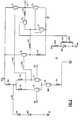
- the circuit shown in Fig. 1 is a push-pull driver 10 including large power driver transistors T1 and T2 connected in series between VCC and VT with the junction of these transistors connected to an output terminal 20.
- a differential cascode current switch predriver of lower power handling transistors includes transistors T3 and T4 coupled as a differential amplifier. The collector of T3 is coupled to node 30 through load resistor R1, and the collector of transistor T4 is connected to node 30 through load resistor R2. Node 30 is connected through resistor R3 to VCC. Node 30 is clamped to ground reference potential VR through a pair of series connected diodes D1 and D2.
- the differential cascode current pair of transistors T3 and T4 have their emitters coupled to a current source comprising transistor T5 and resistor R4 which powers the switch.
- the differential cascode circuit has two wires for input at IN1 and IN2 to transistors T3 and T4 respectively.
- the differential signal at IN1 and IN2 steers the current through the transistors T3 and T4.
- the voltage drop across collector resistor R1 controls the conduction or cutoff of transistor T1 which has its base directly connected to COT node between the transistor T3 and resistor R1.
- the COC node between the resistor R2 and transistor T4 is coupled the base of transistor T6.
- Transistor T6 is coupled as an emitter follower between VCC and VT with a resistor R7 coupled between the emitter of transistor T6 and VT which functions as an emitter follower to voltage VT.
- the emitter follower output at the junction of R7 and transistor T6 is coupled via resistor R8 to the base of the lower of the push-pull power transistor T2.
- a down level clamp is provided by transistors T7 and T8.
- Transistor T7 is coupled as a diode limiter between the base and emitter of the down level power transistor T2. Both the base and collector of transistor T7 is coupled to the base of transistor T2, and the emitter of transistor T7 like T2 is coupled to VT.
- the transistor T8 has the collector coupled to the base of transistor T2 and the emitter to the output node 20 via resistor R9.
- a clamping voltage is provided to the base of transistor T8 to limit the down level to -0.4 volts.
- This down level clamp is provided according to the preferred embodiment off the same diode clamp as the up-level.
- a resistor divider of resistors R5 and R6 are connected in parallel across the lower diode D2.
- a center tap at the required voltage is coupled to the base of transistor T8 to provide a down level clamp that is clamped with respect to reference potential.
- This second clamp could also be as provided in Fig. 2 by a separate VCC to ground circuit.
- a push-pull driver that consumes less power and has faster switching times has been described.
- the push-pull driver is provided by first and second driver transistors connected in series across a source of potential with the emitter of the first transistor and the collector of the second transistor forming the output node.
- a differential current predriver includes a third and fourth transistor with their emitters coupled to a current source. The collector of the third transistor is coupled to the base of the first transistor and the collector of the fourth transistor is coupled to the base of a fifth transistor used as an emitter follower and the emitter of the fifth transistor coupled to the base of the second transistor.
- the collector load resistors of the third and fourth transistors are coupled to a fixed voltage smaller than said source of potential.
Landscapes
- Physics & Mathematics (AREA)
- Engineering & Computer Science (AREA)
- Computer Hardware Design (AREA)
- Computing Systems (AREA)
- General Engineering & Computer Science (AREA)
- Mathematical Physics (AREA)
- Electronic Switches (AREA)
- Logic Circuits (AREA)
Applications Claiming Priority (2)
| Application Number | Priority Date | Filing Date | Title |
|---|---|---|---|
| US07/906,811 US5293083A (en) | 1992-06-30 | 1992-06-30 | Fast limited swing push-pull driver |
| US906811 | 1992-06-30 |
Publications (1)
| Publication Number | Publication Date |
|---|---|
| EP0577286A1 true EP0577286A1 (fr) | 1994-01-05 |
Family
ID=25423018
Family Applications (1)
| Application Number | Title | Priority Date | Filing Date |
|---|---|---|---|
| EP93304661A Withdrawn EP0577286A1 (fr) | 1992-06-30 | 1993-06-15 | Circuit d'attaque push-pull à grande vitesse avec faible amplitude |
Country Status (3)
| Country | Link |
|---|---|
| US (1) | US5293083A (fr) |
| EP (1) | EP0577286A1 (fr) |
| JP (1) | JPH06125263A (fr) |
Families Citing this family (5)
| Publication number | Priority date | Publication date | Assignee | Title |
|---|---|---|---|---|
| US5381057A (en) * | 1993-05-03 | 1995-01-10 | Kabushiki Kaisha Toshiba | ECL gate having active pull-down transistor |
| DE4321483C2 (de) * | 1993-06-28 | 1995-04-20 | Siemens Ag | Leitungstreiberschaltstufe in Stromschaltertechnik |
| DE4321482C1 (de) * | 1993-06-28 | 1994-12-08 | Siemens Ag | Digitale Schaltstufe mit Stromschalter |
| JPH07288464A (ja) * | 1994-04-18 | 1995-10-31 | Toshiba Corp | 半導体集積回路装置 |
| US8982518B2 (en) * | 2013-03-14 | 2015-03-17 | The Boeing Company | Methods and apparatus to provide transient event protection for circuits |
Citations (1)
| Publication number | Priority date | Publication date | Assignee | Title |
|---|---|---|---|---|
| EP0474367A2 (fr) * | 1990-09-04 | 1992-03-11 | International Business Machines Corporation | Circuit d'attaque |
Family Cites Families (10)
| Publication number | Priority date | Publication date | Assignee | Title |
|---|---|---|---|---|
| US4513283A (en) * | 1982-11-30 | 1985-04-23 | International Business Machines Corporation | Latch circuits with differential cascode current switch logic |
| EP0144218B1 (fr) * | 1983-11-30 | 1990-09-05 | Fujitsu Limited | Réseau de portes ECL |
| JP2535813B2 (ja) * | 1985-06-20 | 1996-09-18 | ソニー株式会社 | Ecl−ttl変換出力回路 |
| US4686392A (en) * | 1985-10-30 | 1987-08-11 | International Business Machines Corporation | Multi-functional differential cascode voltage switch logic |
| US4760289A (en) * | 1986-08-04 | 1988-07-26 | International Business Machines Corporation | Two-level differential cascode current switch masterslice |
| JPS63302620A (ja) * | 1987-06-03 | 1988-12-09 | Toshiba Corp | 出力回路 |
| US4874970A (en) * | 1988-05-11 | 1989-10-17 | Applied Micro Circuits Corporation | ECL output with Darlington or common collector-common emitter drive |
| US5013938A (en) * | 1989-11-01 | 1991-05-07 | National Semiconductor Corporation | ECL cutoff driver circuit with reduced stanby power dissipation |
| US5012128A (en) * | 1990-01-24 | 1991-04-30 | International Business Machines Corporation | High speed push-pull driver having current mirror pull-down |
| US5134312A (en) * | 1991-04-25 | 1992-07-28 | Digital Equipment Corporation | Shared current source for alpha particle insensitive bipolar latch |
-
1992
- 1992-06-30 US US07/906,811 patent/US5293083A/en not_active Expired - Fee Related
-
1993
- 1993-05-20 JP JP5118722A patent/JPH06125263A/ja active Pending
- 1993-06-15 EP EP93304661A patent/EP0577286A1/fr not_active Withdrawn
Patent Citations (1)
| Publication number | Priority date | Publication date | Assignee | Title |
|---|---|---|---|---|
| EP0474367A2 (fr) * | 1990-09-04 | 1992-03-11 | International Business Machines Corporation | Circuit d'attaque |
Non-Patent Citations (2)
| Title |
|---|
| IBM TECHNICAL DISCLOSURE BULLETIN vol. 33, no. 1A, June 1990, ARMONK, NY, US pages 311 - 314 ANON 'Cascode logic buffered circuit with regulated push-pull' * |
| PATENT ABSTRACTS OF JAPAN vol. 11, no. 161 (E-509)(2608) 23 May 1987 & JP-A-61 293 022 ( SONY CORP. ) 23 December 1986 * |
Also Published As
| Publication number | Publication date |
|---|---|
| US5293083A (en) | 1994-03-08 |
| JPH06125263A (ja) | 1994-05-06 |
Similar Documents
| Publication | Publication Date | Title |
|---|---|---|
| US5539334A (en) | Method and apparatus for high voltage level shifting | |
| JP3424948B2 (ja) | 低電圧出力駆動器 | |
| US4518876A (en) | TTL-ECL Input translation with AND/NAND function | |
| US4311927A (en) | Transistor logic tristate device with reduced output capacitance | |
| EP0196113B1 (fr) | Circuit tampon à trois états | |
| US3660675A (en) | Transmission line series termination network for interconnecting high speed logic circuits | |
| US4931672A (en) | True TTL to true ECL bi-directional tristatable translator driver circuit | |
| US4943740A (en) | Ultra fast logic | |
| EP0577286A1 (fr) | Circuit d'attaque push-pull à grande vitesse avec faible amplitude | |
| EP0417786A2 (fr) | Circuit de translation de niveaux à vitesse de traitement élevée et possibilité de courant de sortie améliorée | |
| EP0320582B1 (fr) | Circuit d'attaque bicmos comportant une source de tension intégrée submicronique | |
| JPH0783247B2 (ja) | インタフエース受信回路及びレベル変換回路 | |
| US5142168A (en) | Emitter-coupled logic balanced signal transmission circuit | |
| EP0590247A2 (fr) | Circuit BICMOS de conversion de niveau | |
| JP3949443B2 (ja) | ディセーブルオプションを有する変換スイッチ回路 | |
| EP0438953A1 (fr) | Circuit d'attaque push-pull à grande vitesse avec miroir de courant de tirage vers le bas | |
| US4481481A (en) | Buffer inverter circuit with adaptive bias | |
| JPH03195120A (ja) | 半導体出力回路 | |
| US4835455A (en) | Reference voltage generator | |
| US5124591A (en) | Low power push pull driver | |
| US6002288A (en) | Current limiting circuit and method that may be shared among different circuitry | |
| US4458159A (en) | Large swing driver/receiver circuit | |
| JPH0659028B2 (ja) | 論理回路 | |
| EP0440055A2 (fr) | Circuit tampon TTL inverseur à hystérésis et à haute vitesse | |
| EP0476341B1 (fr) | Circuit logique BICMOS avec une sortie CML |
Legal Events
| Date | Code | Title | Description |
|---|---|---|---|
| PUAI | Public reference made under article 153(3) epc to a published international application that has entered the european phase |
Free format text: ORIGINAL CODE: 0009012 |
|
| AK | Designated contracting states |
Kind code of ref document: A1 Designated state(s): DE FR GB |
|
| 17P | Request for examination filed |
Effective date: 19940429 |
|
| STAA | Information on the status of an ep patent application or granted ep patent |
Free format text: STATUS: THE APPLICATION HAS BEEN WITHDRAWN |
|
| 18W | Application withdrawn |
Withdrawal date: 19960506 |