US5293083A - Fast limited swing push-pull driver - Google Patents
Fast limited swing push-pull driver Download PDFInfo
- Publication number
- US5293083A US5293083A US07/906,811 US90681192A US5293083A US 5293083 A US5293083 A US 5293083A US 90681192 A US90681192 A US 90681192A US 5293083 A US5293083 A US 5293083A
- Authority
- US
- United States
- Prior art keywords
- transistor
- base
- potential
- source
- providing
- Prior art date
- Legal status (The legal status is an assumption and is not a legal conclusion. Google has not performed a legal analysis and makes no representation as to the accuracy of the status listed.)
- Expired - Fee Related
Links
Images

Classifications
-
- H—ELECTRICITY
- H03—ELECTRONIC CIRCUITRY
- H03K—PULSE TECHNIQUE
- H03K19/00—Logic circuits, i.e. having at least two inputs acting on one output; Inverting circuits
- H03K19/01—Modifications for accelerating switching
- H03K19/013—Modifications for accelerating switching in bipolar transistor circuits
-
- H—ELECTRICITY
- H03—ELECTRONIC CIRCUITRY
- H03K—PULSE TECHNIQUE
- H03K19/00—Logic circuits, i.e. having at least two inputs acting on one output; Inverting circuits
- H03K19/0008—Arrangements for reducing power consumption
- H03K19/001—Arrangements for reducing power consumption in bipolar transistor circuits
Definitions
- This invention relates to push-pull drivers and more particularly to a driver that consumes less power and has faster switching speed.
- differential cascode current switch circuitry is well known, as disclosed in U.S. Pat. No. 4,513,283 of Lininger entitled “Latch Circuits with Differential Cascode Current Switch Logic", U.S. Pat. No. 4,760,289 of Eichelberger et al. entitled “Two Level Differential Cascode Current Switch Masterslice” and U.S. Pat. No. 4,686,392 of Lo.
- the driver used herein is particularly for use with differential cascode circuitry which requires less current and is lower power than ECL (Emitter Coupled Logic) circuitry.
- the logic is provided by a pair of wires, and for a logic "1" level, 0.6 volts is on one lead and 0.4 volts is on the other lead, and for a logic "0", the levels are reversed. A 20 percent increase in performance is believed to be achieved using this differential cascode current switch as compared to an ECL masterslice running the same power.
- a two level differential cascode driver is also disclosed in Chu et al., U.S. Pat. No. 5,124,591 issued Jun. 23, 1992, entitled “Low Power Push Pull Driver”, incorporated herein by reference (case has been allowed).
- a push-pull driver that consumes less power and has faster switching times is provided by first and second driver transistors connected in series across a source of potential with the emitter of the first transistor and the collector of the second transistor forming the output node.
- a differential current predriver includes a third and fourth transistor with their emitters coupled to a current source. The collector of the third transistor is coupled to the base of the first transistor and the collector of the fourth transistor is coupled to the base of a fifth transistor used as an emitter follower and the emitter of the fifth transistor coupled to the base of the second transistor.
- the collector load resistors of the third and fourth transistors are coupled to a fixed voltage smaller than said source of potential.
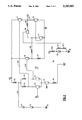
- FIG. 1 is a schematic diagram of the invention in accordance with the preferred embodiment of the present invention.
- FIG. 2 is a schematic diagram of the invention in accordance with an alternative embodiment of the present invention.
- the circuit shown in FIG. 1 is a push-pull driver 10 including large power driver transistors T1 and T2 connected in series between VCC and VT with the junction of these transistors connected to an output terminal 20.
- a differential cascode current switch predriver of lower power handling transistors includes transistors T3 and T4 coupled as a differential amplifier. The collector of T3 is coupled to node 30 through load resistor R1, and the collector of transistor T4 is connected to node 30 through load resistor R2. Node 30 is connected through resistor R3 to VCC. Node 30 is clamped to ground reference potential VR through a pair of series connected diodes D1 and D2.
- the differential cascode current pair of transistors T3 and T4 have their emitters coupled to a current source comprising transistor T5 and resistor R4 which powers the switch.
- the differential cascode circuit has two wires for input at IN1 and IN2 to transistors T3 and T4 respectively.
- the differential signal at IN1 and IN2 steers the current through the transistors T3 and T4.
- the voltage drop across collector resistor R1 controls the conduction or cutoff of transistor T1 which has its base directly connected to COT node between the transistor T3 and resistor R1.
- the COC node between the resistor R2 and transistor T4 is coupled the base of transistor T6.
- Transistor T6 is coupled as an emitter follower between VCC and VT with a resistor R7 coupled between the emitter of transistor T6 and VT which functions as an emitter follower to voltage VT.
- the emitter follower output at the junction of R7 and transistor T6 is coupled via resistor R8 to the base of the lower of the push-pull power transistor T2.
- a down level clamp is provided by transistors T7 and T8.
- Transistor T7 is coupled as a diode limiter between the base and emitter of the down level power transistor T2. Both the base and collector of transistor T7 is coupled to the base of transistor T2, and the emitter of transistor T7 like T2 is coupled to VT.
- the transistor T8 has the collector coupled to the base of transistor T2 and the emitter to the output node 20 via resistor R9.
- a clamping voltage is provided to the base of transistor T8 to limit the down level to -0.4 volts.
- This down level clamp is provided according to the preferred embodiment off the same diode clamp as the up-level.
- a resistor divider of resistors R5 and R6 are connected in parallel across the lower diode D2.
- a center tap at the required voltage is coupled to the base of transistor T8 to provide a down level clamp that is clamped with respect to reference potential.
- This second clamp could also be as provided in FIG. 2 by a separate VCC to ground circuit.
- circuit elements had the following values: ##EQU1##
- the improvement is achieved by controlling the up-level by clamping the collector common node 30 with respect to output signal reference VR to less than VCC.
- the collector resistors are smaller so there is smaller signal swing and the operation is faster. A smaller signal swing is tolerated because the node is clamped with respect to output signal reference.
- the resistor divider second clamped node is designed to limit the output to a smaller signal swing which makes the switching faster and is tolerated because the reference is again with respect to reference voltage VR at ground. Because this second clamp is using the same clamping source, it uses less power.
Landscapes
- Physics & Mathematics (AREA)
- Engineering & Computer Science (AREA)
- Computer Hardware Design (AREA)
- Computing Systems (AREA)
- General Engineering & Computer Science (AREA)
- Mathematical Physics (AREA)
- Electronic Switches (AREA)
- Logic Circuits (AREA)
Priority Applications (3)
| Application Number | Priority Date | Filing Date | Title |
|---|---|---|---|
| US07/906,811 US5293083A (en) | 1992-06-30 | 1992-06-30 | Fast limited swing push-pull driver |
| JP5118722A JPH06125263A (ja) | 1992-06-30 | 1993-05-20 | 高速振幅制限プッシュ・プル・ドライバ |
| EP93304661A EP0577286A1 (fr) | 1992-06-30 | 1993-06-15 | Circuit d'attaque push-pull à grande vitesse avec faible amplitude |
Applications Claiming Priority (1)
| Application Number | Priority Date | Filing Date | Title |
|---|---|---|---|
| US07/906,811 US5293083A (en) | 1992-06-30 | 1992-06-30 | Fast limited swing push-pull driver |
Publications (1)
| Publication Number | Publication Date |
|---|---|
| US5293083A true US5293083A (en) | 1994-03-08 |
Family
ID=25423018
Family Applications (1)
| Application Number | Title | Priority Date | Filing Date |
|---|---|---|---|
| US07/906,811 Expired - Fee Related US5293083A (en) | 1992-06-30 | 1992-06-30 | Fast limited swing push-pull driver |
Country Status (3)
| Country | Link |
|---|---|
| US (1) | US5293083A (fr) |
| EP (1) | EP0577286A1 (fr) |
| JP (1) | JPH06125263A (fr) |
Cited By (5)
| Publication number | Priority date | Publication date | Assignee | Title |
|---|---|---|---|---|
| US5381057A (en) * | 1993-05-03 | 1995-01-10 | Kabushiki Kaisha Toshiba | ECL gate having active pull-down transistor |
| US5473272A (en) * | 1993-06-28 | 1995-12-05 | Siemens Aktiengesellschaft | Digital differential amplifier switching stage with current switch |
| US5539350A (en) * | 1993-06-28 | 1996-07-23 | Siemens Aktiengesellschaft | Common mode logic line driver switching stage |
| US5684416A (en) * | 1994-04-18 | 1997-11-04 | Kabushiki Kaisha Toshiba | Low voltage bipolar transistor logic circuit |
| US8982518B2 (en) * | 2013-03-14 | 2015-03-17 | The Boeing Company | Methods and apparatus to provide transient event protection for circuits |
Citations (11)
| Publication number | Priority date | Publication date | Assignee | Title |
|---|---|---|---|---|
| US4513283A (en) * | 1982-11-30 | 1985-04-23 | International Business Machines Corporation | Latch circuits with differential cascode current switch logic |
| JPS61293022A (ja) * | 1985-06-20 | 1986-12-23 | Sony Corp | Ecl−ttl変換出力回路 |
| US4686392A (en) * | 1985-10-30 | 1987-08-11 | International Business Machines Corporation | Multi-functional differential cascode voltage switch logic |
| US4760289A (en) * | 1986-08-04 | 1988-07-26 | International Business Machines Corporation | Two-level differential cascode current switch masterslice |
| US4866303A (en) * | 1983-11-30 | 1989-09-12 | Fujitsu Limited | ECL gate array with collector resistance compensation for distance from power supply pad |
| US4874970A (en) * | 1988-05-11 | 1989-10-17 | Applied Micro Circuits Corporation | ECL output with Darlington or common collector-common emitter drive |
| US4906869A (en) * | 1987-06-03 | 1990-03-06 | Kabushiki Kaisha Toshiba | Output circuit having wide range frequency response characteristic |
| US5012128A (en) * | 1990-01-24 | 1991-04-30 | International Business Machines Corporation | High speed push-pull driver having current mirror pull-down |
| US5013938A (en) * | 1989-11-01 | 1991-05-07 | National Semiconductor Corporation | ECL cutoff driver circuit with reduced stanby power dissipation |
| EP0474367A2 (fr) * | 1990-09-04 | 1992-03-11 | International Business Machines Corporation | Circuit d'attaque |
| US5134312A (en) * | 1991-04-25 | 1992-07-28 | Digital Equipment Corporation | Shared current source for alpha particle insensitive bipolar latch |
-
1992
- 1992-06-30 US US07/906,811 patent/US5293083A/en not_active Expired - Fee Related
-
1993
- 1993-05-20 JP JP5118722A patent/JPH06125263A/ja active Pending
- 1993-06-15 EP EP93304661A patent/EP0577286A1/fr not_active Withdrawn
Patent Citations (12)
| Publication number | Priority date | Publication date | Assignee | Title |
|---|---|---|---|---|
| US4513283A (en) * | 1982-11-30 | 1985-04-23 | International Business Machines Corporation | Latch circuits with differential cascode current switch logic |
| US4866303A (en) * | 1983-11-30 | 1989-09-12 | Fujitsu Limited | ECL gate array with collector resistance compensation for distance from power supply pad |
| JPS61293022A (ja) * | 1985-06-20 | 1986-12-23 | Sony Corp | Ecl−ttl変換出力回路 |
| US4686392A (en) * | 1985-10-30 | 1987-08-11 | International Business Machines Corporation | Multi-functional differential cascode voltage switch logic |
| US4760289A (en) * | 1986-08-04 | 1988-07-26 | International Business Machines Corporation | Two-level differential cascode current switch masterslice |
| US4906869A (en) * | 1987-06-03 | 1990-03-06 | Kabushiki Kaisha Toshiba | Output circuit having wide range frequency response characteristic |
| US4874970A (en) * | 1988-05-11 | 1989-10-17 | Applied Micro Circuits Corporation | ECL output with Darlington or common collector-common emitter drive |
| US5013938A (en) * | 1989-11-01 | 1991-05-07 | National Semiconductor Corporation | ECL cutoff driver circuit with reduced stanby power dissipation |
| US5012128A (en) * | 1990-01-24 | 1991-04-30 | International Business Machines Corporation | High speed push-pull driver having current mirror pull-down |
| EP0474367A2 (fr) * | 1990-09-04 | 1992-03-11 | International Business Machines Corporation | Circuit d'attaque |
| US5124591A (en) * | 1990-09-04 | 1992-06-23 | International Business Machines Corporation | Low power push pull driver |
| US5134312A (en) * | 1991-04-25 | 1992-07-28 | Digital Equipment Corporation | Shared current source for alpha particle insensitive bipolar latch |
Non-Patent Citations (2)
| Title |
|---|
| IBM Tech. Disclosure Bulletin, vol. 33, No. 1A, Jun. 1990 "Cascode Logic Buffered Circuit with Regulated Push-Pull". |
| IBM Tech. Disclosure Bulletin, vol. 33, No. 1A, Jun. 1990 Cascode Logic Buffered Circuit with Regulated Push Pull . * |
Cited By (6)
| Publication number | Priority date | Publication date | Assignee | Title |
|---|---|---|---|---|
| US5381057A (en) * | 1993-05-03 | 1995-01-10 | Kabushiki Kaisha Toshiba | ECL gate having active pull-down transistor |
| US5473272A (en) * | 1993-06-28 | 1995-12-05 | Siemens Aktiengesellschaft | Digital differential amplifier switching stage with current switch |
| US5539350A (en) * | 1993-06-28 | 1996-07-23 | Siemens Aktiengesellschaft | Common mode logic line driver switching stage |
| US5684416A (en) * | 1994-04-18 | 1997-11-04 | Kabushiki Kaisha Toshiba | Low voltage bipolar transistor logic circuit |
| US8982518B2 (en) * | 2013-03-14 | 2015-03-17 | The Boeing Company | Methods and apparatus to provide transient event protection for circuits |
| TWI619323B (zh) * | 2013-03-14 | 2018-03-21 | 波音公司 | 提供用於電路之暫態事件保護的方法、設備及電腦可讀取儲存媒體 |
Also Published As
| Publication number | Publication date |
|---|---|
| EP0577286A1 (fr) | 1994-01-05 |
| JPH06125263A (ja) | 1994-05-06 |
Similar Documents
| Publication | Publication Date | Title |
|---|---|---|
| US4255670A (en) | Transistor logic tristate output with feedback | |
| JP3424948B2 (ja) | 低電圧出力駆動器 | |
| US4311927A (en) | Transistor logic tristate device with reduced output capacitance | |
| US4518876A (en) | TTL-ECL Input translation with AND/NAND function | |
| US4112314A (en) | Logical current switch | |
| US4943740A (en) | Ultra fast logic | |
| US4931672A (en) | True TTL to true ECL bi-directional tristatable translator driver circuit | |
| EP0590247B1 (fr) | Circuit BICMOS de conversion de niveau | |
| US5293083A (en) | Fast limited swing push-pull driver | |
| EP0320582B1 (fr) | Circuit d'attaque bicmos comportant une source de tension intégrée submicronique | |
| JPH0783247B2 (ja) | インタフエース受信回路及びレベル変換回路 | |
| US5012128A (en) | High speed push-pull driver having current mirror pull-down | |
| US4587494A (en) | Quasi-complementary class B IC output stage | |
| EP0055341A2 (fr) | Porte logique commandée par le courant | |
| EP0207962B1 (fr) | Circuit de commande a trois etats | |
| JPH03195120A (ja) | 半導体出力回路 | |
| JP2002252556A (ja) | ディセーブルオプションを有する変換スイッチ回路 | |
| US5021687A (en) | High speed inverting hysteresis TTL buffer circuit | |
| US5124591A (en) | Low power push pull driver | |
| US4458159A (en) | Large swing driver/receiver circuit | |
| US6002288A (en) | Current limiting circuit and method that may be shared among different circuitry | |
| JPH0659028B2 (ja) | 論理回路 | |
| EP0476341B1 (fr) | Circuit logique BICMOS avec une sortie CML | |
| US5311082A (en) | CMOS to ECL level translator | |
| US5258661A (en) | High noise tolerance receiver |
Legal Events
| Date | Code | Title | Description |
|---|---|---|---|
| AS | Assignment |
Owner name: INTERNATIONAL BUSINESS MACHINES CORPORATION, A COR Free format text: ASSIGNMENT OF ASSIGNORS INTEREST.;ASSIGNORS:ASKIN, HALUK O.;HUI, DAVID T.;SALIMI, BIJAN;AND OTHERS;REEL/FRAME:006238/0284;SIGNING DATES FROM 19920728 TO 19920811 |
|
| FEPP | Fee payment procedure |
Free format text: PAYOR NUMBER ASSIGNED (ORIGINAL EVENT CODE: ASPN); ENTITY STATUS OF PATENT OWNER: LARGE ENTITY |
|
| REMI | Maintenance fee reminder mailed | ||
| LAPS | Lapse for failure to pay maintenance fees | ||
| FP | Lapsed due to failure to pay maintenance fee |
Effective date: 19980311 |
|
| FEPP | Fee payment procedure |
Free format text: PAYER NUMBER DE-ASSIGNED (ORIGINAL EVENT CODE: RMPN); ENTITY STATUS OF PATENT OWNER: LARGE ENTITY Free format text: PAYOR NUMBER ASSIGNED (ORIGINAL EVENT CODE: ASPN); ENTITY STATUS OF PATENT OWNER: LARGE ENTITY |
|
| STCH | Information on status: patent discontinuation |
Free format text: PATENT EXPIRED DUE TO NONPAYMENT OF MAINTENANCE FEES UNDER 37 CFR 1.362 |