EP0579413B1 - Dynamische Steuerung der Belichtung individueller Punkte in einer optischen Ausgabeeinrichtung - Google Patents
Dynamische Steuerung der Belichtung individueller Punkte in einer optischen Ausgabeeinrichtung Download PDFInfo
- Publication number
- EP0579413B1 EP0579413B1 EP93305104A EP93305104A EP0579413B1 EP 0579413 B1 EP0579413 B1 EP 0579413B1 EP 93305104 A EP93305104 A EP 93305104A EP 93305104 A EP93305104 A EP 93305104A EP 0579413 B1 EP0579413 B1 EP 0579413B1
- Authority
- EP
- European Patent Office
- Prior art keywords
- light
- spot
- laser
- light source
- optical
- Prior art date
- Legal status (The legal status is an assumption and is not a legal conclusion. Google has not performed a legal analysis and makes no representation as to the accuracy of the status listed.)
- Expired - Lifetime
Links
Images


Classifications
-
- G—PHYSICS
- G06—COMPUTING OR CALCULATING; COUNTING
- G06K—GRAPHICAL DATA READING; PRESENTATION OF DATA; RECORD CARRIERS; HANDLING RECORD CARRIERS
- G06K15/00—Arrangements for producing a permanent visual presentation of the output data, e.g. computer output printers
- G06K15/02—Arrangements for producing a permanent visual presentation of the output data, e.g. computer output printers using printers
- G06K15/12—Arrangements for producing a permanent visual presentation of the output data, e.g. computer output printers using printers by photographic printing, e.g. by laser printers
- G06K15/1204—Arrangements for producing a permanent visual presentation of the output data, e.g. computer output printers using printers by photographic printing, e.g. by laser printers involving the fast moving of an optical beam in the main scanning direction
- G06K15/1209—Intensity control of the optical beam
- G06K15/1214—Intensity control of the optical beam by feedback
Definitions
- the present invention relates generally to the field of optical output devices, and more specifically to a method and apparatus for accurately controlling the optical energy delivered to a photoreceptive element in a raster output scanning system.
- the polygon is rotated about an axis while an intensity-modulated light beam, typically laser light, is brought to bear on the rotating polygon at a predetermined angle.
- the light beam is reflected by a facet and thereafter focussed to a "spot" on a photosensitive recording medium.
- the rotation of the polygon causes the spot to scan linearly across the photosensitive medium in a fast scan (i.e., line scan) direction.
- the photosensitive medium is advanced relatively more slowly than the rate of the fast scan in a slow scan direction which is orthogonal to the fast scan direction. In this way, the beam scans the recording medium in a raster scanning pattern.
- FIG. 3 shows a side or elevation view of the general optical configuration of an apparatus according to another embodiment of the present invention, showing a linear array of diode lasers as the light source for a typical ROS system and positions of two of the emitted laser spots imaged on the photoreceptive surface during a single scan.
- FIG. 4 shows one embodiment of a single diode laser integrated with an optical detector for monitoring the time varying power output of the laser.
- FIG. 6 shows a functional diagram of one embodiment of the electrical apparatus used to control the energy content of a single optical pulse emitted by the laser for the purposes of the present invention.
- FIG. 7 shows a functional diagram of a third embodiment of the electrical apparatus used to control the energy content of a single optical pulse emitted by the laser for the purposes of the present invention.
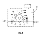
- FIG. 9 shows a schematic diagram for a complete xerographic print engine employing the exposure control method and apparatus of the present invention.
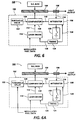
- FIGS. 1 and 2 show, respectively, slow scan plane and fast scan plane views of a scanning apparatus 10.
- Apparatus 10 is a raster output scanning device of the type which may, for example, output a scanned modulated optical signal to a photoreceptive drum 12, such as that shown in FIG. 1A, for use in a xerographic printing process.
- apparatus 10 may output a scanned modulated optical signal to a display device, a photographic device or other application employing such a scanned modulated optical signal.
- Beam 16 is reflected by facet 26 so as to pass through compound spherical lens 28. Since the beam converges on facet 26, upon reflection it diverges. Therefore, lenses 28 and 30 are employed to refocus the beam to a circular or elliptical cross-section onto image plane 32, and to correct for scan nonlinearity (f-theta correction).
- Toroidal lens 30, or an equivalent thereto (such as a cylindrical mirror) further corrects for wobble (scanner motion or facet errors) as known in the art.
- a beam reflected from one of its moving facets will be caused to scan across the image plane 32, as indicated by the arrow B.
- modulating the beam for example by modulating the current applied to the laser itself from below to above the lasing threshold, as known in the art, a scanned modulated single beam of general application results.
- the image plane 32 comprises the line on the rotating photoreceptive drum 12 of FIG. 1A, and the rotation of drum 12 and the modulation and scanning of the beam are properly coordinated, a ROS printer device may be realized.
- Fig. 3 shows an embodiment of the present invention allowing simultaneous modulated scanning for a plurality of spots.
- apparatus 40 includes multiple light sources 54a, 54b, such as independent solid state lasers, or the emitters of a monolithic multiple beam solid state laser, which produce independent beams of coherent light 62a, 62b.
- beams 62a and 62b pass through spherical lens 18 which collimates the beams in the fast and slow scan planes.
- the collimated beams then pass through a cylindrical lens 20, so that they illuminate a facet 26 of scanning device 24.
- the detector can be any one of a number of different types as described in EP-A-0 449,636, or other types known to those skilled in the art.
- the detector directly samples either the light power internal to the laser cavity, in the case of a monolithic detector, or the light power emitted by the laser, in the case of a nonmonolithic detector, to allow obtaining an output signal which is a known representation of, or proportional to, the time-dependent optical output of the laser.
- the current drive signal is a pulse modulation representation of the data to be printed and drives the laser to provide an output light beam modulated in accordance with this data.
- the output signal of the photodetector of either monolithic or nonmonolithic type, is an electrical signal which is most commonly but not necessarily proportional to the variation of the amplitude of the output light beam during each pulse. This output signal is employed to further control the modulation of the light source as described below.
- FIG. 6 is a schematic illustration detailing a first embodiment of an apparatus for controlling the modulation of a light source in an optical output system 100.
- apparatus 102 is employed in conjunction with a light source such as laser 104 and a photodetector 106.
- Apparatus 102 includes an integrator circuit 108 and a comparator circuit 110.
- a laser drive signal 112 from laser driver 114 which represents the modulated pixel data to be written onto the photoreceptive medium, is input to the comparator 110.
- Integrator circuit 108 receives the output photocurrent 116 from detector 106 and produces as its output signal 118 the time-integrated value of the photocurrent.
- Photocurrent 116 which is an electrical signal representative of the time-varying amplitude of the output light beam from laser 104, is integrated over time by integrator circuit 108 by any one of a large number of methods well known to those skilled in the art.
- the output signal of the integrator is proportional to the total energy E(t) emitted by the laser 104 from the beginning of the pulse up to time t, i.e., where P(t') is the power emitted by the laser at time t' and K is a proportionality constant.
- the output signal 118 is input to comparator circuit 110.
- the comparator circuit 110 operates in such a manner that when the voltage of the integrator output signal 118 is less than the threshold value 120 the laser drive signal 112 is permitted to drive laser 104, but when the voltage of the integrator signal 118 is equal to or exceeds the threshold value 120 the laser pulsed drive signal 112 is switched off from laser 104, thus limiting the energy forming the spot on the photoreceptive medium.
- Apparatus 102 of Fig. 6 may thus, in conjunction with laser source 104 and detector 106, control the duration of the optical pulse emitted by the laser source 104, and thus control for example the size of the spot formed on the photosensitive medium.
- Timing circuit 124 produces timing signals 126 and 128 which are input to laser driver 114 and integrator 108.
- the timing signal sequences the laser driver 114 such that the integrator 108 may be reset by reset circuit 130, for example by shorting the integrator to ground, without interfering with the comparison done by comparator circuit 110.
- control of the modulation of the light source is performed by operating the laser in conjunction with an electrical apparatus 202 consisting of an integrator circuit 204, a comparator circuit 206, a trigger circuit 208, and the laser drive circuit 210.
- the integration circuit 204 produces an electrical output signal, which is the time integral of the photocurrent 212 from detector 106, by methods known in the art.
- the integral valued electrical output signal 214 from integrator 204 is input to the comparator circuit 206, which compares the output signal 214 to a threshold value 216 from threshold value circuit 218.
- Apparatus 202 of Fig. 7 may thus, in conjunction with laser source 104 and detector 106, control the duration of the optical pulse emitted by the laser source 104, and thus control for example the size of the spot formed on the photosensitive medium.
- Timing circuit 226 produces timing signals 228 and 230 which are input to trigger circuit 208 and integrator circuit 204.
- the timing signal sequences the trigger circuit 208 such that the integrator 204 may be reset by reset circuit 232, for example by shorting the integrator circuit 204 to ground, without interfering with the comparison done by comparator circuit 206.
- FIGS. 8A through 8D shows waveforms of the output signals at different points in apparatus 202 of FIG. 7.
- FIG 8A shows the photocurrent 212 from the photodetector 90, and is an electrical representation of the optical output of the laser 78 for three types of time-varying pulses.
- Pulse 302a illustrates a first type of pulse wherein the amplitude is decreasing during the pulse (positive droop).
- Pulse 302b illustrates a second type of pulse wherein the amplitude is constant during the pulse (no droop).
- Pulse 302c illustrates a third type of pulse wherein the amplitude is increasing during the pulse (negative droop).
- FIG. 8B shows the integrated detector output corresponding to each of the types of pulses shown in FIG.
- the waveforms shown in FIG. 8C are the trigger signals generated when the modulated pixel data initiates a new current pulse which lasts until waveform 304a, 304b, 304c reaches the threshold value 306.
- the waveforms shown in FIG. 8C represent the output of the trigger circuit 208 corresponding to each of the waveforms in FIGS. 8A and 8B.
- 8D are the amplitude of the laser drive current 224, where the start of each waveform 310a, 310b, 310c is initiated by the switch of the trigger output signal 222 from low to high followed by termination when the trigger output signal 222 switches from high to low.
- the threshold signal 216 which is input to the comparator determines the amount of energy to be delivered to the photoreceptor in a pulse and is set by the information data to be printed. Since the amount of energy in a pulse determines the exposure level of the image, e.g. the areal size of the exposure on a xerographic photoreceptor, holding the threshold value constant from pulse to pulse accurately maintains a fixed exposure condition during the scan in the presence of time variations in the laser's output intensity that arise from fluctuations in the laser's temperature or other variables affecting the laser's output intensity.
- the energy content of each pulse and consequently the exposure level in the case of a xerographic image can be accurately varied by changing the threshold value from pulse to pulse despite variations in the laser output that might arise from temperature fluctuations, varying drive current pulse width, etc.
- Such variation of the exposure level of the photoreceptor may be useful to compensate for decreasing sensitivity of the photoreceptor resulting from prolonged use, or to create desired output effects.
- the electrical apparatus 102 or 202 can be a separate electrical component used in conjunction with a single laser source or a monolithic array of laser emitters.
- it may be constructed as a silicon or GaAs integrated circuit connected to the laser as is well known in the art.
- detector 90 can be an integral part of the integrated circuit.
- optical source 14 (FIG. 1) is an array of closely spaced lasers, a preferred embodiment is to integrate the detector and the laser into a monolithic apparatus as disclosed in the aforementioned EP-A-0,449,636.
- Apparatus 102 or 202 may alternatively be monolithically integrated with either a single laser source or a monolithic array of lasers.
- optical energy control may be achieved on a spot-by-spot basis.
- a spot exposure time is on the order of 14 nanoseconds.
- Proper selection and design of electrical circuits and interconnections for the electrical apparatus of the present invention will allow switching speeds of 1 nanosecond or faster, thus facilitating spot-to-spot control of the optical energy.
- the present invention operates equally well, and without significant modification, to control exposure in a single beam ROS or in a multiple beam ROS
- the apparatus and method of the present invention may be combined with other apparatus and/or methods of modulating the output beam of a diode laser to achieve advantageous results.
- the inventions of EP-A-0,493,104 and of our copending European patent application EP-A-558 220 may be employed herewith such that the content of all pulses emitted from a multiple laser array are accurately controlled.
Landscapes
- Physics & Mathematics (AREA)
- Engineering & Computer Science (AREA)
- Optics & Photonics (AREA)
- General Engineering & Computer Science (AREA)
- General Physics & Mathematics (AREA)
- Theoretical Computer Science (AREA)
- Laser Beam Printer (AREA)
- Control Of Exposure In Printing And Copying (AREA)
- Exposure And Positioning Against Photoresist Photosensitive Materials (AREA)
- Exposure Of Semiconductors, Excluding Electron Or Ion Beam Exposure (AREA)
- Mechanical Optical Scanning Systems (AREA)
Claims (8)
- Verfahren zum Steuern eines optischen Ausgabegerätes (100,200), um ein Bild zu erzeugen, wobei das Verfahren folgende Schritte umfaßt:dadurch gekennzeichnet, daß das Verfahren weiterhin umfaßt das Modulieren der erzeugten Lichts in Übereinstimmung mit einem Impuls-Bilddatensignal (112;224), wobei das modulierten Licht eine Vielzahl von individuellen Lichtimpulsen umfaßt, und das Erzeugen des Steuersignals (220) zum Steuern der optischen Energie, die jeweils zu jedem Punkt des Bildes geliefert wird, indem das während der Bestrahlung des Punktes erzeugte Zeitintegral mit dem Inhalt eines Schwellwertspeichers (122;218) unabhängig von der durch die Lichtquelle (104) emittierten optischen Intensität verglichen wird.Erzeugen von Licht aus einer Lichtquelle (104),Ablesen von wenigstens einem Teil des Lichts,Umwandeln des abgelesenen Lichts zu einem Photostrom (116;212),Berechnen des Zeitintegrals des Photostroms (116;212)Vergleichen des Zeitintegrals mit einem Schwellwert, um ein Steuersignal zu erzeugen, undBeenden des Lichts aus der Lichtquelle (104) in Übereinstimmung mit dem Steuersignal (220),
- Verfahren nach Anspruch 1, wobei die Lichtquelle (104) ein Festkörperlaser ist und wobei der Schritt zum Beenden des Lichts aus der Lichtquelle das Anlegen eines Stroms unter dem Schwellwert des Lasers an dem Laser umfaßt.
- Verfahren nach Anspruch 1 oder 2, das das Synchronisieren der Lichtquelle (104) und des Steuersignals (220) umfaßt, so das Beenden des Lichts aus der Lichtquelle (104) für einen Punkt nicht die Modulation der erzeugten Lichts in Übereinstimmung mit dem Datensignal für einen anderen Punkt beeinflußt.
- Vorrichtung zum Steuern eines optischen Ausgabeeinrichtung (100;200), um ein Bild zu erzeugen, wobei die Vorrichtung umfaßt:dadurch gekennzeichnet, daß die Vorrichtung weiterhin umfaßt eine Modulationseinrichtung (114;210) zum Modulieren des erzeugten Lichts in Übereinstimmung mit einem Impuls-Bilddatensignal, wobei das modulierte Licht eine Vielzahl von einzelnen Lichtimpulsen umfaßt, eine Schwellwertspeichereinrichtung (122,218) und eine Vergleichereinrichtung (110;206) zum Vergleichen des während der Bestrahlung jedes Punkts erzeugten Zeitintegrals mit den Inhalten des Schwellwertspeichers (122; 218) unabhängig von der durch die Lichtquelle (104) emittierten optischen Intensität, wobei die Vergleichereinrichtung (110;206) ein Steuersignal (220) zum Steuern der zu jedem Punkt des Bildes gelieferten optischen Energie erzeugt, indem sie das Licht (116) aus der Lichtquelle (104) beendet.eine Lichtquelle (104),eine Photodetektoreinrichtung (106) zum Ablesen wenigstens eines Teils des modulierten Lichts und zum Umwandeln desselben zu einem Photostrom (116;212),eine Integrationseinrichtung (108;204) zum Berechnen des Zeitintegrals des Photostroms (116;212), undeine Einrichtung zum Vergleichen des Zeitintegrals mit einem Schwellwert,
- Vorrichtung nach Anspruch 4, wobei die Lichtquelle (104) ein Festkörperlaser ist und wobei die Modulationseinrichtung (114;210) eine Stromversorgung ist, die geschaltet werden kann, um den an dem Laser angelegten Strom von einem Wert unter dem Schwellwert zu einem Wert über dem Schwellwert des Lasers zu variieren, wobei das Steuersignal den an dem Laser angelegten Strom schaltet, so daß er unter dem Schwellwert des Lasers ist.
- Vorrichtung nach Anspruch 4 oder 5, wobei die Lichtquelle (104) und das Steuersignal (220) synchronisiert sind, so daß das Licht aus der Lichtquelle (104) für einen Punkt nicht die Modulation des erzeugten Lichts in Übereinstimmung mit dem Datensignal für einen anderen Punkt beeinflußt.
- Vorrichtung nach wenigstens einem der Ansprüche 4 bis 6, die ein photorezeptives Medium umfaßt, auf dem ein Punkt gebildet wird, wobei der Inhalt des Schwellwertspeichers (122;218) wenigstens den Wert des zeitintegrierten Photostroms umfaßt, der erforderlich ist, um eine gewünschte Punktbelichtung auf dem photorezeptiven Medium zu erzeugen.
- Vorrichtung nach Anspruch 7, wobei der Schwellwertspeicher (122;218) mehrere Werte enthält, wobei jedes Wert einer unterschiedlichen Punktbelichtung entspricht, wobei jedem auf dem photorezeptiven Medium zu bildenden Punkt einer der Werte aus dem Schwellwertspeicher (122,218) zugewiesen wird, wobei der für jeden Punkt zugewiesene Wert vor dem Vergleich des ausgewählten Schwellwerts mit dem zeitintegrierten Photostrom an den Schwellwertspeicher (122;218) kommuniziert wird.
Applications Claiming Priority (2)
| Application Number | Priority Date | Filing Date | Title |
|---|---|---|---|
| US07/906,145 US5497181A (en) | 1992-06-29 | 1992-06-29 | Dynamic control of individual spot exposure in an optical output device |
| US906145 | 1992-06-29 |
Publications (2)
| Publication Number | Publication Date |
|---|---|
| EP0579413A1 EP0579413A1 (de) | 1994-01-19 |
| EP0579413B1 true EP0579413B1 (de) | 1998-07-22 |
Family
ID=25421998
Family Applications (1)
| Application Number | Title | Priority Date | Filing Date |
|---|---|---|---|
| EP93305104A Expired - Lifetime EP0579413B1 (de) | 1992-06-29 | 1993-06-29 | Dynamische Steuerung der Belichtung individueller Punkte in einer optischen Ausgabeeinrichtung |
Country Status (4)
| Country | Link |
|---|---|
| US (1) | US5497181A (de) |
| EP (1) | EP0579413B1 (de) |
| JP (1) | JP3373593B2 (de) |
| DE (1) | DE69319805T2 (de) |
Families Citing this family (21)
| Publication number | Priority date | Publication date | Assignee | Title |
|---|---|---|---|---|
| US5835121A (en) * | 1995-04-21 | 1998-11-10 | Xerox Corporation | Pixel exposure control for a raster output scanner in an electrophotographic printer |
| US5724088A (en) * | 1996-03-27 | 1998-03-03 | Xerox Corporation | High-speed, reflex-controlled laser circuit for an electrophotographic printer |
| US5777659A (en) * | 1996-03-29 | 1998-07-07 | Xerox Corporaiton | Dual-beam, reflex-controlled laser circuit for an electrophotographic printer |
| US6011576A (en) * | 1998-01-08 | 2000-01-04 | Xerox Corporation | Exposure control for a raster output scanner in a multicolor electrophotographic printer |
| US6794725B2 (en) * | 1999-12-21 | 2004-09-21 | Xerox Corporation | Amorphous silicon sensor with micro-spring interconnects for achieving high uniformity in integrated light-emitting sources |
| US6831768B1 (en) * | 2003-07-31 | 2004-12-14 | Asml Holding N.V. | Using time and/or power modulation to achieve dose gray-scaling in optical maskless lithography |
| JP4652155B2 (ja) * | 2005-07-05 | 2011-03-16 | 株式会社ナノシステムソリューションズ | 露光装置及び露光方法 |
| US7710441B2 (en) * | 2006-03-20 | 2010-05-04 | Lexmark International, Inc. | Systems and methods for using multiple scanner facets to write a scan line of image data in an electrophotographic device |
| US9086737B2 (en) * | 2006-06-15 | 2015-07-21 | Apple Inc. | Dynamically controlled keyboard |
| US8373355B2 (en) * | 2006-11-09 | 2013-02-12 | Apple Inc. | Brightness control of a status indicator light |
| JP2009236983A (ja) * | 2008-03-26 | 2009-10-15 | Hitachi Via Mechanics Ltd | レーザーダイオード出力調整方法 |
| US8138687B2 (en) * | 2009-06-30 | 2012-03-20 | Apple Inc. | Multicolor lighting system |
| JP5438848B2 (ja) * | 2010-02-23 | 2014-03-12 | エーエスエムエル ネザーランズ ビー.ブイ. | リソグラフィ装置及びデバイス製造方法 |
| US8400626B2 (en) | 2010-06-10 | 2013-03-19 | Apple Inc. | Ambient light sensor |
| DE102010044128A1 (de) * | 2010-11-18 | 2012-05-24 | Bundesdruckerei Gmbh | Laservorrichtung und Verfahren zur Bearbeitung von Gegenständen mit einem in der Pulsenergie steuerbaren Laser |
| IL301489B2 (en) | 2013-01-15 | 2024-08-01 | Magic Leap Inc | A system for scanning electromagnetic imaging radiation |
| US10557696B2 (en) | 2016-12-01 | 2020-02-11 | Battelle Memorial Institute | Self-glowing materials and tracer ammunition |
| US10175565B1 (en) * | 2017-12-15 | 2019-01-08 | Christie Digital Systems Usa, Inc. | Light pulse system |
| CN111623777B (zh) * | 2020-05-12 | 2021-10-15 | 清华大学 | 一种基于场强信息的等值线跟踪方法 |
| US11835382B2 (en) | 2021-03-02 | 2023-12-05 | Apple Inc. | Handheld electronic device |
| US12355907B2 (en) | 2022-01-10 | 2025-07-08 | Apple Inc. | Handheld electronic device |
Family Cites Families (22)
| Publication number | Priority date | Publication date | Assignee | Title |
|---|---|---|---|---|
| US4017180A (en) * | 1975-08-07 | 1977-04-12 | Adddressograph Multigraph Corporation | Exposure control for copying machine |
| JPS5619967A (en) * | 1979-07-25 | 1981-02-25 | Furukawa Battery Co Ltd:The | Temperature control method of mold |
| JPS58108711A (ja) * | 1981-12-23 | 1983-06-28 | Tohoku Metal Ind Ltd | 希土類永久磁石の製造方法 |
| US4445125A (en) * | 1982-04-19 | 1984-04-24 | Xerox Corporation | Diode laser array system for printing and copying applications |
| US4639275A (en) * | 1982-04-22 | 1987-01-27 | The Board Of Trustees Of The University Of Illinois | Forming disordered layer by controlled diffusion in heterojunction III-V semiconductor |
| JPS6015458A (ja) * | 1983-07-07 | 1985-01-26 | Nec Corp | 色素材料 |
| JPS6022495A (ja) * | 1983-07-15 | 1985-02-04 | Hitachi Ltd | 整流子機の整流状態検出装置 |
| JPS6079788A (ja) * | 1983-10-06 | 1985-05-07 | Nec Corp | 光双安定素子 |
| JPH0738677B2 (ja) * | 1984-05-07 | 1995-04-26 | 株式会社東芝 | 画像形成装置 |
| JPS61263172A (ja) * | 1985-05-16 | 1986-11-21 | Fuji Electric Co Ltd | 薄膜太陽電池の製造方法 |
| US4890288A (en) * | 1986-08-27 | 1989-12-26 | Canon Kabushiki Kaisha | Light quantity control device |
| JPS63136875A (ja) * | 1986-11-28 | 1988-06-09 | Ricoh Co Ltd | 画像形成装置 |
| US4802182A (en) * | 1987-11-05 | 1989-01-31 | Xerox Corporation | Monolithic two dimensional waveguide coupled cavity laser/modulator |
| EP0347202A3 (de) * | 1988-06-14 | 1991-03-20 | Brother Kogyo Kabushiki Kaisha | Anregungssystem für Halbleiter-Laservorrichtung |
| US4987468A (en) * | 1988-06-17 | 1991-01-22 | Xerox Corporation | Lateral heterojunction bipolar transistor (LHBT) and suitability thereof as a hetero transverse junction (HTJ) laser |
| US4870652A (en) * | 1988-07-08 | 1989-09-26 | Xerox Corporation | Monolithic high density arrays of independently addressable semiconductor laser sources |
| JPH02177313A (ja) * | 1988-12-28 | 1990-07-10 | Canon Inc | 露光制御装置 |
| US4980893A (en) * | 1989-05-25 | 1990-12-25 | Xerox Corporation | Monolithic high density arrays of independently addressable offset semiconductor laser sources |
| US5172117A (en) * | 1989-06-19 | 1992-12-15 | Linear Instruments | Analog to digital conversion using an integrater and a sample and hold circuit |
| US5270736A (en) * | 1989-09-19 | 1993-12-14 | Canon Kabushiki Kaisha | Light modulation method |
| US5038185A (en) * | 1989-11-30 | 1991-08-06 | Xerox Corporation | Structurally consistent surface skimming hetero-transverse junction lasers and lateral heterojunction bipolar transistors |
| US5136604A (en) * | 1990-03-28 | 1992-08-04 | Xerox Corporation | Apparatus and method for detecting the power level in single and multi-stripe integrated lasers |
-
1992
- 1992-06-29 US US07/906,145 patent/US5497181A/en not_active Expired - Lifetime
-
1993
- 1993-06-18 JP JP14814193A patent/JP3373593B2/ja not_active Expired - Lifetime
- 1993-06-29 EP EP93305104A patent/EP0579413B1/de not_active Expired - Lifetime
- 1993-06-29 DE DE69319805T patent/DE69319805T2/de not_active Expired - Lifetime
Also Published As
| Publication number | Publication date |
|---|---|
| EP0579413A1 (de) | 1994-01-19 |
| JPH0689838A (ja) | 1994-03-29 |
| JP3373593B2 (ja) | 2003-02-04 |
| DE69319805T2 (de) | 1999-02-04 |
| US5497181A (en) | 1996-03-05 |
| DE69319805D1 (de) | 1998-08-27 |
Similar Documents
| Publication | Publication Date | Title |
|---|---|---|
| EP0579413B1 (de) | Dynamische Steuerung der Belichtung individueller Punkte in einer optischen Ausgabeeinrichtung | |
| KR930005973B1 (ko) | 레이저빔 주사장치 | |
| JP2875673B2 (ja) | 画像露光装置 | |
| EP0380505B1 (de) | Stabilisierung der leistung des ausgangs eines ein bild bildenden lasers, der aus einer diode besteht | |
| US4831247A (en) | Light beam scanning apparatus employing rotating polygon mirror | |
| US5742323A (en) | Image forming apparatus with pulse width modulated laser driver | |
| US5574491A (en) | Apparatus spot position control in an output device employing a linear array of light sources | |
| US5835121A (en) | Pixel exposure control for a raster output scanner in an electrophotographic printer | |
| EP0355839B1 (de) | Abtastvorrichtung mit optischem Strahl | |
| US5461412A (en) | Method and apparatus for actively correcting curvature in the scan of an optical output device | |
| US5710589A (en) | Laser diode beam intensity regulation method and apparatus | |
| JPH05304595A (ja) | レーザビーム走査装置 | |
| US4805973A (en) | Method of recording continuous tone image | |
| US4699446A (en) | Dynamic power control for an external cavity stabilized laser diode in a holographic scanner | |
| JPH1178117A (ja) | 画像形成装置及び画像形成方法 | |
| US5724088A (en) | High-speed, reflex-controlled laser circuit for an electrophotographic printer | |
| JPH0933832A (ja) | 光走査装置および光走査装置におけるレーザビーム変調方法 | |
| JPS6367074A (ja) | レ−ザ走査装置 | |
| JP3608283B2 (ja) | 発光素子制御装置及び画像露光装置 | |
| US7408567B2 (en) | Light beam scanning apparatus and image forming apparatus | |
| JPH02106715A (ja) | 多点同期方式の光走査装置 | |
| JPH11133324A (ja) | 電子写真記録装置 | |
| JPS62153815A (ja) | 光走査方法 | |
| JPS58103602A (ja) | ビ−ム位置検出方法 | |
| JPH11311881A (ja) | レーザー描画装置 |
Legal Events
| Date | Code | Title | Description |
|---|---|---|---|
| PUAI | Public reference made under article 153(3) epc to a published international application that has entered the european phase |
Free format text: ORIGINAL CODE: 0009012 |
|
| AK | Designated contracting states |
Kind code of ref document: A1 Designated state(s): DE FR GB |
|
| 17P | Request for examination filed |
Effective date: 19940705 |
|
| 17Q | First examination report despatched |
Effective date: 19970402 |
|
| GRAG | Despatch of communication of intention to grant |
Free format text: ORIGINAL CODE: EPIDOS AGRA |
|
| GRAG | Despatch of communication of intention to grant |
Free format text: ORIGINAL CODE: EPIDOS AGRA |
|
| GRAH | Despatch of communication of intention to grant a patent |
Free format text: ORIGINAL CODE: EPIDOS IGRA |
|
| GRAH | Despatch of communication of intention to grant a patent |
Free format text: ORIGINAL CODE: EPIDOS IGRA |
|
| GRAA | (expected) grant |
Free format text: ORIGINAL CODE: 0009210 |
|
| AK | Designated contracting states |
Kind code of ref document: B1 Designated state(s): DE FR GB |
|
| REF | Corresponds to: |
Ref document number: 69319805 Country of ref document: DE Date of ref document: 19980827 |
|
| ET | Fr: translation filed | ||
| PLBE | No opposition filed within time limit |
Free format text: ORIGINAL CODE: 0009261 |
|
| STAA | Information on the status of an ep patent application or granted ep patent |
Free format text: STATUS: NO OPPOSITION FILED WITHIN TIME LIMIT |
|
| 26N | No opposition filed | ||
| REG | Reference to a national code |
Ref country code: GB Ref legal event code: IF02 |
|
| PGFP | Annual fee paid to national office [announced via postgrant information from national office to epo] |
Ref country code: DE Payment date: 20120524 Year of fee payment: 20 |
|
| PGFP | Annual fee paid to national office [announced via postgrant information from national office to epo] |
Ref country code: GB Payment date: 20120525 Year of fee payment: 20 Ref country code: FR Payment date: 20120705 Year of fee payment: 20 |
|
| REG | Reference to a national code |
Ref country code: DE Ref legal event code: R071 Ref document number: 69319805 Country of ref document: DE |
|
| REG | Reference to a national code |
Ref country code: GB Ref legal event code: PE20 Expiry date: 20130628 |
|
| PG25 | Lapsed in a contracting state [announced via postgrant information from national office to epo] |
Ref country code: GB Free format text: LAPSE BECAUSE OF EXPIRATION OF PROTECTION Effective date: 20130628 |
|
| PG25 | Lapsed in a contracting state [announced via postgrant information from national office to epo] |
Ref country code: DE Free format text: LAPSE BECAUSE OF EXPIRATION OF PROTECTION Effective date: 20130702 |